/Л 'Г '^ гд жв ;^ · j' ^r : ?p¡ ñ,f :|íf ;''' -r^ : у ;№ Г Г пР п "' v Îi »- -. ,Я Ч' 9* К ' »Ί *· ■ · Η ·ΐ '.· ί· ;? Μ '^ .ί· 'Ή -- ·' ·'^ ‘^ < ■ '/' '*' ;'■ ‘ »r ¿.'^ ·'« '-ί J v»m ¿“ <J i ν ·; · -'r ..'v *^ V· V- ■ ^ » ■^ ■‘ «ΐύ ’ :·"tt ·:, ·.; Г” 'ú . fw ‘.f «. ! i < v: ?V '!' Щ'Ж ^ ► · ' r ^ r~ -r- r .r; · Й r*r· ·^ г A 'j ■ r -; чѵ , (, 5-'r ,' i: V ¿^ -* 4Í ;i S κ |ΐ l i . С‘ ГС '-'Т û · i 11 ‘ SS ^ÍT ' VX - ■ · : ^ ■
a
ii
ïi
ii
s
ï
Ш
1Ш
i
li
s
а
я
в
COMPUTER AIDED ANALYSIS AND SIMULATION
OF COMPLEX PASSIVE INTEGRATED OPTICAL
CIRCUITS
A THESIS
SUBMITTED TO THE DEPARTMENT OF ELECTRICAL AND ELECTRONICS ENGINEERING
AND THE INSTITUTE OF ENGINEERING AND SCIENCES OF BILKENT UNIVERSITY
IN PARTIAL FULFILLMENT OF THE REQUIREMENTS FOR THE DEGREE OF
MASTER OF SCIENCE
By
Giirkan Oiial
June, 1993
со - Іл О О et Ю h ^ со
I certify that I have read this thesis and that in my opinion it is fully adequate, in scope and in quality, as a thesis for the degree of Master of Science.
y
Assoc. Prof. Dr. Ayhan Altıntaş and
Assis. Prof. Dr. Haldun M. Ozaktaş (Principal Advisors)
I certify that I have read this thesis and that in my opinion it is fully adequate, in scope and in quality, as a thesis for the degree of Master of Science.
rof. Dr. Abdullah Atalar
I certify that I have read this thesis and that in my opinion it is fully adequate, in scope and in quality, as a thesis for the degree of Master of Science.
Prof. Dr. Mete Severcan
Approved for the Institute of Engineering and Sciences;
Prof. Dr. MehmetiBaray
ABSTRACT
COMPUTER AIDED ANALYSIS AND SIMULATION OF
COMPLEX PASSIVE INTEGRATED OPTICAL CIRCUITS
Giirkan Oiial
M.S. in Electrical and Electronics Engineering
Supervisors: Assoc. Prof. Dr. Ayhan Altıntaş
and
Assis. Prof. Dr. Haldun M. Özaktaş
June, 1993
In this thesis, a method is developed for the analysis and simulation of arbitrary complex, single layer, rectilinear, passive optical interconnection cir cuits. The method considers dielectric waveguide type optical interconnections which can be beneficially employed at the chip-to-chip or backplane level of high performance computing circuits. In the method developed, a circuit is broken down into elementary blocks whose loss and coupling properties are known. Thus, the overall loss and noise for each connection can be calculated. A high speed algorithm based on this method has been imjjlemented. The high speed of the analysis system makes it suitable for incorporation in an iterative design system, which determines the minimum spacings I)etween the guides that result in acceptable crosstalk and noise levels.
Keywords : Integrated optics, o])tical interconnects.
ÖZET
KAYIPLI KARMAŞIK OPTİK TÜMLEŞİK DEVRELERİN
BİLGİSAYAR DESTEKLİ ANALİZİ VE BENZETİMİ
Gürkan Onal
Elektrik ve Elektronik Mühendisliği Bölümü Yüksek Lisans
Tez Yöneticisi: Doç. Dr. Ayhan Altıntaş
ve
Yrd. Doç. Dr. Haldun M. Özaktaş
Haziran, 1993
Bu tezde, herhangi bir karma.şıkhkta, tek katmanlı, dikdörtgensel, edilgen op tik arabağlantı devreleri için bir analiz ve benzeşim yöntemi geliştirilmiştir. Bu çalışmada, yüksek performanslı bilgi işlem sistemlerinde baskı devre bağlayıcı kartlar veya yongalar arası bağlantıların kullanımında avantaj sağlayan yalıtkan dalga kılavuzu türünde optik arabağlantılar düşünülmüştür. Geliştirilen bu yöntemde, verilen devre, kayıp ve karışma özellikleri bilinen ana yapı taşlarına parçalanır. Böylece her bağlantı için toplam kayıp ve gürültü hesabı yapılabilir. Geliştirilen bu yöntem hızlı bir algoritma ile gerçekleştirilmiştir. Analiz sistem inin yüksek hızı, dalga kılavuzları arasında kabul edilebilir çapraz karışım ve gürültü değerlerini veren en yakın uzaklığı belirlemeye yarayan bir tasarım sisteminin geliştirilmesine olanak sağlar.
Anahtar Kelimeler : Tümleşik o|)tik, optik arabağlantılar.
ACKNOWLEDGEMENTS
I would like to express my deep gratitude to my supervisors Dr. Ayhan Altıntaş and Dr. Haldun M. Ozaktaş for their guidance, suggestions, and invaluable en couragement throughout the development of this thesis. I would also like to thank to Dr. Abdullah Atalar and Dr. Mete .Severcan for reading and com menting on the thesis. I am grateful to Ogan Ocah of Bilkent University for letting us benefit from his experti.se in solving sparse matrix equations, and providing us with the necessary programs. I extend my thanks to Tülay Çora, Tuncer Demirel, and Baki Şahin, who did a major part of the programming.
TABLE OF C O N T E N T S
1 INTRODUCTION 1
2 PROBLEM DESCRIPTION AND APPROACH 5
3 SIGNAL AND CROSSTALK LEVEL CALCULATIONS FOR
BASIC CIRCUIT FEATURES 10
3.1 Stretch of a Single W aveguide... 10
3.2 Stretch of Two Parallel W aveguides... 11
3.3 Stretch of Three Parallel W aveguides... 12
3.4 Orthogonal B e n d ... 13
3.5 Orthogonal Intersection 14 4 METHOD OF ANALYSIS AND SIMULATION 16 4.1 Segmentation A lg o rith m ... 19
4.2 ('reation of the Mcitrix Ecjuation... 21
4.3 Solution of the Matrix E q u atio n ... 22
5 EXAMPLES AND RESULTS 23
6 CALCULATION OF WAVEGUIDE CIRCUIT PARAME
TERS 28
6.1 Step Index Channel W aveguides... 28 6.2 Arbitrary Waveguide Geometry and Arbitrary P ro file ... .30
7 CONCLUSIONS 33
LIST OF F IG U R E S
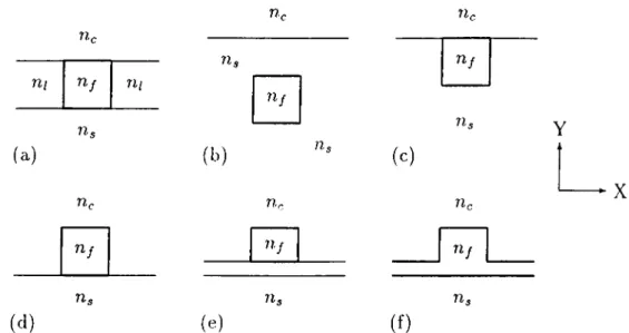
1.1 Cro.ss-sectional geometries of common channel waveguides : a) General channel waveguide, b) Bui'ied, c) Embedded, d) Raised, e) Ridge, f) Rib... 2
2.1 Example circuit illustrating the process of segmentation. (Path numbers are labeled at the inputs. Arrowheads indicate the o u tp u ts .)... 7 2.2 The signal and crosstalk levels at point B are approximated by
those at point D. 8
.'1.1 In segmentation algorithm, the fringing effect from the second guide to the first one is neglected... 12 .'5.2 Orthogonal bend implemented by total internal reflection. 14 .'I..'! An orthogonal intersection. Arrows represents direction of light. 14
4.1 First array-of-pointers ty]>e data structure for the circuit in Fig. 2.1... 18 4.2 Example circuit illustrating the creation of array-of-pointers
ty]>e data structures. (Path numbers are labeled at the inputs. .Arrowheads indicate the o u tp u ts .)... 18 4.8 Second array-of-|)ointers type data structure for the circuit in
Fig. 4.2. (N is the total number of rows in the rectilinear plane in which the circuit is em bedded.)... 18
4.4 -Segmentation algorithm for the interconnect portion AE after the neighbours are determined in both directions... 21
5.1 Example circuit having 15 paths and 320 segments... 24
6.1 a) General step index channel waveguide, b) Symmetric step index slab waveguide... 29 6.2 Separation of a channel waveguide into two symmetric step index
slab waveguides... 29
LIST OF TABLES
5.1 Output signal levels, output signal levels with respect to input signal, output crosstalk levels, and output crosstalk levels with respect to input signal for the example circuit with a grid spacing of 6 microns... 24 5.2 Output .signal levels, output signal levels with respect to input
signal, output crosstalk levels, and output crosstalk levels with respect to input signal for the example circuit with a grid spacing of 9 microns... 25 5..'3 Output signal levels, output signal levels with respect to input
signal, output crosstalk levels, and output cro.sstalk levels with respect to input signal for the example circuit containing 13 paths with a grid spacing of 6 microns... 26
Chapter 1
INTRODUCTION
It has been widely argued that the use of optical interconnections may provide several benefits over electrical interconnections in many situations [1, 2, 3, 4], [5, 6, 7]. In fully electrical systems, overall system speed tends to be lim ited by interconnect delays, and a relatively large portion of system power may be dissipated in the interconnections. Problems such as electromigra tion and electromagnetic interference contribute to the attractiveness of optical interconnections [1]. Among widely quoted advantages of optical interconnec tions are freedom from capacitive loading, freedom from planar or quasi-planar constraints, reprogramming or reconfigurability by means of a dynamic opti cal component, cind even the ])ossibility of direct injection of optical signals into electronic logic devices [1]. Some particular examples of practical im plementations are a multifiber bus for module-to-module connections, master card for backplane, waveguide arrays for multichip modules, and a chip level clock distribution demonstrator for chip level optical interconnections [8]. In a multifiber bus, several electronic circuit boards are connected by an array of optical star couplers via ribbon fibers. A mastercard uses total internal reflection in a glass slab, which is provided with holograms performing beam directing splitting and focusing functions, to guide collimated beams, from a source located on one daughterboard, to several receivers located on the other daughterboards. It is olivious that electrical crosstalk between j)arallel tracks becomes problematic as frequency increases. The crosstalk can be reduced to acceptable levels by using a waveguide array demonstrator with a waveguide separation of 10 /¿m and a length of a few tens of centimeters [8]. Comparisons of performance characteristics—such ¿is speed, bandwidth, power consumption.
(a) (d ) Hr rii n j --- ns Til 7lf n. Uf n.
(b)
(e) Uc nj 71, ( c ) (f) 7 l r Hf 71, Tlr nj 71, YX
Figure 1.1: (Jro.ss-sectional geometries of common channel waveguides : a) General channel waveguide, b) Buried, c) Embedded, d) Raised, e) Ridge, f) Rib.
footprint area—of electrical and optical or optoelectronic systems have been published [9, 10, 11, 12, 13].
Single mode channel waveguides can be made the basis of an integrated optics approach to providing optical interconnections. Several types of channel waveguides are shown in Fig. 1.1 [14, page 59]. Materials such as silicon nitride [15] or various polymers [16, 17] can be u.sed to realize the passive waveguides. Waveguide interconnects between chips on a multichip module, between in dividual chips or multichip modules on a printed circuit board, and between boards attached to a backplane have been studied before [18].
There are some certain differences between electrical and optical inter connections. In electrical integrated circuits, electrical interconnections have resistance which is inversely proportional to the width of the interconnects. However, in optical integrated circuits, loss is characterized by an attenuation coefficient instead. The minimum width of the optical channel waveguides is determined by the diffraction effects. Moreover, 90*^ bends are allowed for electrical interconnects l)ut they have also resistance problems. Especially, for the interconnects carrying a lot of current, these problems are more serious. Similarly, 90*^ bends can be used for optical interconnects and they are allowed in this study of analysis (see S(‘c. 3.4). Their loss mechanism is different from that in an electrical 90^ bend. Such considerations show the necessity for a (lifferent method of analysis for optical integrated circuits.
Quite popular simulation tools for optoelectronic circuits are already devel oped, but these are based on beam propagation method (BPM) [19, 20]. These software are quite accurate for simulation of optical features of optoelectronic devices such as X and Y junctions, polarization beam splitters, integrated receiver-guide circuits and integrated lasers. However, they are not designed, nor efficient for complex integrated optical circuits containing many paths and segments.
Despite such and similar efforts, no general approach towards the analysis and design of complex integrated optical circuits of arbitrary circuit diagram has been studied. Systems for analyzing and simulating electrical integrated circuits are many and well developed, as well as computer aided design systems for VLSI systems. An abstraction of design considerations has led to so-called design rules, such as the one stating that two parallel metal lines must be separated by a distance of at least 3A, where A corresponds to the smallest feature size of that technology [21, page 48].
The purpose of this study is to develop computer aided analysis and design systems, together with similar abstractions as mentioned above. These, it is hoped, will make the realization of complex optical circuits possible [22]. In this thesis, only the analysis and simulation are considered while mentioning how this analysis system can I)e made the basis of a design system. More concretely, a system calculating the loss and crosstalk for passive, single-mode, fairly complex waveguide circuits is reported.
In the system developed, the user enters the topology of the circuit to be analyzed using a cursor driven interface, and supplies the initial signal cind crosstalk levels at the inputs. The characteristic parameters of the waveg uides, such as their j^ropagation, attenuation, and coupling constants iire also specified. (An auxiliary program calculating these parameters in terms of the geometry and refractive indices of the materials for step index channel waveg uides is akso developed (see .Sec. 6.1). This approach can be generalized to waveguides of arbitrary cross-sectional profiles (Sec. 6.2).) When the program is executed, it determines the signal and crosstalk levels at any point in the cir cuit. Since the algorithm is very fast, adjustments can be made to improve the signal and crosstalk levels and the calculations are repeated several times until satisfactory differences in output signal and crosstalk levels are achieved in all interconnects. Thus, it is a short step from this analysis/siinulation system, to the realization of a design system.
In Clip. 2, the problem is stated by giving the inputs and the outputs, and the method is described by explaining shortly the algorithms which simplify the problem and by indicating creation of the equations leading to the solu tion. In Clip. .‘1, mathematical expressions for signal and crosstalk calculations at five different circuit structures, namely basic circuit features, are given. The fast algorithms developed, especially segmentation algorithm, are explained further in Clip. 4. Moreover, computer implementation of these algorithms are described in the same chapter by giving data structures, text files and a matrix equation created in the program. A circuit with 15 paths, and .320 segments after the segmentation algorithm, has been analyzed as an example by using the developed computer tool and the results are indicated in Clip. 5. In Clip. 6, two methods are summarized to calculate coupling coefficient be tween waveguides and power percentage propagating in the core region: In the first one, all the interconnects used in the circuit are assumed to be step-index channel waveguides (Sec. 6.1), and the waveguides are assumed to have arbi trary geometry and arbitrary index profile in the other one (Sec. 6.2). The use of this method, and thus that of the computer tool, and further possible improvements are discussed in Clip. 7.
Chapter 2
PROBLEM DESCRIPTION
AND APPROACH
Single-layer, planar integrated optical circuits of arbitrary topology and com plexity (with some restrictions), constructed of single-mode waveguides are analyzed in this thesis. Given the input signal and crosstalk levels, the output signal and crosstalk levels are determined. It is assumed that the circuits to be analyzed are rectilinear, so that the interconnects Ccin be mapped on a Carte sian grid. It is also assumed that the interconnections are one-to-one, fan-out and fan-in is not allowed. (Thus circuits in which such features exist or are desirable cannot be analyzed with the system. Allowing such interconnections greatly increases the difficulty of aiuilysis and simulation, so that removal of this restriction must be postponed for future research.)
It is assumed that all of the waveguides are of the same width, geometry and refractive index profile. The input is most likely a light source, and the output is most likely a light detector, both of which are probably situated on, or attached to, electronic integrated circuit chips. No assumption is made regarding the nature of these transducers, any imperfect coupling into or out of the optical circuit is lumped into efficiency factors Vontput· It
assumed that the light which cannot be coupled into its intended destination is |)roperly shielded, alisorbed, or diverted so that it does not leak into the circuit in an uncontrollable way.
affected in different ways by different circuit structures encountered, such as in tersections, bends, and parallel neighbours. In calculating the effects of these interactions between an interconnect path and its neighbours, only nearest neighbour waveguides are taken into consideration. This is most often ap propriate because the amount of coupling between two waveguides decreases exponentially with the separation between them (see Eq. 6.3 and Eq. 6.17 in Clip. 6). This does not mean however that farther neighbour effects are totally disregarded, the effect of a second nearest neighbour is accounted for indirectly (since an undesired signal component coupled from the second nearest to the nearest neighbour, will have an effect on the total signal coupled into the waveguide under consideration, via the coupling from the nearest neighbour [23]). Although this process is not exact, taking into account the coupling between each and every pair of circuit segments does not present itself as a formidable alternative, both from an analytical as well as from a computa tional perspective.
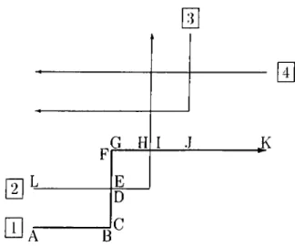
To calculate the coupling from neighbouring guides as going along a par ticular interconnection, the waveguide is mentally divided into what is called segments^ these are portions of an interconnection in which the circuit structure around that waveguide is unchanging. Segmentation will be further discussed in Sec. 4.1. However, the simple circuit shown in Fig. 2.1 can help under standing the main idea. Each letter in the figure indicates a point where the interconnect is broken into segments, thus segments can be represented by let ter pairs, such as CD. Some segments have a length, such as CD, .JK. Others do not, such as BC, DE. The signal and crosstalk levels associated with a .seg ment are those at the ending point of it, which is determined by the direction of propagation, thus the signal level of segment CD is the signal level at point D, .S£), and the crosstalk level of the same segment is the crosstalk level at the same point, /?.£). .Superposition can be used for field amplitudes. Therefore, instead of re])resenting signal and crosstalk levels by power intensities, it is preferred to use field amplitudes which are additive and are related to power intensities. Crosstalk is defined as the amount of signal coupled from neigh bouring waveguides, therefore it is deterministic. In the analysis, crosstalk can be considered as any signal disturbing the actual signal level. Therefore, the difference between signal and crosstalk levels at a point is the worst actual signal level that can be obtained at this point. Crosstalk in this analysis has two components; one is uncorrelated with the actual signal, and the other is correlated. (This will be explained further in this chapter.) The signal and
□ a B
0
G H E0
I J J<Figure 2.1: Exciinple circuit illustrating the process of segmentation. (Path numbers are labeled at the inputs. Arrowheads indicate the outputs.)
crosstalk at a segment depend on those at the previous segment and those at the segments of the nearest neighbouring waveguides. For example, the signal and crosstalk levels at point B in Fig. 2.1 depend on the signal and crosstalk levels at points A and L. Each path in the circuit is segmented individually, i.e. the segmentation is path dependent.
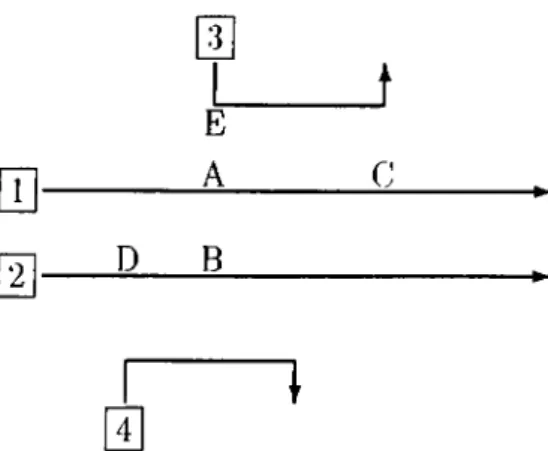
Because of the pcith-dependent nature of the segmentation algorithm de scribed above, one can face with the following problem: In Fig. 2.2, the signal and crosstalk levels at point C depend on those at points A, B and E. How ever, path 2 is not segmented at ])oint B thus, no signal or crosstalk element is associated to this point. In such a case, the signal and crosstalk values at B are approximated by those at D which are the values belonging to the previous segment. (Notice that the direction of propagation in path 2 is from left of the figure to the right.)
During segmentatioiu all the waveguides connecting the input and the out put of a path is traced. While going along a waveguide, the structure around is searched in the vertical direction to the waveguide to find the nearest paral lel waveguides on both sides. Any change in the structure of the neighbouring guides indicates that the present segment is ended ciiid a new segment should be created afterwards. Hence, in a single segment, the structure of neighbouring waveguides, i.e. closest parallel guides, does not change.
Segments are created with the pur])ose of isolating circuit features which are easily analyzed. As illustrated by the example, any circuit can be broken
m [ H -s
L
E ______ ^ D B C0
Figure 2.2: The signal and crosstalk levels at point B are approximated by those at point D.
down into five circuit features, i.e. basic elements of the circuit. Namely;
1. Stretch of waveguide with no neighbours
2. Stretch of waveguide with a neighbour on one side 3. Stretch of waveguide with neighbours on both sides 4. Orthogonal bend of a waveguide
5. Orthogonal intersection of two waveguides
For each interconnect, one should start with given signal and crosstalk levels at the input. Since the effect of each of the above circuit features are known, the loss in signal power and accumulation of undesired crosstalk, at the output can be calculated. Two field aiiiplitudes are used, one denoting signal level and one denoting crosstalk. (Ch’osstalk is defined so as to include all undesired coupling into the guide. If a detector is tied to the output, the thermal and shot noises associated with it must l)e added to the crosstalk level calculated at the output.)
It has been mentioned that cro.sstalk in the analysis has two components. If the correlated component of crosstalk is zero at a point, then the signal level in the analysis will be the actual signal level at this point. However, if the uncorrelated coinj^onent is zero, then the correlatetl component may be out of pha.se with the signal and this creates the maximum error in the signal calculation. Since it cannot be expected that there will be a predetermined or fixed ])hase relationship between the various light sources, it is assumed that
the phase relationships between the interacting signals are such as to result in the greatest increase in crosstalk, and greatest decrease in signal levels. This type of worst-case analysis is necessary, as the phases of the light sources may drift over time. As a result of this, if a desired difference between output signal and crosstalk levels is obtained for a path in the analysis, it means that one can actually get at least this value as the output signal in real life.
If the crosstalk and signal levels of all neighbouring interconnects were known to start with, one could calculate the signal and crosstalk levels at the output of a particular interconnect by working one’s way along each segment, from the light source to the detector (i.e. from point A to point K in Fig. 2.1). However, to begin with, the signal and crosstalk levels at any interconnect are not known. Thus, a system of equations relating all of the signal and crosstalk levels must be created and solved to obtain the desired output signal and crosstalk levels:
x = T x + l, (2.1)
where x is the vector whose elements are the signal and crosstalk levels for all the segments, T is the matrix relating the signal and crosstalk at any segment to those at previous segments and neighbours as explained in the next chapter, and 1 is the vector of input sources.
Chapter 3
SIGNAL AND CROSSTALK
LEVEL CALCULATIONS FOR
BASIC CIRCUIT FEATURES
For each interconnection path, starting from the source up to the detector, each segment can be modeled as one of the five elementary features mentioned in Clip. 2. The signal and crosstalk calculations for these live circuit features ¿ire described below.
3.1
str e tc h o f a Single W aveguide
First a certain length of a single waveguide in isolation can be considered. In analyzing a circuit, waveguides will be treated as such if their nearest neigh bours are sufficiently far away. By looking at Eq. 6.3 and Eq. 6.17 in Clip. 6, it can be said that coujiling between waveguides decreases exponentially with the separation between them. Therefore, if the separation between the waveguides is sufficient, the crosstalk between them can be ignored, i.e. the structure can be considered as a stretch of a single waveguide. The attenuation is assumed to be uniform along a waveguide“. Both signal and crosstalk components are attenuated liy a factor of where a is the attenuation coefficient and i is the length of this segment of the guide. For example, if .s and n are the signal and crosstalk levels, respective'ly, at the beginning of a single waveguide, the
= (3.1) signal and crosstalk levels at the end of the segment can be calculated by
n = ne (3.2)
The followings can be given as examples to the attenuation coefficient for TirLiNbOa: The loss is IdB /cm at A = 0.633/im, 0.!bdB/an at A = 1.15/im, and 0.2dBfcm at A = 1.52/im [24, page 224].
3.2
S tretch o f Tw o P arallel W aveguides
The following structure can be considered: on one side of the waveguide in consideration there is a parallel running waveguide, but on the other side the closest waveguide is far enough for its effect to be ignored.
In such a structure, if .S| and n\ are the signal and crosstalk levels of the first guide at the input side of the segment, and .s-2 and 712 are those of the second
guide, i is the huigth of parallel run along this segment, a is the attenuation coefficient along a waveguide, and k, is the coupling coefficient between the waveguides; then the signal and crosstalk levels of the first guide at the output are given by the following ecjuations [25, page 626]:
.s; = .si|cos(A>:^)|e·^^' , (3.3) n\ = [r^l cos(Ax:f)| + (S2 + n2)| sin(/c/^)|] -Ct( (3.4) Eq. 3.3 and Eq. 3.4 mean that in a parallel waveguide coupler, initial signal and crosstalk levels of the first guide are varied by a cosine term because of the effect of the neighbouring guide. Moreover, an additional term is added to the crosstalk expression. Its worst case amplitude is the maximum field available in the second guide times a sine term coming from the coupler characteristics. A worst [)hase relation between the lights propagating in l)oth guides is assumed therefore both the crosstalk terms are absolutely added. Finally, signal and crosstalk levels at the first guide are both exponentially attenuated by means of the attenuation constant, a.
If the directions of light ])ropagation in the waveguides of a coupler are opposit(', then the signal and crosstalk levels at the output of the first guide can be calculated as follows:
.s', = ,s, |cos(kO |c II
m
1
i
í
í
I
Figure 3.1: In segmentation algorithm, the fringing effect from the second guide to the first one is neglected.
n\ = ri\I cos(icf?)|e -Oti (3.6)
An approximation inherent in this method of analysis should be mentioned: As illustrated in Fig. 3.1, light propagating inside guide 1 interacts with light propagating in both the horizontal and the vertical portions of guide 2 because the evanescent tails of these fields overlap. However, the overlapping tails propagate in the opposite directions. Therefore, due to very similar reasons as in Marcatili’s “field of shadows” method explained in Sec. 6.1, the coupling from this interaction is very small. The effect of interaction with the vertical portion is somewhat analogous to the fringing effect in a parallel plate capacitor. As long as the distance of parallel interaction is long, the fringe effect can be neglected with small error. (If the distance of parallel interaction is small, this would mean that the overall coupling over this segment of the interconnect is small compared to other segments, so that again the error is small.) However, if one would like to consider the coupling from this interaction, a correction term similar to that used in accounting for the fringing effect in a parallel plate capacitor can be used.
3.3
s tr e tc h o f T h ree P arallel W aveguid es
Generally, a straight running waveguide, unobstructed by bends or intersec tions, will have neighbouring waveguides on both sides (unless it is at the edge of the circuit).
In a three i)arallel waveguide structure, if .sj, .s.-j and 7ii, are the signal and crosstalk levels of the outer guides at the input respectively, s-¿ and n-2 are
those of the center guide, Í is the length of the waveguides, and if a is the attenuation coefficient along a waveguide, the signal and crosstalk levels of the center guide at the output can l)e given by the following expressions [26, pages
136-137], [27]:
n-2 = П ‘2| COs(ac£ ) | + + П] ) —— I sin(AC^)| + (.S3 + ^ з ) “ ~ | ^5111(аС^)|
hb fx,
s'2 = .S2I cos(/c^)e (3.7)
(3.8) where k = yK^2+ ^ ^ ) ^¡j· coupling coefficient between waveguide i and
waveguide;, ( i,j) = {(1,2), (2,3)}.
It should be noted that the crosstalk from waveguides outside the first and third guides is ignored because of the same reasoning explained in Clip. 2.
If the first and the second guides are in the same direction and the third one is in the opposite direction in a three-guide-coupler, then the signal and crosstalk level calculations at the output of the second guide are given by
^2 = cos(«:^)]e'
n.y = U‘2 I COs(/C^) I + + T'il ) —— I sin(AC>^) |
(3.9) (3.10) If the direction of the second guide would be different from the other two, then the crosstalk term coupled from the first guide to the second one in Eq. 3.10 would not be present.
3.4
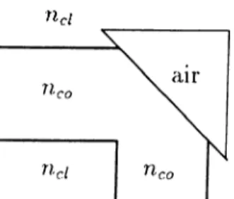
O rthogonal B en d
In most cases, each interconnection will suffer from at least one 90° bend. Smooth curved bends take up too much space, requiring as much as a 1 cm radius in weakly guiding waveguides in Ti:LiNb()3. Obviously this limits the packing density considerably. For this reason, for right or left turns, total internal reflection mirrors, as in Fig. 3.2, are assumed. Due to the large index difference Iietween core and air at the corner, the reflection coefficient is very close to unity ([24, page 229]). Such a bend can be characterized by an efficiency factor r/i,, which accounts for the power loss as a result of the bend. (The loss can be mostly attributed to the ¡oower traveling outside the core, which cannot l)e i)erfectly reflected. This suggests an approximate way of calculating the efficiency factor. See Sec. 6.1 and Sec. 6.2.) At an orthogonal bend, there is of course a reflected signal. Its effect is included in the power efficiency factor, 7/;,, as a loss. However, in the analy.sis, the reflected signal is not coupled into any signal or crosstalk variable because it propagates through the input side of
Figure 3.2: Orthogonal bend implemented by total internal reflection.
2’
f
-1’
Figure 3.3: An orthogonal intersection. Arrows represents direction of light. the path, i.e. its effect cannot be seen at the output, and any further coupling is ignored as a higher order effect (just as ignoring coupling to non-nearest neighbours). Therefore, if the signal and crosstalk levels before an orthogonal bend are ,Si and n-i, respectively, then those after the bend, .sj and nj, can be related as
= \/Vb^h ■
(3.11) (3.13)
3.5
O rthogonal In tersectio n
Unless multi-layer optical circuits can be realized, intersection of waveguides will be unavoidable. The loss and crosstalk is very angle sensitive and the loss is minimum for normal intersection, which is the only kind possible for rectilinear circuits anyway. As with bends, the loss and crosstalk can be characterized by efficiency factors ?/, and r/c- The first one corresponds to total ¡lower coupled from direction 1 to direction 1’ in Fig. 3.3 considering the calculation of light power ])ropagating in the horizontal direction from left to right. The other factor represents the power coupled from direction 2 to direction 1’ in Fig. 3.3.
Therefore, the signal and crosstalk levels in the horizontal waveguide in Fig. 3.3 can be calculated by using the following equations;
•s'l - a/^-5i , +ri2) .
(3.13) (3.14)
C h a p ter 4
METHOD OF ANALYSIS
AND SIMULATION
The algorithm and computer im])lementatioii of the analysis described in Clip. 3 will be given in this chapter. Although the process of segmentation and calculation of crosstalk and coupling are easy to grasp intuitively, develop ing the appropriate data structures and procedures that result in a fast analysis system is not straightforward.
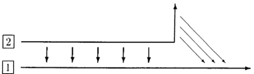
In the implementation, the user enters the circuit to be analyzed by using a cursor driven interface. Interconnects must follow the Cartesian grid, whose spacing in microns, i.e. grid spacing, is specified by the user. (Minimum dis tance between two waveguides should not be smaller than twice the width of a waveguide.) The resolution of the circuit is determined by the pixel length of the computer screen. Therefore, the grid spacing can be entered by giving the number of pixels that will be considered as one grid. While the circuit topology is being entered, three different data structures are created simul taneously. Tliey are all array-of-i)ointers type data structures and store the circuit topology in the following manner:
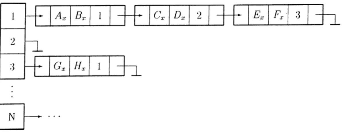
1. In the first one, each pointer in the array represents an interconnect path and each cell of the pointer c.orresi)onds to an orthogonal bend in this l^ath. A new cell is added to the pointer when a new ijend is entered to the i)ath by the user. Therefore, all the bends are stored in the correct order. For example, for the circuit shown in Fig. 2.1 the first pointer of
the array contains the information about the first path in the circuit (see Fig. 4.1). The first cell of the pointer maintains the coordinates of point A {Ax: abscissa of point A and Ay\ ordinate of the same point in Fig. 4.1) which is the input of the path. In the same manner, the second cell is for the coordinates of point B, third cell is for those of point F and finally the fourth one, the last cell, for point K which is the output. There are totally four cells in the pointer and they are in the correct order from the input to the output.
2. Each element of the second array corresponds to a horizontal line, i.e. row, in the Cartesian grid in which the circuit is embedded. Each cell of a pointer represents a horizontal interconnect portion between two consecutive bends of a path lying on the corresponding row. The cells of the pointers are sequenced with respect to the abscissa of the left starting point of the horizontal interconnect portion. The first pointer of the array represents the lowest horizontal line of the rectilinear Cartesian plane containing the circuit. In the circuit shown in Fig. 4.2, without loss of generality it can be assumed that the inputs of the first and third paths are located at the first horizontal line of the plane. Then the first pointer of the array represents all the horizontal interconnect portions lying on this line (see Fig. 4.3). The first cell contains the information about the first interconnect portion (AB) on this line, namely the abscissa of points A and B {Ax and Bx, respectively), and the path number which is 1. The second cell contains the abscissa of points C and D {Cx and Dx, respectively), and the path number which is 2, the third cell maintains the abscissa of i)oints E and F, and the path number which is 3. There are totally three cells in the j)ointer and they are in the correct order from left to right. There is no interconnect portion in the second row of the circuit shown in Fig. 4.2 therefore, the pointer corresponding to the .second element of the array is simply a nil pointer (.see Fig. 4.3). In the circuit, there is only one horizontal interconnect portion in the third row thus, the pointer belonging to the third element of the array has only one cell. The rest of the array is created in the same manner. In this structure, there is an empty element for each row in the circuit which does not contain any waveguide interconnect portion.
3. The third array is very similar to the second array but stores the vertical interconnect portions instead of horizontal ones.
Figure 4.1: First array-of-pointers type data structure for the circuit in Fig. 2.1.
Row 3 Row 2 Row 1
Figure 4.2; Example circuit illustrating the creation of array-ot-pointers type data structures. (Patlı numbers are labeled at the inputs. Arrowheads indicate the outputs.)
Figure 4.3: Second array-of-pointers type data structure for the circuit in Fig. 4.2. (N is the total number of rows in the rectilinear plane in which the circuit is embedded.)
After giving the circuit layout, other inputs to the analysis system should be specified. They are, namely, attenuation coefficient along a waveguide whose unit should be m “ *, actual grid length in /m i’s to be able to determine the actual sizes of the circuit, signal and crosstalk (normalized) field intensity levels at the input laser sources (unitless) and wavelength of light from the laser .sources in /im ’s.
If the coupling etc. parameters are not specified, they can be calculated by using one of the methods summarized in Clip. 6. The first method assumes step index channel waveguides as optical interconnects and is available in the computer tool developed. It needs cross-sectional geometry and the index profile of the step index channel waveguides as inputs. If the geometry or index profile of the waveguides used as interconnects are different, some work should be done outside the environment of the computer program by using the method described in Sec. 6.2. However, the way of these calculations does not affect the present analysis system.
The computer tool developed for the implementation of the analysis is writ ten by using Turbo Pascal, version 6.0, and Turbo C Programming Languages for personal computers. The latter is used only for the solution of Eq. 2.1.
4.1
S eg m en ta tio n A lg o rith m
The segmentation of each interconnect path is the most important part of the program. A segment is defined as a part of a path which forms one of the basic circuit features described in Clip. 3 (see also Fig. 2.1). The signal and crosstalk levels at any segment of a path depend on those at the ])revious segment of the same path and those at neighbouring paths.
A text file is created to store the segments from segmentation algorithm. Segmentation starts from the source of the first path and continues towards the detector of this path. When segmentation in the first path is finished, it continues on the second path, third path, etc. In the text file, all the data about a segment is stored in a row. These data contain the path number, direction, and coordinates of the .segment, and distances to the neighbours (if exist), and directions of the neighbours.
The .segmentation starts by writing the source and bend points ot a path,
which are available in the first array of pointers, shown in Fig. 4.1. They are listed into the text file in the correct order, which is the order in the first array-of-pointers type data structure. Signal and crosstalk variables will be associated to the end of each segment. Therefore, detectors are not segments because the segment ending with a detector has the signal and crosstalk values of the detector.
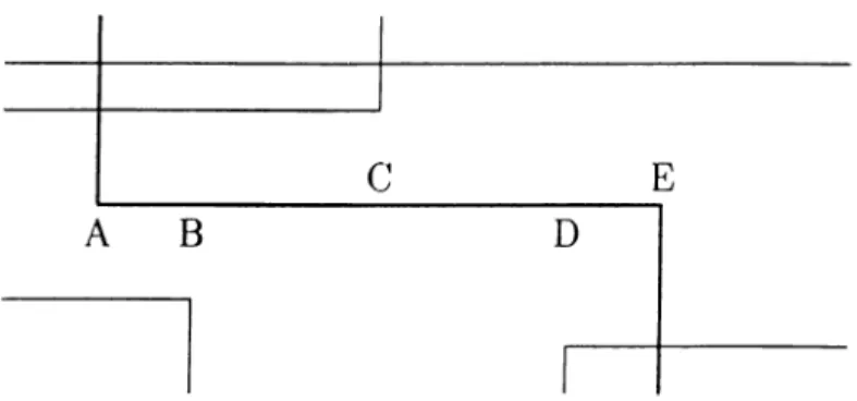
After writing the source and bends of a path into the text file, each straight waveguide between two consecutive bends, i.e. interconnect portion, is seg mented by using the third array-of-pointers type data structure if the inter connect portion is horizontal. The elements of this array between the abscissa of the starting and ending points of the interconnect portion are searched for vertical interconnect ¡portions intersecting with the analyzed horizontal inter connect portion. The intersection points are written into the text file as new segments between the starting and ending points of the horizontal interconnect portion.
After an interconnect portion is segmented, each straight waveguide be tween two consecutive intersections or between an intersection and a bend, i.e. an interconnect unit, is segmented by using the following algorithm: Assume that the interconnect unit is horizontal. In the second array of pointers, shown in Fig. 4.3, the row just above the one containing this interconnect unit, i.e. the following element in the array, is searched for an interconnect portion whose x- coordinates may overlap with those of the analyzed interconnect unit. If there exists any overlapping part, the overlapping x-coordinates and the distance to the analyzed interconnect unit are stored in a single cell of a pointer type data structure and the x-coordinates covered already are stored in another pointer. The same procedure is continued for the following rows in the array. When a new overlapping part is realized, its x-coordinates are compared by the pointer containing the covered portions of the interconnect unit. If any part ot the overlapping interconnect portion has not been covered yet, then this portion is added to the pointer of covered portions as a new cell in the correct se- c|uence which is determined by the x-coordinates. Moreover, the same part is stored as another new cell in the other pointer by including the distance to the analyzed interconnect unit, again in the correct order. When all the interconnect portions are covered by neighbours in the up direction, the same procedure is ajiplietl for the lower neighbours and another pointer is created for them. Next, by considering both pointers together, one for upper and the other for the lower neighbours, the analyzed interconnect portion is segmented
Figure 4.4: Segmentation algorithm for the interconnect portion AE after the neighbours are determined in both directions.
in the horizontal direction. For example, interconnect portion AE in Fig. 4.4 is visually segmented by using the pre-determined neighbours in the up and down direction. The segments AB, BC, CD and DE are the resultant segments after the segmentation algorithm. These segments are written in the correct order between the bends A and E in the text file containing the segments. If the analyzed interconnect unit is vertical, the same procedure is applied for left and right parallel neighbours by using the third array-of-pointers. After this algorithm is applied to the whole circuit, the text file will contain all the segments in the correct order starting from the input of the first path to the output of the last one.
It can be easily seen from the algorithm that segmentation is path depen dent. For example, in the circuit shown in Fig. 2.1 the horizontal interconnect unit of the third path between the intersection with the second path and the out])ut is divided into two different segments, which is not indicated in the fig ure (only the first path is segmented), because of the presence of the segment GH of the first path. However, the horizontal interconnect unit of the fourth path between the intersection with the second path and the output corresponds to a single segment l^ecause segment GH is not a neighbour of this interconnect unit.
4.2
C reation o f th e M a trix E q u ation
After all the interconnect paths are segmented, x and 1 vectors, and T matrix in Eq. 2.1 should l)e created. The elements of vector x are signal and crosstalk values of the segments stored in a text file in the correct order as ex])!aimxl in
Sec. 4.1. This vector is the unknown vector to be solved in Eq. 2.1. Vector 1 contains the signal and crosstalk values of input sources and they are stored in another text file. Matrix T , which is a square matrix, maintains the coefficients relating the signal or crosstalk values of a segment to those of the previous segments and of neighbours. They are stored in a two dimensional array with a size twice the total segment number because each segment has one signal and one crosstalk value. All the data necessary to calculate the coefficients in the transfer matrix are written in the text file containing the information about the segments (see Sec. 4.1). The calculation methods which are given in Chp. 3 are created as procedures in the computer tool developed and are used at each time during the creation of the transfer matrix.
4.3
S olu tion o f th e M a trix E q u ation
In the analysis, the major goal is to find the signal and crosstalk values ev erywhere in the circuit. Therefore, Eq. 2.1 should be solved as explained in Chp. 2. To succeed this, a program for solving sparse matrices is used. It is written by using Turbo C Programming Language and solves the x vector in the equation
x = ( I - T ) - ‘I (4.1)
where I is the identity matrix. The efficiency of the sparse matrix solver pro gram is inversely related to the maximum number of elements in a row of the matrix (I — T). In the analysis, this number is 6 whatever the segment number thus, the sparse matrix solver gives the results very accurately. Moreover, it can be said that this solver is also very fast. After the program is executed, the signal and crosstalk values at any segment can be obtained from the text file containing the x vector.
The details about the si>ar.se matrix solver program are not given here because they are out of the thesis context.
Chapter 5
EXAMPLES AND RESULTS
For purpose of illustration, the results for the circuit shown in Fig. 5.1 with 15 interconnect paths are presented. This circuit, which lays on a square with an area of 96 /mi x 96 /.im, turns out to have 320 segments.
All the channel waveguides used as interconnects in the examples below have a width of 3 /¿m, a thickness of 1 /mi, refraction indices of 3.5 in the core region, 3.45 in the lateral direction, 3.4 in the cladding region and an attenua tion constant of 100 m“ F The wavelength of light is assumed to be 1 /mi. The minimum grid spacing is taken as twice the width of the waveguides which is
6 fim. At this grid spacing, coupling coefficient between two waveguides, k, is
12.365 m ~', efficiency factor at an orthogonal bend, ?/(,, is 0.849 which is per centage of power jiropagating in the core region of a waveguide in the analysis (see Clip. 6). Similarly, the iirsertion loss at an orthogonal intersection, 7/j·, is calculated as 0.849 and the crosstalk, is assumed to be so small to be equal to zero.
The signal and crosstalk levels at the inputs are taken to be 1 and 0, re spectively (in arbitrary units). The corresponding signal and crosstalk levels at the outputs are given in table 5.1. (The effects of any unwanted stochastic signal (noise), and thermal and shot noises of detectors at the outputs can be incorporated by a straigfitforward extension of the present example.)
The lowest difference between output signal and crosstalk levels occurred for path 12. Notice that this path is one of the longest paths and has the most bends.
Figure 5.1; Example circuit having 15 paths and 320 segments.
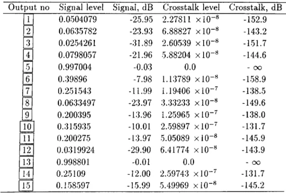
Output no Signal level Signal, dB Cro.sstalk level Crosstalk, dB 0.0508331 0.0639992 0.0256252 0.0803823 0.998501 0.399918 0.252677 0.0638841 0.201178 -25.88 -23.88 -31.83 -21.90 -0.01 -7.96 -11.95 -23.89 -13.93 2.97129 xl0~® 8.96528 xlO"® 3.38377 xlO-^ 7.65181 xlO-^ 0.0 1.47969 xlO-^ 1..5.5254 x l 0 - ‘‘ 4.34186 xlO-'^ 1.6.3574 x l 0 - ‘‘ -90..54 -80.95 -89.41 -82.32 - oo -96.60 -76.18 -87.25 -75.73 10 0.3174.55 -9.97 3.37644 x lO -“ -69.43 11 0.201118 -13.93 6.57391 xlO-^ -83.64 12 0.0322236 -29.84 8..34746 xlO-'^ -81..57 2 1 0.9994 -0.01 0.0 - oo 0.25245 -11.96 3.37468 xlO-'· -69.44 15 0.159647 -15.94 7.1.5206 xlO-·^ -82.91
Table 5.1: Outj)ut signal levels, output signal levels with respect to input signal, output crosstalk levels, and output crosstalk levels with respect to input signal for the example circuit with a grid spacing of 6 microns.
Output no Signal level Signal, clB Crosstalk level Crosstalk, dB 1 2 3 4 5 6 7 £ £
I£
H
13 ¿4 15 0.0504079 0.06.35782 0.02.54261 0.0798057 0.997004 0.39896 0.251,543 0.063.3497 0.200395 0.315935 0.200275 0.0319924 0.998801 0.25109 0.1.58,597 -25.95 -23.93 -31.89 -21.96 -0.03 -7.98 -11.99 -23.97 -13.96 -10.01 -13.97 -29.90 -0.01 -12.00 -15.99 2.27811 xlO“* 6.88827 xlO-*^ 2.60.539 xlO-*^ 5.88204 xlO"^ 0.0 1.13789 xlO-*^ 1.19406 xlO"^ 3.33233 xlO-® 1.2.5965 xlO-^ 2.. 59897 x lO -' 5.0. 5089 xlO-« 6.41774 xlO"*^ 0.0 2.. 59743 x lO -' 5.49969 xlO-® -152.9 -14.3.2 -151.7 -144.6 - oo -1,58.9 -138.5 -149.6 -1.38.0 -131.7 -145.9 -143.9 - oo -131.7 -145.2Table 5.2: Output signal levels, output signal levels with respect to input signal, output crosstalk levels, and output crosstalk levels with respect to input signal for the example circuit with a grid spacing of 9 microns.
For most of the applications, some of the differences between output signal and crosstalk levels in this example would not be considered sufficient so that alterations in the design will be needed. Therefore, the same circuit with the same circuit j)arameters and inputs is analyzed by only changing the grid spacing to 9 /tm. In this case, the coupling coefficient, «, becomes 0.0047732
The output signal and crosstalk levels are given in table ,5.2.
The ])ath with minimum ovitput signal and crosstalk difference is again path
12.
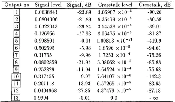
As another example, the circuit containing only the first 13 paths of the circuit shown in Fig. 5.1 is analyzed by using the same parameters and the inputs of the first example in which the grid spacing is 6 /mi. In this case, the circuit consists of 259 segments. The output signal and crosstalk levels are given in table 5.3.
In this example, the path with minimum output signal and crosstalk dif ference is path 2. In the first example, output 12 has the minimum difference. Notice that in the circuit, path 15 has a parallel run with path 12 and path
O utput no Signal level Signal, dB Crosstalk level Crosstalk, dB 10 13 0.0638841 0.0804306 0.0322043 0.126956 0.998501 0.502595 0.31755 0.0802859 0.252829 0.317455 0.201118 0.0404968 0.9994 -23.89 -21.89 -29.84 -17.93 -0.01 -5.98 -9.96 -21.91 -11.94 -9.97 -13.93 -27.85 -0.01 3.06907 xlO-^ 9.35479 xlO-^ 3.54538 xlO-^ 8.06475 xlO-^ 1.00813 xlO-'^^ 1.8596 xlO-" 1.7253 x lO -“» 5.08062 xlO-5 1.64524 xlO-^ 7.64107 xlO-« 6.57265 xlO"^ 4.37479 xlO-^ 0.0 -90.26 -80.58 -89.01 -81.87 -419.9 -94.61 -75.26 -85.88 -75.68 -142.3 -83.65 -87.18 - oo
Table 5.3: Output signal levels, output signal levels with respect to input signal, output crosstalk levels, and output crosstalk levels with respect to input signal for the example circuit containing 13 paths with a grid spacing of 6 microns. 14 has a parallel run with path 2. Both separations are the same, one grid, and the lengths are 5 and 8, respectively. As expected, the decrease in the output crosstalk level is larger for path 12 because the directions of paths 12
and 15 are the same but those of paths 2 and 14 are not. This means that the contribution from path 15 to the crosstalk term in path 12 is larger. The steepest increase in output signal and crosstalk differences is occurred in path 10. The main reason for this increase is the absence of path 14 (which has a long parallel run with path 10) in one of the examples.
For a test of .self-consistency of the analysis system, the circuit in the first example (15 paths, 320 segments, grid length of 6 /rm) is analyzed by using two different methods. In the first method, all the signal and crosstalk levels at the inputs are assumed to be 1 and 0, respectively. At path 12, the output signal level with respect to input signal level is -29.84 dB, the output crosstalk level with respect to input signal is -81.568913 dB. In the second method, input signal of only one path is 1 at a time. In this way, the output signal and crosstalk levels of the twelfth path are going to be analyzed. When the input of this path is executed, the signal level at the output of the path is the acttial signal level. This is again equal to -29.84 dB (compared to input signal). When input 1 is executed, the signal level at the output of path 12
is the crosstalk coupled from path 1 to path 12. In the same way, if all such crosstalk contributions from the other paths are added absolutely, this gives the actual crosstalk level at the output of path 12 which is equal to -81.568916 dB. It can be easily seen from this example that the signal levels at output 12
are equal in both methods and the difference in the crosstalk levels is in the order of 10~^. This shows the self-consistency of the superposition assumption used in the analysis.
In the computer program, it takes totally about .3.5 seconds to solve the circuit in Fig. 5.1 by using 80486 personal computers. The execution time reduces to about a second for smaller circuits with a number of segments below 100. The limitations of the computer tool mainly comes from dynamic memory limitations of personal computers. For example, for circuits having more than 350 segments, the computer program creates all the segments correctly however cannot solve the matrix equation. There is a sparse matrix solver available in the work-stations, which is actually another version of the sparse matrix solver used in the analysis. The input to this matrix solver can be given as well as the output can be obtained in the same way as the PC version of it. The speed of the program is comparable to the PC version when executed in the SPARC work-stations. There is no memory problem for this program; circuits having ten thousands of segments can be solved without any problem.
Chapter 6
CALCULATION OF
WAVEGUIDE CIRCUIT
PARAMETERS
It should be emphasized that the method of analysis and simulation discussed until now is independent of how the attenuation, propagation, and coupling parameters of the waveguides are calculated. These should be considered sim ply as inputs to the system. The exact profile or refractive index distribution are not relevant for the programs developed, their effect is summarized in the mentioned parameters. Such parameters may be numerically calculated, or even experimentally determined. In this chapter, an analytic approach for cal culation of these parameters for step index channel waveguides, and how the procedure can be extended to waveguides of arbitrary profile will be described (28).
6.1
s t e p In d ex C h an n el W aveguid es
In a general step index channel waveguide, Fig. 6.1.a, the eigenvalue equations for the weakly-guiding (m,n)th mode [29, page 44] are given by
, _] 7'i I . -I 7s
k.j.w = tan ---1- tan -— f- rnir ,
ti/qr (6.1)
(a) t ---W ---► ri2 ns n , Tl4 « 2 (b) nd Hr Y X
Figure 6.1: a) General step index channel waveguide, b) Symmetric step index slab waveguide. ri3 ri2 rii n-2 \/«2 - « i/2 n.3 = + \/n j - ^ ^ 7 i j - n i / 2 \ A 5
-Figure 6.2: Separation of a channel waveguide into two symmetric step index slab waveguides.
kyt = tan * ^ + tan ‘ ^ + riTT ,
hy ky (6.2)
where = \fk'o7ii — fp, ko = 27t/A, A: wavelength of light propagat ing inside the waveguide, 7.1 = \Jk'o{7).'i — 7i\) — k'^, 75 = \Jkl{7i\ — n',) — kl^
72 = - n.^) - k:^ and 73 = yjkl{7i\ - - k'^.
For fundamental T Eqq mode, i.e. m =n=0, the ecfuations are solved numeri
cally for k^ and ky by using Newton-Raphson method. The coupling coefficient between two ])arallel waveguides, ([29, i>age 52]), can be calculated by
2^'^72e-'>^'' /^(lT -f2/72)(^-^+ 7l) where d is the separation between the waveguides.
(6.3)
For the calculation of the percentage of power propagating in the core re gion, one can use Marcatili’s “Fields of Shadows” method, ([14, pages 63- 65]), in which, the waveguide is separated into two symmetric slab waveg uides as shown in Fig. 6.2. The refractive index of the shaded regions is -f ii.3 — nf . This method is very accurate for well-guided case. When the indices of the shaded regions are deviated from + — tii , the error made in this method starts to increase.
For a symmetric step index slab waveguide, Fig. G.l.b, the following eigen value equation for the weakly-guiding fundamental mode, ([29, page 38]), is solved numerically for ft by using Newton-Raphson method:
— fP —■ 2 tan- 1
i
cl
W = U tan U (6.4)
where V = ko^^/ri^^ - rP,i , U = {yjkin'll - (P , W = {\J(P - k^n% and t is the thickness of the core region. The percentage of power propagating in the core region for TE modes can be calculated by ([30, page 243]
?; = 1
-R2(l -b W) ■ (6.5)
By multiplying the power percentages for the two slab waveguides, the per centage of power propagating in ni-region of the channel waveguide, which is equal to both rji, and rji (see Sec. 3.4 and Sec. 3.5, respectively), is calculated.
The Newton-Raphson method mentioned above should be used carefully because the eigenvalue equations are not well-behaved functions thus, the con vergence may become a problem. To overcome this problem, a suitable initial value should be selected. Moreover, this initial value should be in the single mode region because it is assumed that all the waveguide interconnects used in the analysis are single-mode waveguides.
6.2
A rb itrary W aveguid e G eo m etry and A r
b itrary P rofile
If arbitrary waveguide geometry and arbitrary index profile are given, “equiv alent optical waveguide” method given in [31] can be used to calculate the coupling coefficient between two waveguides and the percentage of power prop agating in the core region. In this method, general moment of a waveguide is defined by the following equation (observe that the refractive index of the cladding is assumed to be uniform in the equation);
M (6.6)
For fundamental modes, two waveguides are equivalent if their zeroth and 30
second moments are equal:
^00 — ^^00 ·>
M2Q + = ^ 2 0 + Mq2 ·
If the first waveguide is circular, then one can get = 27r7V<‘^ , + mS = 2Tryvi') , (6.7) (6.8) (6.9) (6.10)
where the m-th moment of a circular waveguide, (guide i), is defined by roo
N i ; = (6.1 1)
-'0
If the first waveguide is a step index circular waveguide with radius a, then
= j i n l n l d
-(6.12)
(6.13) Hence for an arbitrary waveguide, the equivalent step index fiber can be deter mined by a = 2M¡S + Mo, C^) M (i)00 -- nil + (M<">^00 2,r(A/£' + Mi'']'·(•¿)l (6.14) (6.15)
After finding the equivalent step index fiber, the following eigenvalue equa tion for the fundamental H E\\ mode is solved numerically for U,
u ' l m =
M U ) I<o{W)
(6.16) where Jo fi'Hcl J\ Bessel functions of the first kind, Kq and K\ are Modified
Bessel functions of the second kind.
In weakly guiding case, cou])ling coefficient between two parallel waveguides is given by [30, i)age 392]
K = 7tA IP e ^ ^ - n'ii W daV '^K '^iW ) ’■
31
where d is the separation between the waveguides.
In a step fiber, for weakly guiding fundamental H E n mode, percentage of power propagating in the core region, ([30, page 257]), is given by
i/2
f/2 K H W) (6.18)
In the analysis, all the power propagating in the cladding is assumed to be lost at an orthogonal bend, i.e. the total power propagating after the bend is equal to the power propagating in the core before the bend, i.e. r/ = tjij. (See Sec. 3.4.) At the time being, the same assumption for the loss at an intersection have been made, i.e. j] = 7/,·. (See Sec. 3.5.)
Similarly, equivalent step-index channel waveguide (Fig. 6.1.a) of an arbi trary waveguide can be found by using the following equations:
77] =
where Mqq is the zeroth, and M20 and Mq2 are the second order moments of
the arbitrary guide; Ud is the refractive index in the uniform cladding.
After finding the eciuivalent step-index channel waveguide of an arbitrary guide, the coupling coefficient and ]>ower percentage propagating in the core region can be calculated by using the methods explained in Sec. 6.1.
K , + f(^).. 'W = V