Plasmonic gratings for enhanced near infrared sensitivity
of Silicon based Schottky photodetectors
Kazim Gurkan Polat1, Levent Erdal Aygun1, Ali Kemal Okyay1,2 1
Bilkent University, Department of Electrical and Electronics Engineering, Bilkent, TR-06800, Ankara, Turkey
2 UNAM-Institute of Materials Science and Nanotechnology, Bilkent University, TR-06800, Ankara, Turkey
*Tel:+90 (312) 290 1557, email: [email protected]
Schottky photodetectors have been intensively investigated due to their high speeds, low device capacitances, and sensitivity in telecommunication standard bands, in the 0.8µm to 1.5µm wavelength range. Due to extreme cost advantage of Silicon over compound semiconductors, and seamless integration with VLSI circuits, metal-Silicon Schottky photodetectors are attractive low cost alternatives to InGaAs technology1. However, efficiencies of Schottky type photodetectors are limited due to thin absorption region. Previous efforts such as resonant cavities increase the sensitivity using optical techniques, however their integration with VLSI circuits is difficult. Therefore, there is a need for increasing Schottky detector sensitivity, in a VLSI compatible fashion. To address this problem, we design plasmonic grating structures to increase light absorption at the metal-Silicon Schottky interface. There are earlier reports of plasmonic structures to increase Schottky photodetector sensitivity2,, with a renowned interest in the utilization of plasmonic effects to improve the absorption characteristics of metal-semiconductor interfaces3. In this work, we report the design, fabrication and characterization of Gold-Silicon Schottky photodetectors with enhanced absorption in the near infrared region.
Fig. 1: (a) MSM photodetector structure (b) Gold grating design on Si with parameters P: period, t: thickness, w: width and also polarization of incidence light
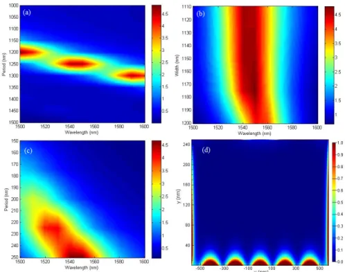
Silicon is infrared-blind (above λ=1100nm), however, Au-Si pair can absorb, although weakly, up to λ=1600nm. We design and optimize nanometallic gratings that provide local field enhancement in the vicinity of the metal-semiconductor interface for considerable absorption enhancement at 1550nm. We used finite-difference time-domain analysis to computationally calculate field profiles in our structure, using Lumerical FDTD Solutions. Fig. 1 illustrates the proposed nanometallic grating design. Electric field intensity at the interface is maximized for highest absorption assuming transverse-magnetic (TM) polarized illumination. Fig. 2 plots the field profile and effects of the parameters on the absorption enhancement.
Au-Si Schottky photodetectors are fabricated and metallic gratings are patterned using focused ion beam tool. Spectral characterization of the photodetectors exhibit improved sensitivity in the near infrared as shown in Fig. 3. We record 150mA/W responsivity at 1550nm illumination.
1
Luan, H.‐C., “Ge Photodetectors for Si Microphotonics”, PhD Thesis, Massachusetts Institute of Technology, February 2001, p. 21
2 Scales et.al IEEE JOURNAL OF QUANTUM ELECTRONICS VOL. 46, NO. 5, MAY 2010 3 Knight, et al. Science 332, 702 (2011);
733 ThI3 (Contributed Oral)
11:30 AM – 11:45 AM
Fig. 2: Electric field intensity is integrated over interface and normalized with respect to periodicity is given in (a-c) for arbitrary unit. (a) For constant thickness 250nm, width 1150nm. (b) For constant period 1250nm, thickness 250nm. (c) For constant thickness 250nm, width 1150nm. (d) Electric field intensity profile inside gold grating for metal width 1150nm, and thickness 250nm.
Fig. 3: (upper) SEM pictures of the fabricated Schottky photodetector with Si/Al2O3(2nm)/Ti(3nm)/Au(250nm), (bottom left)
responsivity of the device, (bottom right) Generated photocurrent dependence with respect to the polarization of light