FULL-DUPLEX MRI FOR ZERO TE
IMAGING
a thesis submitted to
the graduate school of engineering and science
of bilkent university
in partial fulfillment of the requirements for
the degree of
master of science
in
electrical and electronics engineering
By
Maryam Salim
May 2016
Full-duplex MRI for zero TE imaging By Maryam Salim
May 2016
We certify that we have read this thesis and that in our opinion it is fully adequate, in scope and in quality, as a thesis for the degree of Master of Science.
Ergin Atalar (Advisor)
Nevzat G¨uneri Gen¸cer
Ayhan Altınta¸s
Approved for the Graduate School of Engineering and Science:
Levent Onural
ABSTRACT
FULL-DUPLEX MRI FOR ZERO TE IMAGING
Maryam Salim
M.S. in Electrical and Electronics Engineering Advisor: Ergin Atalar
May 2016
In this thesis a new method for decoupling of RF transmit and receive coils in MRI is presented. A modified version of isolation concept used in the full-duplex radios in communication systems is applied to acquire MRI signal using concur-rent excitation and acquisition (CEA) method. Since in MRI transmit power is many orders of magnitude larger than receive signal, a weak coupling might dominate the MR signal during CEA in MRI. In our new method, a small copy of RF transmit signal is attenuated and delayed to generate the same coupling signal which is available in the receiver coil then it is subtracted from the receive signal in order to detect the MRI signal.
The proposed decoupling method is developed and implemented in two designs. First a semi-automatic controllable decoupling design which uses a programmable attenuator and coaxial cables for the purpose of time delay. After estimating the length of coaxial cables an optimization algorithm finds the amount of attenuation factor. Using this method we could achieve more than 75 dB decoupling.
Second design is a fully-automatic controllable decoupling design which con-tains four delay and attenuator lines. In this design four fixed phase shifters are used in order to generate the same phase delay between transmit and receive coils. A genetic optimization algorithm is used to find the amount of attenuation factors of each line. It is shown that this method provides more than 100 dB decoupling between transmit and receive coils which is good enough for detecting MRI signals during excitation from tissues with very short relaxation time.
This study shows feasibility of applying full duplex electronics which is used in telecommunications, to decouple transmit and receive coils for MRI with CEA, using a clinical MRI system. This device can automatically tune the cancellation circuit and it is a potential tool for recovering signal from tissues with extremely
iv
short T2 in clinical MR systems.
¨
OZET
SIFIR EKO-ZAMANI G ¨
OR ¨
UNT ¨
ULEME IC
¸ IN TAM
C
¸ ˙IFT Y ¨
ONL ¨
U MRG KULLANIMI
Maryam Salim
Elektrik ve Elektronik M¨uhendisli˘gi, Y¨uksek Lisans
Tez Danı¸smanı: Ergin Atalar Mayis 2016
Bu tezde, manyetik rezonans g¨or¨unt¨ulemedeki radyo frekans alıcı ve verici
sargılarının izolasyonu hakkında yeni bir y¨ontem sunulmu¸stur. Haberle¸sme
sistemlerindeki tam ¸cift y¨onl¨u radyolarda kullanılan izolasyonun geli¸stirilmi¸s
s¨ur¨um¨u, MR sinyalinin e¸s zamanlı uyarım ve data kaydı ile alınması i¸cin
kul-lanılmı¸stır. MRG verici g¨uc¨u, alınan sinyalden ¸cok g¨u¸cl¨u oldu˘gu i¸cin zayıf kuplaj
bile e¸s zamanlı uyarım y¨ontemi ile alınan MR sinyalinde baskın olabilir. Sunulan
yeni y¨ontem, RF verici sinyalinin k¨u¸c¨uk bir kısmını alıcı sargıdaki kuplaj
sinya-line e¸sitlemek i¸cin s¨ond¨ur¨ul¨up geciktirilmesi, ardından bu sinyalin MR sinyalinin
elde edilebilmesi i¸cin alınan sinyalden ¸cıkarılmasını i¸cerir. ¨
Onerilen izolasyon y¨ontemi iki tasarım i¸cin geli¸stirildi ve uygulandı. ˙Ilk
tasarım, zaman gecikmesi i¸cin programlanabilir s¨on¨umleyici ve koaksiyel
kablo-lar kullanan yarı-otomatik kontrol edilebilir izolasyon tasarımıdır. E¸s eksenli
kablonun uzunlu˘gunun hesaplanmasının ardından optimizasyon algoritması
kul-lanılarak s¨on¨umlenme miktarı bulunur. Bu tasarımla 75 dB ¨uzerinde izolasyon
elde edilebilir.
˙Ikinci tasarım, d¨ort gecikme ve s¨on¨umleme sırası bulunan tam-otomatik
kon-trol edilebilir izolasyon tasarımıdır. Bu tasarımda, d¨ort sabit faz de˘gi¸stirici
kullanılarak alıcı ve verici sargılar arasındaki faz farkı elde edilir. Ardından,
genetik optimizasyon algoritması ile her sıranın s¨on¨umleme miktarı bulunur. Bu
tasarımla 100 dB ¨uzerinde izolasyon elde edilebilir, b¨oylece uyarım sırasında ¸cok
kısa relaksasyon s¨uresine sahip dokulardan bile MR sinyali alınabilir.
Bu ¸calı¸sma, haberle¸sme sistemlerinde kullanılan tam ¸cift y¨onl¨u ileti¸simin,
MR g¨or¨unt¨ulemedeki alıcı ve verici sargıların izolasyonu i¸cin uygulanabilece˘gini
vi
¸cok d¨u¸s¨uk T2 s¨uresine sahip dokulardan sinyal alınması i¸cin kullanılabilir.
Acknowledgement
I would like to express my deep and sincere gratitude to my supervisor Prof. Dr. Ergin Atalar for his invaluable guidance and encouragement throughout my M.Sc. study. His wide knowledge and his logical way of thinking have been of great help for me. I would like to thank Prof. Dr. Ayhan Altınta¸s and Prof. Dr. Nevzat G. Gen¸cer for being in my thesis committee and contributing to my thesis with their suggestions and insight.
I would like to take this opportunity to express my gratitude to Prof. Dr.
Levent G¨urel who believed in my potential and provided me the opportunity
to study at Bilkent University. Undoubtedly, I was fortunate to work with an advisor like him. Studying with him for the first year of my M.Sc. has been tremendous experience for me.
I would like to thank my B.Sc. supervisor, Dr. Ali Pourziad who has made electromagnetics enjoyable for me and has always been a great mentor. I owe him profoundly for his humanity and all the wisdom, he has shared with me that extends well beyond my B.Sc. studies.
I want to thank my family for their unconditional love and interminable sup-port. Throughout my life, my mother always believed in me and never gave up doing. She has always made me aim for the best and has taken part in carrying all the burden. I would like to thank my grandfather, Hossein Modarresi who has always treated me with understanding and managed to cheer me up even at my most distressed moments, and my dear sisters, Niloufar and Mina for their lovely support. I kindly appreciate my dear aunt, Somra Modaressi for always being there whenever I needed her and giving me that much positive energy.
I would like to say special thanks to my dear friend, Mohammad Amin Nazirzadeh for his friendliness and help in every field and being one of the most reliable people in my life. During my master studies he was a treasure of hap-piness and motivation for me. I would like to thank my lovely friend, Mahsa
viii
Ebrahimpouri for her mature understanding and compassionate nature. I will always be grateful to Amin and Mahsa for instilling in me a sense that I could reach all my dreams that I have in my life. I am profoundly grateful to God for giving me such good friends.
I have been blessed with the valuable love, support and friendship of all my
friends in Turkey especially Dilara Kıvan¸c, Mert Hedayeto˘glu, Aslı ¨Unl¨ugedik,
Mustafa ¨Utk¨ur, Nasrin Gholipour, Ehsan Kazemi, Alireza Sadeghi and Sina
Abe-dinye Dereshgi for being my best friends in Turkey. Many thanks to all my
colleagues at UMRAM specially Umut G¨undo˘gdu and Taner Demir for helping
me during my project. Also I want to thank my colleague Ali C¸ a˘glar ¨Ozen at
University of Freiburg for post processing of MRI data.
The Scientific and Technological Research Council of Turkey (T ¨UB˙ITAK) is
Contents
Abstract . . . iii ¨ Ozet . . . v Acknowledgement . . . vii List of Figures . . . xiList of Tables . . . xii
1 Introduction 1 1.1 Motivation . . . 1
1.2 Background . . . 2
1.3 Outline . . . 5
2 Theory 7 2.1 Semi-Automatic Controllable Decoupling Design . . . 8
2.2 Fully-Automatic Controllable Decoupling Design . . . 10
CONTENTS xi
3.1 RF coils . . . 13
3.2 Power Dividers . . . 14
3.2.1 T-Junction Power Dividers . . . 14
3.2.2 Wilkinson Power Dividers . . . 14
3.3 Delay lines . . . 19
3.3.1 Coaxial Cable . . . 19
3.3.2 Phase Shifter . . . 20
3.4 PIN diode variable RF attenuator circuit . . . 22
3.4.1 Digital Attenuator . . . 23
3.5 Geometric Decoupling . . . 26
3.6 Semi-Automatic Controllable Decoupling Design . . . 26
3.7 Fully-Automatic Controllable Decoupling Design . . . 27
4 Experimental Results 30 4.1 RF Coils . . . 30
4.2 Power Dividers . . . 31
4.2.1 Equal Wilkinson Power Divider . . . 31
4.2.2 Unequal Wilkinson Power Divider . . . 32
4.3 Delay lines . . . 33
CONTENTS xii
4.4 Attenuators . . . 34
4.4.1 PIN diode variable RF attenuator circuit . . . 34
4.4.2 Digital Attenuator . . . 35
4.5 Geometric Decoupling . . . 38
4.6 Semi-Automatic Controllable Decoupling Design . . . 39
4.7 Fully-Automatic Controllable Decoupling Design . . . 41
5 Discussion 44 6 Conclusion 48 References 49 A Schematic of 4-line design 53 B Code 57 B.1 Optimization Algorithm . . . 57
List of Figures
1.1 a) X-Ray and b) MRI images of knee [1] (used with permission). . 2
2.1 Schematic diagram of proposed method based on geometric
de-coupling and active dede-coupling using de-coupling cancellation circuit. A sample of RF input power is fed into the coupling cancellation circuit. The coupling cancellation circuit generates the same
at-tenuated and delayed version of RF coupled signal. . . 8
2.2 Schematic diagram of proposed method based on geometric
de-coupling and active dede-coupling with 1-line of delay and attenuator using full duplex radio system. In this part we used coaxial cable
for generating phase delay. . . 9
2.3 Schematic diagram of coupling cancellation circuit. The input
sig-nal is divided into four lines using power dividers. Each line has a fixed lumped-element phase shifter and a digitally controllable attenuator. Output signals of all lines are combined using power
combiners. . . 10
2.4 Schematic diagram of proposed concept based trigonometric
iden-tities for fully-automatic controllable decoupling design. . . 11
LIST OF FIGURES xiv
3.2 a) T-Junction Power divider and b) its lossless transmission line
model. . . 15
3.3 The Wilkinson power divider. a) An equal-split Wilkinson power
divider in microstrip line form. b) Equivalent transmission line
circuit. . . 16
3.4 Schematic of the two-way lumped-element Wilkinson divider. . . . 16
3.5 Schematic of PCB circuitry of equal Wilkinson power divider. . . 17
3.6 Schematic of unequal lumped-elements Wilkinson power dividers
a) using Pi-network b) using T-network. . . 18
3.7 Schematic of unequal power divider a) PCB design b) PCB circuitry. 18
3.8 Coaxial cable is used to create phase delay (photo courtesy of
Wikipedia). . . 19
3.9 Model of transmission line a) T-network b) Pi-network. . . 20
3.10 Model of 90-degrees phase shifter. . . 21
3.11 a) PCB layout and b) PCB circuitry of 90-degrees phase shifter. . 21
3.12 PCB circuitry of phase shifter a) 180-degrees b) 270-degrees. . . . 22
3.13 PIN diode variable RF attenuator circuit . . . 22
3.14 Schematic of PCB circuitry of PIN diode variable attenuator. . . 23
3.15 Schematic of applicable circuit of HMC759LP3E . . . 24
3.16 a) Top layer b) bottom layer of fabricated attenuator IC. . . 24
LIST OF FIGURES xv
3.18 Schematic of setup which we used in order to place two coils or-thogonal to each other. This setup has three degree of freedom for
changing the position of two coils with respect to each other. . . . 26
3.19 Schematic of semi-automatic controllable decoupling setup
includ-ing geometric decouplinclud-ing. . . 27
3.20 Schematic diagram of proposed method based on geometric decou-pling and active decoudecou-pling with 4-lines of delay and attenuator us-ing full duplex radio system. In this part we used four fixed-delay
lines for stimulating phase delay. . . 28
3.21 PCB circuitry of fully-automatic controllable decoupling design. . 29
3.22 Schematic of fully-automatic controllable decoupling setup
includ-ing geometric decouplinclud-ing. . . 29
4.1 Simulation and measurement results for S11 a) magnitude b) phase. 30
4.2 Simulation and measurement results of unequal power divider. . . 32
4.3 Simulation and measurement results of unequal power divider. . . 33
4.4 Simulation and measurement results of the fabricated phase
shifters for 90, 180 and 270 degrees. . . 34
4.5 a) Magnitude b) phase of measured S12 of PIN diode analog
at-tenuator. . . 36
4.6 a) Magnitude of S12 of attenuator IC b) Phase of measured S12
of attenuator IC. The phase of attenuator IC is changed and it is
LIST OF FIGURES xvi
4.7 Magnitude of S12with respect to the coils angle. This figure shows
that the best decoupling amount is achieved when two coils are
placed orthogonal to each other. . . 38
4.8 a) Magnitude b) phase of measured S12 of transmit and receive coils which are placed orthogonal to each other . . . 39
4.9 Amount of decoupling measured using network analyzer inside MRI magnet. . . 39
4.10 Phase and amplitude of the unprocessed CEA MR signal from a CuSO4(aq) sample. Decoupling is linearly dependent on frequency and shows a minima at the center frequency. Spins get excited as soon as the resonance conditions are satisfied during the linear frequency sweep. Cf. Methods section for imaging parameters. . . 40
4.11 Real part of the deconvolved CEA response from a rubber sample, acquired with a chirp RF pulse of 32 kHz sweep range over 2 ms. Cf. Methods section for imaging parameters. The post processing is done by Ali C¸ a˘glar ¨Ozen. . . 41
4.12 Amount of achievable decoupling using our coupling cancellation circuit measured with network analyzer. . . 42
4.13 Signal from the sample. . . 42
4.14 MR signal after leakage subtraction. . . 43
4.15 Deconvolved spin response. . . 43
5.1 Amount of decoupling for the four nearest possible attenuation states to the desired circuit state. a=-5.7494 dB and b=-13 dB are the exact required attenuation amounts. . . 45
LIST OF FIGURES xvii
5.2 Maximum achievable decoupling versus the phase delay of the coils.
This design guarantees at least 60 dB of decoupling for every ar-bitrary phase delay and by adjusting the phase delays, we can
achieve more than 100 dB decoupling. . . 46
A.1 Schematic of the Unequal Wilkinson power divider. . . 53
A.2 Schematic of the attenuator ICs and their peripheral circuits. . . . 54
A.3 Schematic of three phase shifters, RF input and output, RF con-nectors for transmit and receive coils, and the connector for the
Raspberry Pi. . . 55
List of Tables
3.1 Matching and tuning capacitor values for the loop coil. . . 14
3.2 Design values for unequal Wilkinson power divider. . . 19
3.3 Design values for PIN diode variable RF attenuator circuit. . . 23
4.1 Design values for equal Wilkinson power divider. . . 31
4.2 Simulated and measured S-parameters for unequal Wilkinson power divider. . . 32
Chapter 1
Introduction
1.1
Motivation
Magnetic Resonance Imaging (MRI) is a powerful diagnostic imaging tool which shows soft tissues like muscle and fats with high contrast. However, MRI is rather poor in imaging tissues like bone and lungs. As it is shown in Fig. 1.1, x-ray imaging is capable of showing bones and cracks in the bones [1] while, these tissues have been poorly characterized in MRI and they appear as dark regions in the image [2]. The MR signal from cortical bone, tendons, ligaments and menisci mostly contain short transverse relaxation time, T2, components. Only their long
T2 components visible in conventional MRI scanners. In conventional MRI
tech-niques transmit mode and receive mode are separated by a time delay which is typically too long to allow detection of the materials with very short transverse
relaxation time, (T2) [3,4]. Therefore, there is no signal or a little signal available
in the receiver coil. In order to image the short T2 components of these tissue,
ultra-short TE or zero TE pulse sequences are proposed. Other approach for get-ting signals from these tissues is known as concurrent excitation and acquisition (CEA). In this method there is not any dead time due to transmit/receive switch-ing mode and both transmit and receive coils are operated simultaneously. The main difficulty in CEA is coupling between transmit and receive coils. MR signal
is very weak and because transmit power is many orders of magnitude larger than receive signal, even a weak coupling might dominate the receive signal and MR signal becomes not detectable. The performance of the CEA imaging technique depends on the amount of isolation. Ideally the coupled signal should be less than the noise floor. Maximum achieved decoupling value in the literature for CEA imaging is 60 dB [5] which needs to be improved further to get closer to the noise floor. In this study we proposed a modified method used in the full-duplex [6] communication systems in order to achieve over 100 dB isolation for CEA imaging which is much closer to the noise floor.
a)
b)
Figure 1.1: a) X-Ray and b) MRI images of knee [1] (used with permission).
1.2
Background
The first demonstration of concurrent excitation and acquisition (CEA) technique resulted in low SNR values. Hence, the first nuclear magnetic resonance (NMR) spectra of samples were acquired with continuous wave (CW) technique [7, 8]. After realizing a significant SNR improvement by using the pulsed Fourier trans-form (FT) technique, CW has been also dropped out. Recently, CW MRI systems are reappeared for the purpose of obtaining the images of tissue which have very
short T2 relaxation time [5]. However, the reason of the low SNR of CEA is the coupling between transmit and receive coils since the coils are used simultane-ously. By using the CEA technique one can get the MR signal continuously even during the RF excitation pulse. An advantages of this method is that it uses very low RF peak power. Also, in comparison with the previous methods, it has no dead time and so enables getting images from the tissues with very fast decay time. In this method the peak of RF power is reduced by at least an order of magnitude [9, 10].
One approach for getting signals from tissues with very short T2 relaxation
time is known as ultra short echo time (UTE) imaging. In this method immedi-ately after a hard and short RF pulse readout gradient is applied. Radial encoding is utilized to minimize the echo time. [11, 12]. In zero time echo (ZTE) the dead time (or acquisition delay) between the end of RF excitation and the start of data acquisition sets a limit to the lowest achievable echo time (TE) or results in missing data points at the center of k-space [13]. Also the acquisition dead time because of RF pulsing, transmit-receive switching (T/R), signal filtering time, and analog to digital conversion time. Therefore, this dead time puts limits on the lowest achievable echo time [14, 15].
Several studies demonstrated MRI with CEA such as side-band excitation [16], continuous SWIFT [5], and rapid scan correlation spectroscopy [17]. In sideband excitation technique, the necessary decoupling between MR signal and RF pulse is achieved by filtering out the excitation frequency band. Off-resonant excitation is used in this method and then filter the signal in the time domain which increases the RF peak of the excitation for getting appropriate flip angle. The main chal-lenges of the proposed approach relate to its power demands. In SWIFT (SWeep Imaging with Fourier Transformation), a hybrid coupler system is connected to a dual coil system and the NMR signal is acquired during continuous radio fre-quency excitation. The hybrid coupler has a phase difference of 180 degrees between the RF input port and the output port to the receiver coil. Therefore, it subtracts RF signal which is available in the output signal from input RF trans-mit signal for getting the MR signal. By using a sharp radio frequency pulse the immediate radio frequency field is minimized for getting an acceptable flip angle
and bandwidth in which there is not any dead time. Also in this method gradient field is not on and off. Gradient field is increased by steps which can reduce the acoustic noise [18]. However, using this circuit needs accurate tuning of the isolator and it is sensitive to small changes in the impedance of coils. Maximum isolation which is achievable by this circuit in the range of 30-40 dB. Therefore, the rest of the work is carried out after data acquisition by using cross-correlation method and MR signal should be extracted from the acquired data [5, 19].
MRI with concurrent RF excitation and signal acquisition is promising ap-proach to eliminate the acquisition delays with true zero echo times. The main difficulty in CEA is coupling between transmit and receive coils. Since transmit power is many orders of magnitude larger than receive signal, a weak coupling might dominate the MR signal. For this reason, transmit and receive coils should be decoupled. For isolating the RF surface coil there are different decoupling techniques such as partial overlap of coils [20], capacitive and inductive decou-pling [21–24], geometrical decoudecou-pling [25], and active decoudecou-pling [26]. In overlap-ping method, adjacent coils are placed overlap to make the mutual inductance as low as possible and also the coils are connected to low input impedance pre amplifiers to reduce the coupling between the coils which are not overlapped [20]. In capacitive and inductive method, either capacitors or inductors are placed be-tween the two coils so that the mutual inductance of the two coils is cancelled. The inserted capacitor methods is also extended to decouple the nearest and the non-nearest neighbour coils by using a capacitor network [21–23]. In geometrical decoupling, by placing two individual coils as transmit and receive coils in certain position and orientation can reduce the RF signal which is transmitted to the re-ceive coil due to the coupling. In this method most of the RF excitation pulse in the receive coil will be vanished. However, the amount of isolation achieved by this method is limited [25].
Prior to this work, [26, 27] has proposed an active decoupling method which uses an extra transmit (Tx) chain to generate a cancellation signal that is com-bined with the signal on the receive (Rx) chain. However, using two different Tx chains with different random noises causes the noise in the system to increase and hence SNR to decrease. The best reported isolation achieved using this design is
70 dB.
A similar problem exists in communication systems, in order to transmit and receive in the same channel simultaneously (full-duplex radios), transmit and receive signals should be isolated. To achieve full duplex, a radio has to completely cancel the significant self-interference that results from its own transmission to the received signal. If interference is not completely cancelled, any residual self-interference acts as noise to the received signal and reduces SNR and consequently throughputs [6].
In this work, we have used the concepts used in the full-duplex radio system to suppress the Tx signal coupled on the Rx coil. The key insight of this work is that in fact we know the signal we transmit and we are only designing an analog circuit to subtract the transmit RF signal from the receiver coil. Our technique is implemented using an unequal Wilkinson power divider [28] to create a small copy of the transmit signal and adjusted its delay time and attenuation amount using phase shifters and programmable attenuators [29] to cancel the coupling signal. Our design also uses two coils which are geometrically decoupled from each other, one for transmit purpose and the other one for receiver. We could achieve up to 100 dB decoupling between Tx and Rx coils using our cancellation circuit. This method can also cancel input random noise. The conductive sample phantom was then placed at the imaging volume of the setup. We implemented the design and optimize it to produce the best performance. We demonstrated feasibility of MRI with CEA using our decoupling method which is potentially useful for MRI of tissues with very fast decay time.
1.3
Outline
This thesis introduces a new method to decouple transmit and receive coils for concurrent excitation and acquisition CEA in MRI. Chapter 2 presents the theory of our decoupling method. Chapter 3 describes the required components for our coupling cancellation method and provides details of the components. Then,
schematic, simulation results, and measurement results for each component is given. In chapter 4, measured decoupling results and MRI experimental results are given. Then we discuss the specifications of the various designs that we have used. Chapter 5 discusses several important new possibilities and future research. Finally, conclusions of this research are drawn in Chapter 6. Next chapter explains the design of our decoupling method and proposes two method as semi-automatic controllable design and fully-automatic controllable design for decoupling.
Chapter 2
Theory
In this section we describe the design of our decoupling technique. Our design is based on two kinds of decoupling; geometrical decoupling and active decoupling. Geometrical decoupling is a conventional method to reduce the coupling of trans-mit and receive coils. The interaction between the electric and magnetic fields of transmit and receive coils is the origin of the coupling between them. In geomet-rical decoupling, we reduce the coupling between the coils by placing the coils in certain position and orientation in which the interaction between the electric and magnetic fields is minimum. By placing the center of the coils on the same plane and orienting them orthogonally, we can reduce the RF signal which is transmit-ted to the receive coil due to the coupling. Ideally, the amount of magnetic flux in the receive coil should be zero in this case. However, since the polarization of two coils are not totally linear and it is slightly elliptical, the fields cannot cancel each other totally [30]. In other words, geometrical decoupling can remove the amount of mutual inductance between two coils and it cannot change the mutual resistance. Therefore, for achieving better decoupling active decoupling is necessary.
From our experimental studies we found that geometric decoupling only pro-vides isolation on the order of 20 dB [26]. This isolation is achieved by placing transmit and receive coils as described. In order to get an image using CEA at
least 60 dB decoupling between the coils is required. Therefore, active decoupling is required for imaging. Basically, the received RF signal is the delayed and at-tenuated version of the input RF signal due to the geometrical decoupling. Our analog cancellation circuit, which is a modified version of cancellation circuit used in communication full-duplex radios [6], gets a sample of the input RF signal and applies the same attenuation and delay to the input RF signal and creates a copy of the received RF signal and then subtracts it from the received signal. Hence, the received RF signal will vanish from the received signal. Figure 2.1 shows an overview of our proposed method for decoupling.
Σ
Y
Aαsin(wt+φ)+MRI signal
Asin(wt) MRI signal
Tx-Coil R x-C o il Phantom Coupling cancella#on circuit -Aαsin(wt+φ)
Figure 2.1: Schematic diagram of proposed method based on geometric decou-pling and active decoudecou-pling using coudecou-pling cancellation circuit. A sample of RF input power is fed into the coupling cancellation circuit. The coupling cancel-lation circuit generates the same attenuated and delayed version of RF coupled signal.
Thermal noise is the only noise source in our design and the circuit does not add any noise other than the thermal noise.
2.1
Semi-Automatic
Controllable
Decoupling
Design
Firstly, in order to prove our concept, we designed a cancellation circuit consisting a fixed delay line and a tunable attenuator. A small copy of the input RF signal is delayed and programmatically attenuated. The signal which is available at the output of the attenuator is then subtracted from the signal on the receive path. A tuning algorithm is used to find the best attenuation factor such that the RF
signal coupled on the receive coil is minimum. The fixed delay line is implemented using coaxial cables. We should pick the fixed delay in our cancellation circuit to be 180 degrees more than the delay of the coupling signal which we have in the
receive coil. For accomplishing this purpose, we measured the phase of S12 for
two orthogonal coils. Then we prepared the suitable coaxial cable for achieving this phase delay. A programmable attenuator (HMC759LP3E) [29] is used in the analog cancellation circuit. This attenuator can be programmed in steps of 0.25 dB from 0 to 31.75 dB for a total of 128 different values. The attenuated signal is then added with the signal which is achieved from the receiver coil using
a Wilkinson power combiner. We used an E5061B Agilent network analyzer
for measuring the amplitude of S12 of the output signal as a feedback for our
algorithm and minimized that with tuning of the attenuation factor. Then, the setup was connected to the MRI system.
Modulator Tx-Chain Syntesizer Power Amplifier Gain=15dB NF=3dB Receiver ULNA Gain=25 NF=1dB Network Analyzer Delay line R x-C o il Tx-Coil Phantom Control Communica"on interface -10dB -0.45dB
Unequal Power Divider
-3dB
Power Combiner
A#enuator
Figure 2.2: Schematic diagram of proposed method based on geometric decou-pling and active decoudecou-pling with 1-line of delay and attenuator using full duplex radio system. In this part we used coaxial cable for generating phase delay.
2.2
Fully-Automatic Controllable Decoupling
Design
According to trigonometric identities, we can implement a variable phase delay using multiple fixed phase delays. We used four fixed lumped-element phase delay lines, which are 0, 90, 180, and 270 degrees, and attenuators to implement any phase delay and attenuation needed for duplicating the received RF signal (Fig. 2.3). Φ=0° Φ=90° Φ=180° Φ=270° A! -3dB -3dB -3dB -3dB -3dB -3dB A! A! A!
Phase Shi"ers A!enuators Power Combiners
Power D ividers
Figure 2.3: Schematic diagram of coupling cancellation circuit. The input signal is divided into four lines using power dividers. Each line has a fixed lumped-element phase shifter and a digitally controllable attenuator. Output signals of all lines are combined using power combiners.
Fig. 2.4 illustrates the concept of our fully-automatic controllable decoupling method. Assuming that the input RF signal is single frequency, the input RF signal Asin(wt) is divided and fed to the transmit coil and the cancellation circuit. The coils apply an attenuation and a phase delay to the input signal due to the geometric decoupling and we get Aαsin(wt + φ) at the receive coil. α is the coefficient of the total attenuations that input RF signal experiences to reach the receive coil which is due to the power divider and the geometric decoupling. In order to suppress this signal, we have to generate −Aαsin(wt + φ) using the cancellation circuit. However, the input RF signal is a sinc function with a finite bandwidth and is not a single frequency signal. The proposed theory is applicable if we assume that A is not time-varying. This assumption makes our design very simpler but causes the decoupling results to be narrow-band with
finite bandwidth.
In the analog cancellation circuit, we take the attenuation factor of the signal which is attenuated and delayed in each line and reached to the output power combiner without the effect of the programmable attenuators. According to the eqn 2.1, we can produce −Aαsin(wt + φ) using two active lines.
Φ1= 0 Line 1
Φ2= -3π/2 Line 3 ΦΦ12= -π = -3π/2 Line 3Line 4
Φ1= - π Line 3
Φ2= - π/2 Line 2
Φ1= 0 Line 1
Φ2= - π/2 Line 2
Φ
Figure 2.4: Schematic diagram of proposed concept based trigonometric identities for fully-automatic controllable decoupling design.
−Aαsin(wt + φ) =
= −Aα (cos(φ)sin(wt) + sin(φ)sin(wt − π
2))
= Aaβ sin(wt + φ1) + Abβ sin(wt + φ2)
(2.1)
where a and b are the attenuation factors to be set to the programmable
attenuators of the two active lines. φ1 is either 0 or 180 degrees showing line 1
or line 3 as the first active line and φ2 is either 90 or 270 degrees showing line 2
or line 4 as the second active line. Actually since negative attenuation is not possible, two of four lines are selected to achieve the desired sign. Fig. 2.4 shows how the system selects two lines according to the phase delay of the coils (φ). It is clear that the attenuation factors a and b should be positive numbers less than 1. So,“α” should be less than β. In other words, the total attenuation that the RF signal faces to reach the receive coil should be greater than the attenuation
that the RF signal faces in each line to reach the output power combiner without considering the effect of the programmable attenuators. In order to satisfy this condition as well as maintaining the efficiency of the setup by feeding the most of the power to the coils, we used an unequal power divider with ratio of 9 to 1. It means that the transmit coil is fed by 90 % of the power and 10 % of the power is passing through the cancellation circuit. We have used unequal lumped-elements Wilkinson configuration for power divider with reference characteristic impedance at all ports equal to 50 ohm [28].
We did our experiments in a Siemens Magnetom 3 Tesla clinical MRI system with an eight channel parallel transmit array unit which operates at 123 MHz. Firstly, we put the setup into the MR magnet and connected the circuit to the control PC using a Raspberry Pi az the communication interface. The network analyzer was used to calculate the decoupling of the setup which was then fed to the genetic algorithm based optimization software written in MATLAB to find the best attenuation factors of all the lines and achieve the highest decoupling value. Then, the setup was connected to the MRI system.
Chapter 3
Material and Methods
3.1
RF coils
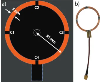
RF transmitter and receiver coils are used in MRI for generating a radio frequency signal and receiving MR signals. Basically, the simplest form of RF coils is a single loop. coil size plays an important role in sensitivity of the coil. Figure 3.1 shows the dimension of a single loop coil which we used in our design and the schematic of fabricated coil. C1 C2 C4 C3 5 mm 55 mm
a)
b)
Table 3.1 shows the values of matching and tuning capacitors which is extracted using Ansoft HFSS V. 13
C1 C2 C3 C4
45 pF 45 pF 45 pF 56 pF
Table 3.1: Matching and tuning capacitor values for the loop coil.
3.2
Power Dividers
Power dividers and power combiners are usable passive microwave components for diving and combining power. Power dividers divide input electromagnetic power into two or more ports for using in other circuits and power combiners collect power from two or more input ports into one port. Usually dividers with three-port networks divide power equally and create in-phase output powers are called power dividers, however the design of different ratios of division is possible.
3.2.1
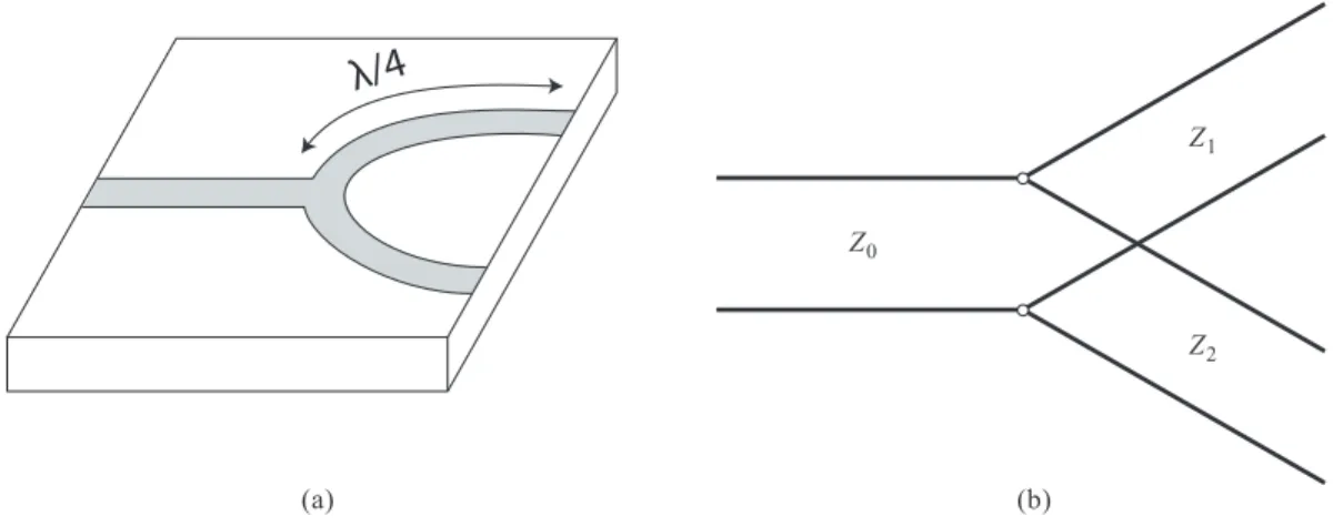
T-Junction Power Dividers
One of the earliest three-port network power dividers is T-Junction power divider. This divider can be modelled with three transmission lines as shown in Fig. 3.2. This network has low isolation between two output ports which allows power to flow between them. In order to solve this problem Wilkinson power dividers are used [31].
3.2.2
Wilkinson Power Dividers
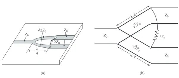
It can be easily shown that a three-port network cannot be lossless, reciprocal, and matched at all ports at the same time [31]. Wilkinson power divider is one of the important classes of power dividers which can provide strong isolation
Z1 Z2 Z0 ) b ( ) a (
λ/4
Figure 3.2: a) T-Junction Power divider and b) its lossless transmission line model.
between output ports while all the ports are matched. It is possible to design a Wilkinson power divider to divide the power equally or by a desired power ratio between output ports. Since it uses passive components, this network is a reciprocal network and also we can use it as a power combiner. Fig. 3.3 shows the microstrip form and circuit model of Wilkinson power dividers. Since we used a Siemens Magnetom 3 Tesla clinical MRI system with an eight channel parallel transmit array unit which operates at 123 MHz for our experiments, the wavelength is 2.439 m. Hence, a quarter wavelength is more than half a meter. Since we are using multiple dividers and combiners, microstrip form will consume a large area in the printed circuit board (PCB). Therefore, lumped-element Wilkinson power dividers and combiners are favorable.
3.2.2.1 Equal Wilkinson Power Divider
This section introduces a lumped element model of an equal Wilkinson power di-vider. Basically, a quadrature wave length can be modelled as a Pi- or T-network. Fig. 3.4 shows a lumped element model of an equal Wilkinson power divider which uses a LC Pi-network instead of quadrature wavelength transmission line [32].
/4 /4 4 Z0 2Z0 2Z0 Z0 Z0 Z0 2Z0 Z0 2Z0 2Z0 ) b ( ) a (
Figure 3.3: The Wilkinson power divider. a) An equal-split Wilkinson power divider in microstrip line form. b) Equivalent transmission line circuit.
cp Ls R Port 1 Port 2 Port 3 cp Ls 2cp
Figure 3.4: Schematic of the two-way lumped-element Wilkinson divider. Equations 3.1a and 3.1b show the value of capacitors and inductances accord-ing to the frequency and characteristic impedance of transmission line.
Cp = 1 2πf0Z0 = 1 2 × π × 123 × 106× 50 = 25.8 µf (3.1a) Ls= Z0 2πf0 = 50 2 × π × 123 × 106 = 64 nH (3.1b)
The proposed power divider with calculated component values is simulated using AWR Microwave Office and scattering parameters are extracted. The fab-ricated circuit is shown in Fig. 3.5. We measured scattering parameters of the circuit using an Agilent network analyzer. Measured and simulated matching parameters are compared in Table 4.1 and Fig. 4.2 shows the simulation results
and measurement results of scattering parameters.
Figure 3.5: Schematic of PCB circuitry of equal Wilkinson power divider.
3.2.2.2 Unequal Wilkinson Power Divider
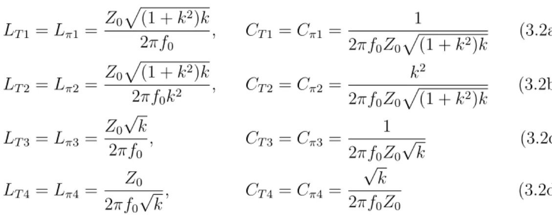
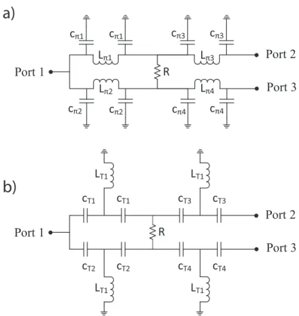
Closed form lumped element model of an unequal Wilkinson power divider with favorable division ratio is introduced in this section. Fig. 3.6 shows the equivalent circuit models of a Pi-network and T-network unequal Wilkinson power divider. Eqn. 3.2 show the value of elements for these two networks which have the same values. LT 1= Lπ1 = Z0p(1 + k2)k 2πf0 , CT 1 = Cπ1 = 1 2πf0Z0p(1 + k2)k (3.2a) LT 2= Lπ2 = Z0p(1 + k2)k 2πf0k2 , CT 2 = Cπ2 = k2 2πf0Z0p(1 + k2)k (3.2b) LT 3= Lπ3 = Z0 √ k 2πf0 , CT 3 = Cπ3 = 1 2πf0Z0 √ k (3.2c) LT 4= Lπ4 = Z0 2πf0 √ k, CT 4 = Cπ4 = √ k 2πf0Z0 (3.2d)
The dividing ratio of power between two output ports is known as k2. As we
discussed in Section 2.1 we used an unequal power divider with ratio of 9 to 1. Table 3.2 shows the value of capacitors and inductances according to the dividing ratio, frequency and characteristic impedance of transmission line.
cπ1 cπ1 cπ2 cπ2 cπ3 cπ3 cπ4 cπ4 Lπ1 Lπ2 Lπ3 Lπ4 R Port 2 Port 3 Port 1 cT1 cT1 LT1 R Port 2 Port 3 Port 1 cT3 LT1 cT3 cT2 cT2 cT4 cT4 LT1 LT1
a)
b)
Figure 3.6: Schematic of unequal lumped-elements Wilkinson power dividers a) using Pi-network b) using T-network.
Fig. 3.7 shows the PCB layout and PCB circuitry of designed Wilkinson power divider. Simulation results and measurement results of isolation parameters is shown in table 4.2. Simulation results and measurement results of scattering parameters is shown in Fig. 4.3
a) b)
L (nH) C (pF )
L1 L2 L3 L4 C1 C2 C3 C4
357 39 112 37 4.7 42 15 47
Table 3.2: Design values for unequal Wilkinson power divider.
3.3
Delay lines
3.3.1
Coaxial Cable
Coaxial cable is a transmission line with a negligible attenuation factor (Fig. 3.8). An electrical signal gets a fixed phase delay while getting transmitted through a coaxial cable. The phase delay increases with increasing the physical length of the coaxial cable. The wavelength according to the velocity factor of the coaxial
cable (Vf = 0.69) in our operating frequency is around 1.68 m.
Figure 3.8: Coaxial cable is used to create phase delay (photo courtesy of Wikipedia).
The phase delay between our transmit and receive coils due to geometrical de-coupling is approximately 150 degrees. As we discussed in Section 2.1 for decou-pling purpose we need 180 degrees delayed version of coudecou-pling signal. Therefore, a total of phase delay of 330 degrees is required. This amount of phase delay is achievable by using coaxial cable with a physical length of approximately 1.5 m. we used this approach in our 1-line design. However, long coaxial makes our
setup mechanically unstable and bulky. Therefore, instead of using coaxial cable we used phase shifters in our next design.
3.3.2
Phase Shifter
As we discussed in section 2.2 in four-line design we are using three fixed phase shifters of 90, 180 and 270 degrees. For this purpose we design lumped element model of phase shifters. It is well-known that every transmission line with
char-acteristic impedance of Z0 and propagation constant of β can be modelled with
two-port circuits [31]. Figure 3.9 shows T- and Pi-network models for trans-mission line and eqn 3.3a and 3.3b represent the ABCD Parameters of these networks.
Z1 Z2
Z3 Za Zb
Zc
a)
b)
Figure 3.9: Model of transmission line a) T-network b) Pi-network.
" A B C D # T = " 1 + Z1/Z3 Z1+ Z2+ Z1Z2/Z3 1/Z3 1 + Z2/Z3 # (3.3a) " A B C D # P i = " 1 + Z3/Z2 Z3 1/Z1+ 1/Z2+ Z3/Z1Z2 1 + Z3/Z1 # (3.3b)
The ABCD parameters of a transmission line can be written as follows: " A B C D # T ransmission line = " cos(βl) jZ0sin(βl) jsin(βl)/Z0 cos(βl) # (3.4)
by assuming that the desired port impedances are purely matched to Z0, equat-ing the ABCD parameters of Pi-network and T-network with ABCD parameters of transmission line, the value of elements for any desired phase is calculated. Equation 3.5a and 3.5b represent the value of impedances for T- and Pi-network phase shifters. Z1 = Z2 = −jZ0 cos(β) − 1 sin(β) Z3 = −j Z0 sin(β) (3.5a) Za = Zb = jZ0 sin(β) cos(β) − 1 Zc= jZ0sin(β) (3.5b)
Figure 3.10 shows a Pi-network 90-degrees phase shifter with values of ele-ments. we fabricated this 90-degrees phase shifter as it is shown figure
64 nH
25.8 pF 25.8 pF
Figure 3.10: Model of 90-degrees phase shifter.
C1 C2
L1
L2
P1 P2
a)
b)
In order to design 180 and 270-degrees phase shifters, we cascaded two and three 90-degrees phase shifters respectively. Figure 3.12 shows fabricated 180 and 270-degrees phase shifters.
a)
b)
Figure 3.12: PCB circuitry of phase shifter a) 180-degrees b) 270-degrees.
3.4
PIN diode variable RF attenuator circuit
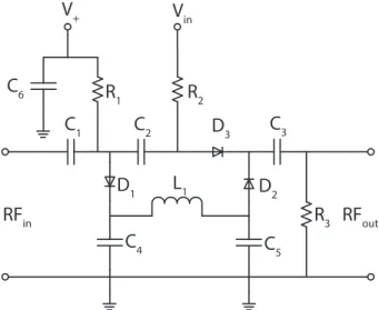
RF attenuators are RF devices which reduce the level of signal to the desired level. This device is widely used for different applications. For example in addition to reducing signal level, it can also improve the impedance matching specially in mixers or it can be used for controlling the level of output specially in RF gen-erators. There are different kinds of RF attenuators such as fix RF attenuators, switched RF attenuators and variable RF attenuators [33]. In our design we used PIN diode RF attenuator as it is shown in Fig. 3.13.
C6 C1 C2 D3 C3 R3 D2 C5 D1 C4 L1 R2 R1 RFin RFout V+ Vin
Table 3.2 shows the value of components for the proposed attenuator. The value of all capacitors are equal and by changing the input voltage up to 8 volt we can control the attenuation amount.
C L1 R1 R2 R3 Vin V+
50 pF 100 nH 2.2 KΩ 1 KΩ 2.7 KΩ 0 − 8 V 5 V
Table 3.3: Design values for PIN diode variable RF attenuator circuit.
The proposed PIN diode variable RF attenuator is shown in Fig. 3.14.
Figure 3.14: Schematic of PCB circuitry of PIN diode variable attenuator.
3.4.1
Digital Attenuator
We used a low-cost programmable digital 7-bit attenuator package (HMC759LP3E) in order to control our setup. This IC has the steps of 0.25 dB LSB Steps to 31.75 dB with a single supply of 5 V [29]. The schematic of applicable circuit of the attenuator IC is shown in Fig. 3.15. Communication protocol of this atten-uator IC is Serial Peripheral Interface Bus (SPI). In order to communicate with the attenuator IC we used a raspberry Pi [34]. Fig. 3.16 and Fig. 3.17 show the PCB top layer and bottom layer of fabricated attenuator IC and PCB circuitry of it.
Vdd1 1 SERIN 2 LE 3 CLK 4 PUP1 5 PUP2 6 SEROUT 7 RF1 8 ACG0 9 ACG1 10 ACG2 11 ACG3 12 RF2 13 GND 14 Vdd2 15 N/C 16 EP 17 U1 HMC759LP3E C8 100pF C2 10nF C4 10nF C5 10nF C3 10nF C9 1nF 1 2 5 6 3 4 7 8 9 10 11 12 13 14 15 16 17 18 19 20 21 22 23 24 25 26 P1 Vdd Vdd GND GND GND LE GND GND SERIN SEROUT CLK CLK Vdd GND SEROUT SERIN LE GND R1 39k C10 4.7uF Vdd GND R2 39k R3 39k R4 39k Vdd Vdd SEROUT Vdd RF1 GND GND GND C6 10nF GND C1 10nF RF2 C7 100pF GND 5 1 2 3 4 J1 5 1 2 3 4 J2 RF1 RF2 G N D G N D G N D G N D GN D GN D GN D GN D GND GND
Figure 3.15: Schematic of applicable circuit of HMC759LP3E
to send attenuation factor via SPI to the attenuator IC. We set the attenuator IC to different attenuation values.
Top Layer Bottom Layer
a)
b)
Figure 3.16: a) Top layer b) bottom layer of fabricated attenuator IC.
Figure 3.17: PCB circuitry of attenuator IC
3.5
Geometric Decoupling
In order to geometrically decouple transmit and receive coils as much as possible, we test different angles between the transmit and receive coils. As a result the coils should be placed orthogonally to each other. Therefore we placed the coils orthogonally using a setup which has three freedom degrees for aligning the coils (Fig. 3.18)
Figure 3.18: Schematic of setup which we used in order to place two coils or-thogonal to each other. This setup has three degree of freedom for changing the position of two coils with respect to each other.
3.6
Semi-Automatic
Controllable
Decoupling
Design
Fig. 3.19 shows our semi-automatic controllable decoupling setup. In this setup as we discussed in Section 2.1 an unequal Wilkinson power divider is used to divide the input power between transmit coil and delay and attenuator line. Actually for maintaining power efficiency the transmit coil is fed by 90% of the power and 10% of the power is passing through the delay and attenuator line. In this design we used coaxial cables for creating desired phase delay. The attenuator IC is connected to the coaxial cable and we control it using our optimization algorithm. A Raspberry Pi 2 Model B is used for getting attenuator states from MATLAB and sets the attenuator IC. At the output a Wilkinson power combiner is used for combining power from the output of attenuator and receiver coil.
Figure 3.19: Schematic of semi-automatic controllable decoupling setup including geometric decoupling.
3.7
Fully-Automatic Controllable Decoupling
Design
In this design as we discussed in Section 2.1, an unequal Wilkinson power divider is used to feed the cancellation circuit and transmit coil. There are three equal Wilkinson power divider in the cancellation circuit in order to feed each attenuator and delay line. Since we want to use 0 degree phase shifter, in the first line we do not have any phase shifter. In line 2, 3 and 4 we have three phase shifters which are producing 90, 180 and 270 degrees as delay lines. Each line is connected to a programmable attenuator IC and then using three Wilkinson power combiners, the signal which is required for decoupling is created. At the end this signal is added to the receive signal which is detected by the receive coil.Fig. 3.20 shows the schematic of our fully-automatic controllable decoupling design design. The PCB circuitry of this design is shown in Fig. 3.21. In this circuit we matched all the lines to 50 Ω.
Modulator Tx-Chain Syntesizer Power Amplifier Gain =15dB NF=3dB Receiver ULNA Gain=25 NF=1dB Network Analyzer Φ=0° Φ=90° Φ=180° Φ=270° A# R x -C o il Tx-Coil Phantom Control Communica$on Interface -10dB -0.45dB Unequal Power Divider
-3dB -3dB -3dB -3dB -3dB -3dB -3dB Power Combiner A# A# A#
Phase Shi%ers A#enuators Power Combiners
Power Dividers
Figure 3.20: Schematic diagram of proposed method based on geometric decou-pling and active decoudecou-pling with 4-lines of delay and attenuator using full duplex radio system. In this part we used four fixed-delay lines for stimulating phase delay.
Figure 3.22: Schematic of fully-automatic controllable decoupling setup including geometric decoupling.
Chapter 4
Experimental Results
In this chapter, the results of designed RF circuits as well as the decoupling and MRI experiment outcomes of the coupling cancellation designs are presented.
4.1
RF Coils
Simulation results and measurement results of S11parameter for our designed RF
loop coil are shown in Fig. 4.1. Both magnitude and phase of S11 in measurement
results are in good agreement with the simulation results.
a)
b)
4.2
Power Dividers
The proposed equal and unequal Wilkinson power dividers with calculated com-ponent values are simulated using AWR Microwave Office and scattering param-eters are extracted. We measured scattering paramparam-eters of the circuit using an Agilent network analyzer.
4.2.1
Equal Wilkinson Power Divider
Measured and simulated matching parameters for the equal Wilkinson power divider are compared in Table 4.1. Fig. 4.2 shows the simulation results and measurement results of scattering parameters.
S11 (dB) S22 (dB) S33 (dB)
Simulation -11 -17 -18
Measurement -9.8 -12.3 -15.6
Figure 4.2: Simulation and measurement results of unequal power divider.
4.2.2
Unequal Wilkinson Power Divider
Simulation results and measurement results of isolation parameters of the un-equal Wilkinson power divider is shown in table 4.2. The mismatch between the measurement and simulated results are due to using standard values instead of calculated values for inductors and capacitors. Simulation results and measure-ment results of scattering parameters is shown in Fig. 4.3.
S11 (dB) S22 (dB) S33 (dB)
Simulation -40 -42 -35.3
Measurement -13.67 -12.6 -16.3
Table 4.2: Simulated and measured S-parameters for unequal Wilkinson power divider.
100 105 110 115 120 125 130 135 140 145 -60 -50 -40 -30 -20 -10 0 10 S -P a r a m e t e r s ( d B ) Frequency (MHz) S12-AW R S13-AW R S23-AW R S12-measurment S13-measurment S23-measurment
Figure 4.3: Simulation and measurement results of unequal power divider.
4.3
Delay lines
We have designed fixed phase shifters to act as the required fixed delay lines in the fully-automatic controllable decoupling design.
4.3.1
Phase Shifter
Figure 4.4 shows the simulation and measurement results of the fabricated phase shifters for 90, 180 and 270 degrees. The slight mismatch between simulation results and measurement results is due to using standard values for capacitors and inductors instead of actual calculated values.
95 100 105 110 115 120 125 130 135 140 145 150 -450 -400 -350 -300 -250 -200 -150 -100 -50 P h a s e o f S 1 2 ( d e g r e e s ) Frequency (MHz) 90 degree-measurement 90 degree-Simulation 180 degree-measurement 180 degree-Simulation 270 degree-measurement 270 degree-Simulation
Figure 4.4: Simulation and measurement results of the fabricated phase shifters for 90, 180 and 270 degrees.
4.4
Attenuators
The simulation and measurement results of analog variable RF attenuator de-signed using PIN diodes and digital attenuator IC are presented in this section.
4.4.1
PIN diode variable RF attenuator circuit
We measured the magnitude and phase of S12 of the attenuator. Figure 4.5 shows
the measurement results of S12 parameter. According to Fig. 4.5b phase of S12
shifts from 40 degrees to -40 degrees by changing the input voltage. Since in our design the phase delay of each line should be fixed, the change in the phase of
S12 of the attenuator negatively affects the result of our design. Therefore, we
could not use this attenuator. In order to solve this problem, we used a digital attenuator IC (HMC759LP3E) which will be discussed in the next section [29].
4.4.2
Digital Attenuator
The magnitude and phase of S12 for the attenuator IC is plotted in Fig. 4.6 for
different set values. The attenuation varies from approximately -35 dB to -3.5 dB in 128 steps. The change in phase delay for the attenuator IC is much smaller than the PIN diode variable attenuator. However, the slight shift in phase delay of the attenuator IC brings some limitation in decoupling the coils further since we expect the phase delay to be zero for the attenuators in each line and delay the signals using phase shifters only.
a)
b)
Figure 4.5: a) Magnitude b) phase of measured S12 of PIN diode analog
a)
b)
Figure 4.6: a) Magnitude of S12 of attenuator IC b) Phase of measured S12 of
attenuator IC. The phase of attenuator IC is changed and it is negatively affect our design.
4.5
Geometric Decoupling
The simulation results of the geometrical decoupling of the coils for different angles between the transmit and receive coils are done in HFSS and plotted in Fig. 4.7. Since the best decoupling is when the angle between the two coils is 90
degrees, we placed the coils orthogonal to each other and measured its S12 using
a network analyzer. The measurement result of the geometrical decoupling for the orthogonal case is illustrated in Fig. 4.8.
Figure 4.7: Magnitude of S12 with respect to the coils angle. This figure shows
that the best decoupling amount is achieved when two coils are placed orthogonal to each other.
a) b)
Figure 4.8: a) Magnitude b) phase of measured S12 of transmit and receive coils
which are placed orthogonal to each other
4.6
Semi-Automatic
Controllable
Decoupling
Design
For the MRI experiment, firstly using network analyzer we measured the
ampli-tude of S12 of the output signal as a feedback for our algorithm and minimized
that with tuning of the attenuation factor. Then we put the setup inside MRI and again we tried to optimize the circuit to get the best decoupling amount in-side the magnet. Fig. 4.9 shows the achieved decoupling amount inin-side the MRI magnet using our 1-line design.
-90 -45 0 45 90 |S 12 | -80 -70 -60 -50 -40
Figure 4.9: Amount of decoupling measured using network analyzer inside MRI magnet.
We used a Siemens Magnetom 3 Tesla clinical MRI system with an eight channel parallel transmit array unit which operates at 123 MHz. Fig. 4.10 shows the raw-data for CEA with a CuSO4(aq) phantom. The oscillations due to the MR signal response are already visible without any data processing. Note that the first 4 points of the each acquired radial spoke were neglected in reconstruction since the data was deformed by the ADC filtering effects. Missing points were interpolated using the consecutive points. Fig. 4.11 shows a deconvolved MR signal response from the rubber phantom. Post processing of the data is done by
our colleague, Ali C¸ a˘glar ¨Ozen, at Freiburg University.
0.0 0.2 0.4 0.6 0.8 1.0 1.2 1.4 1.6 1.8 2.0 0.5 1.0 Amplitude Phase T ime (ms) A m p l i t u d e ( m V ) -100 -50 0 P h a s e ( R a d i a n s )
Figure 4.10: Phase and amplitude of the unprocessed CEA MR signal from a CuSO4(aq) sample. Decoupling is linearly dependent on frequency and shows a minima at the center frequency. Spins get excited as soon as the resonance conditions are satisfied during the linear frequency sweep. Cf. Methods section for imaging parameters.
Figure 4.11: Real part of the deconvolved CEA response from a rubber sample, acquired with a chirp RF pulse of 32 kHz sweep range over 2 ms. Cf. Methods
section for imaging parameters. The post processing is done by Ali C¸ a˘glar ¨Ozen.
4.7
Fully-Automatic Controllable Decoupling
Design
We did our experiments in a Siemens Magnetom 3 Tesla clinical MRI system with an eight channel parallel transmit array unit which operates at 123 MHz. Firstly, we put the setup into the MR magnet and connected the circuit to the control PC using a Raspberry Pi. An Agilent network analyzer was used to calculate the decoupling of the setup which was then fed to the genetic algorithm based optimization software written in MATLAB to find the best attenuation factors of all the lines and achieve the highest decoupling value. Fig. 4.12 illustrates the decoupling measured using network analyzer.
The setup was connected to the MRI system. 64 kHz chirp pulse was swept over 2 ms and the acquired signal was processed as described in [5]. The signal processing steps and the resulting spin response is shown. Fig. 4.13 shows the acquired signal from a rubber phantom, Fig. 4.14 shows the MR signal after leakage subtraction, and Fig. 4.15 shows deconvolved spin response.
-20 -10 0 10 20 |S 1 2 (dB)| -110 -100 -90 -80 -70 -60
Figure 4.12: Amount of achievable decoupling using our coupling cancellation circuit measured with network analyzer.
0.0 0.2 0.4 0.6 0.8 1.0 1.2 1.4 1.6 1.8 2.0 0 5 10 15 20 25 30 Amplitude Phase T ime (ms) A m p l i t u d e ( m V ) -40 -20 0 20 40 60 80 100 P h a s e ( R a d i a n s )
0.0 0.2 0.4 0.6 0.8 1.0 1.2 1.4 1.6 1.8 2.0 0 1 2 3 4 5 6 Amplitude Phase T ime (ms) A m p l i t u d e ( m V ) 0 5 10 15 20 25 30 35 40 45 50 55 60 65 P h a s e ( R a d i a n s )
Figure 4.14: MR signal after leakage subtraction.
0.0 0.2 0.4 0.6 0.8 1.0 1.2 1.4 1.6 1.8 2.0 0 500 1000 1500 2000 Amplitude Phase T ime (ms) A m p l i t u d e ( V ) -400 -300 -200 -100 0 P h a s e ( R a d i a n s )
Chapter 5
Discussion
Our design which is basically an analog cancellation circuit, while an important step forward, leaves several important new possibilities and future research. In this chapter we want to briefly discuss some of them.
As we discussed in section 2.2, we need at least four lines consisting of a phase delay and an attenuator. In the mathematical approach that we discussed, the fixed phase delays are just created by the phase shifters. We have neglected the effect of the PCB tracks and other parts of the circuit such as attenuators and power dividers and combiners on the phase delay of each line. In the real case, each component adds an error to the phase delays and limits the maxi-mum achievable decoupling. The attenuator IC that we have used has discreet available attenuation amounts. The phase delay caused by this IC varies from 5 to 20 degrees for different attenuation amounts. This affects the limitation on the maximum achievable decoupling which will be dependent on the phase delay of the coils caused by geometrical decoupling. In addition, discretization of ICs causes some drawbacks. For instance, for a special case, the attenuation of the two active lines should be 5.74 and 13 dB. But since the ICs cannot provide these exact attenuation amounts and the ICs have 0.25 dB step size, the decoupling provided by the circuit is limited. Fig. 5.1 shows amount of decoupling for the nearest possible attenuation states to the desired circuit state. Even a very small
deviation from the best case decreases the amount of decoupling significantly.
Figure 5.1: Amount of decoupling for the four nearest possible attenuation states to the desired circuit state. a=-5.7494 dB and b=-13 dB are the exact required attenuation amounts.
We simulated the limitation on the maximum achievable decoupling caused only by the discretization of attenuator ICs using a MATLAB code. Fig. 5.2 shows the maximum achievable decoupling versus the phase delay of the coils. In some phase delay values, the ICs can provide attenuation states that has a very small deviation from the desired values and we can achieve higher decoupling amounts. Our circuit guarantees at least 60 dB of decoupling for every arbitrary phase delay. By adjusting the phase delays, we can achieve more than 100 dB decoupling.
Figure 5.2: Maximum achievable decoupling versus the phase delay of the coils. This design guarantees at least 60 dB of decoupling for every arbitrary phase delay and by adjusting the phase delays, we can achieve more than 100 dB decoupling. which is also practical for multiple input multiple output (MIMO). One can use the same design for transmit and receive array systems in CEA MRI applications. However, the key challenge is that for using N transmit chains N2 cancellation circuit is needed to achieve the same decoupling amount. The second point is that transmit coils should properly decoupled from each other by using capasitive decoupling techniques
There is no feedback from MRI in our current prototype while CEA MRI is running. First, the circuit is tuned using network analyzer inside the MRI. Then, the network analyzer is disconnected from the circuit while we start the imaging without any feedback. This approach is suitable for static environments as well as dynamic environments with small changes over time. In order to make this
design applicable for in vivo experiments and dynamic situations, a real-time feedback is required from the MRI scanner during the imaging. One can get the MRI signal before the reconstruction process, analyze it, and calculate the attenuation constants by solving the inverse problem of the system instead of the optimization algorithm. This process should be fast enough to be done between every two consecutive MRI signal pulses.
Chapter 6
Conclusion
This thesis presents a new method to decouple transmit and receive coils for con-current excitation and acquisition (CEA) in MRI. The proof-of-concept demon-stration of using automatically controllable decoupling circuits for CEA and
get-ting images from tissues with very short T2 time is done in this study. This
study shows that the RF coupled signal in the receiver coil is reduced more than more than 100 dB using our proposed method. This method consist of geo-metrical decoupling and automatically controlled decoupling design for getting
images from tissues with very short T2 relaxation time. We implemented the
automatically controlled decoupling method using two designs: Semi-automatic and fully-automatic controllable decoupling designs. In the proposed method, cancellation circuit can automatically tune itself using a genetic algorithm opti-mization and provides favorable decoupling for CEA purposes. We demonstrated more than 100 dB decoupling using both designs and run MRI experiments using a clinical 3 Tesla MRI system with parallel transmit array to get images of a rubber phantom.
Bibliography
[1] “Knee mri image.” http://www.freitasrad.net/pages/Basic_MSK_MRI/ Knee.htm.
[2] P. Gatehouse and G. Bydder, “Magnetic resonance imaging of short T 2 components in tissue,” Clinical radiology, vol. 58, no. 1, pp. 1–19, 2003. [3] D. J. Tyler, M. D. Robson, R. M. Henkelman, I. R. Young, and G. M. Bydder,
“Magnetic resonance imaging with ultrashort TE (UTE) PULSE sequences: technical considerations,” Journal of Magnetic Resonance Imaging, vol. 25, no. 2, pp. 279–289, 2007.
[4] D. O. Kuethe, A. Caprihan, E. Fukushima, and R. A. Waggoner, “Imaging lungs using inert fluorinated gases,” Magnetic resonance in medicine, vol. 39, no. 1, pp. 85–88, 1998.
[5] D. Idiyatullin, S. Suddarth, C. A. Corum, G. Adriany, and M. Garwood, “Continuous SWIFT,” Journal of Magnetic Resonance, vol. 220, pp. 26–31, 2012.
[6] D. Bharadia, E. McMilin, and S. Katti, “Full duplex radios,” in ACM SIG-COMM Computer Communication Review, vol. 43, pp. 375–386, ACM, 2013. [7] E. M. Purcell, H. Torrey, and R. V. Pound, “Resonance absorption by nuclear magnetic moments in a solid,” Physical review, vol. 69, no. 1-2, p. 37, 1946. [8] H. Torrey, “Transient nutations in nuclear magnetic resonance,” Physical
[9] A. J. Fagan, G. R. Davies, J. M. Hutchison, and D. J. Lurie, “Continu-ous wave MRI of heterogene“Continu-ous materials,” Journal of Magnetic Resonance, vol. 163, no. 2, pp. 318–324, 2003.
[10] A. J. Fagan, G. R. Davies, J. M. Hutchison, F. P. Glasser, and D. J. Lurie, “Development of a 3-D, multi-nuclear continuous wave NMR imaging sys-tem,” Journal of Magnetic Resonance, vol. 176, no. 2, pp. 140–150, 2005.
[11] M. Weiger, D. O. Brunner, B. E. Dietrich, C. F. M¨uller, and K. P.
Pruess-mann, “ZTE imaging in humans,” Magnetic resonance in medicine, vol. 70, no. 2, pp. 328–332, 2013.
[12] M. Weiger, D. O. Brunner, M. Tabbert, M. Pavan, T. Schmid, and K. P. Pruessmann, “Exploring the bandwidth limits of ZTE imaging,” signal, vol. 1, no. 2, p. 3, 2013.
[13] M. Weiger and K. Pruessmann, “MRI with zero echo time,” eMagRes, 2012. [14] M. Weiger, K. P. Pruessmann, and F. Hennel, “MRI with zero echo time: hard versus sweep pulse excitation,” Magnetic resonance in medicine, vol. 66, no. 2, pp. 379–389, 2011.
[15] D. O. Kuethe, A. Caprihan, I. J. Lowe, D. P. Madio, and H. M. Gach, “Trans-forming NMR data despite missing points,” Journal of Magnetic Resonance, vol. 139, no. 1, pp. 18–25, 1999.
[16] D. Brunner, M. Pavan, B. Dietrich, D. Rothmund, A. Heller, and K. Pruess-mann, “Sideband excitation for concurrent rf transmission and reception,” in Proceedings of the 19th Annual Meeting of ISMRM, Montreal, Quebec, Canada, p. 625, 2011.
[17] R. K. Gupta, J. A. Ferretti, and E. D. Becker, “Rapid scan Fourier transform NMR spectroscopy,” Journal of Magnetic Resonance (1969), vol. 13, no. 3, pp. 275–290, 1974.
[18] D. Idiyatullin, C. Corum, S. Moeller, and M. Garwood, “Gapped pulses-MRI,” Journal of Magnetic Resonance, vol. 193, no. 2, pp. 267–273, 2008.
![Figure 1.1: a) X-Ray and b) MRI images of knee [1] (used with permission).](https://thumb-eu.123doks.com/thumbv2/9libnet/5760027.116500/20.918.267.698.435.769/figure-x-ray-mri-images-knee-used-permission.webp)