Self-aligned via and trench for metal contact in III-V semiconductor devices
Jun Fei Zheng, Hilmi Volkan Demir, Vijit A. Sabnis, Onur Fidaner, James S. Harris, and David A. B. Miller
Citation: Journal of Vacuum Science & Technology B: Microelectronics and Nanometer Structures Processing, Measurement, and Phenomena 24, 1117 (2006); doi: 10.1116/1.2188000
View online: http://dx.doi.org/10.1116/1.2188000
View Table of Contents: http://avs.scitation.org/toc/jvn/24/3 Published by the American Institute of Physics
Engineering, Bilkent University, Bilkent, 06800 Ankara, Turkey
Vijit A. Sabnis, Onur Fidaner, James S. Harris, Jr., and David A. B. Miller
E.L. Ginzton Laboratory, Stanford University, Stanford, California 94305
共Received 10 November 2005; accepted 24 February 2006; published 21 April 2006兲
A semiconductor processing method for the formation of self-aligned via and trench structures in III-V semiconductor devices共in particular, on InP platform兲 is presented, together with fabrication results. As a template for such self-aligned via and trench formations in a surrounding polymer layer on a semiconductor device, we make use of a sacrificial layer that consists of either a SiO2dielectric hard mask layer deposited on the device layers or a sacrificial semiconductor layer grown on top of the device epitaxial layers共e.g., InP on an InGaAs etch stop兲, both laid down on the device layers before patterning the device geometry. During the semiconductor device etching, the sacrificial layer is kept as a part of the patterned structures and is, therefore, perfectly self-aligned. By selectively removing the sacrificial layer surrounded by the polymer that is etched back within the thickness of the sacrificial layer, an opening such as a via and a trench is formed perfectly self-aligned on the device top area in the place of the sacrificial layer. This process yields a pristine semiconductor surface for metal contacts and fully utilizes the contact area available on the device top, no matter how small the device area is. This approach thus provides as low an Ohmic contact resistance as possible upon filling the via and the trench with metal deposition. The additional use of a thin Si3N4 protecting layer surrounding the device sidewalls improves the robustness of the process without any undesired impact on the device electrical passivation共or on the optical mode characteristics if the device also includes a waveguide兲. This method offers metal contacts scalable to the device size, being limited only by the feasible device size itself. This method is also applicable to the fabrication of other III-V based integrated devices. © 2006 American Vacuum Society.
关DOI: 10.1116/1.2188000兴
I. INTRODUCTION
In III-V semiconductor technology, devices are typically fabricated vertically from layered epitaxial materials, where the device top commonly serves as the contact area for metal interconnection. As the devices are scaled down for high-speed operation, it becomes critically important to utilize as large a contact area as possible on the device top for the metal-semiconductor contact so as to achieve a low contact resistance. The traditional approach for making contacts is to etch a via structure through a polymer layer surrounding the III-V devices.1In this case, the via is normally smaller than the device due to the need for a lithography alignment mar-gin. The alignment margin, which is optically and mechani-cally limited, cannot be further scaled down when the device size is smaller than a certain limit, thus undesirably keeping the via to be a small fraction of the available total device area. Alternative approaches have been used to planarize a polymer film to the device top and use a non-self-aligned metal pad larger than the device for making contact.2,3This approach, however, depends on the ability to planarize the
polymer to level the device top so that the metal does not make contact to the device sidewalls. Not contacting the sidewalls is critical for vertically made layered devices that are sensitive to current leakage and short circuiting on the sidewall. Also, this method would take larger chip area than necessary between devices due to the margin needed for the top non-self-aligned metal pads, in some cases limiting much-needed tight integration between devices, e.g., for short distance interconnects.
In a typical polymer planarization process, for example, with benzocyclobutene 共BCB兲,4 the polymer is spun on the entire wafer. Usually this polymer film is so thick that the underlying device height variation will have minimum im-pact and a planarized polymer top will be achieved. The polymer is then subsequently etched back so that the etched polymer surface is level with that of the devices, allowing the device top to be used for contacts. In so doing, difficul-ties may arise, especially in wafer-level integrated process-ing, due to nonuniformities of the spin-on polymer thickness and the etch rate of the polymer across the wafer. Addition-ally, for example, in the case of monolithic integration, any device height variation due to epitaxial regrowth processes5,6 can also lead to the nonplanarization of the polymer on de-vices across an integrated chip and/or the whole wafer. In
a兲Author to whom correspondence should be addressed; electronic mail:
such cases, the exposure of device sidewalls becomes an unavoidable problem in any attempt to clear the polymer from all of the device tops. As a remedy to this problem, a quasiplanarization technique was introduced, which allows for the localized planarization of the device top with the polymer in the close vicinity of the device.7 However, this technique relies on an a priori anisotropic semiconductor wet etch process to create an undercut structure beneath the dielectric hard mask used for defining the device mesa. In this technique, it is difficult to control the device dimensions after the anisotropic etch, and such control is especially criti-cal for the devices with dimensions comparable to the under-cut created共typically micrometers in size兲. The micron-scale undercut structure further limits the tight integration of two adjacent devices, thus imposing a severe constraint on how closely they can be integrated on a chip; the undercut margin will keep the devices away from each other, creating a prob-lem similar to that introduced by a non-self-aligned large metal pad, as discussed above.
In this article, we introduce a self-aligned via and trench formation method that allows for the full utilization of the device top for making metal contacts. Providing self-alignment for metallization, we avoid the limitations to tight integration found in previously reported methods. The method eliminates the need for precision lithography for highly accurate alignment of the via. The method yields a pristine surface for making metal-semiconductor contacts. The method is also robust for the wafer-level integration and is insensitive to the aforementioned nonuniformities of spun-on polymer thickness, etch nonuniformity, and device height variation. In Sec. II, we start with presenting the implementation details of the method. In Sec. III, we discuss the application of the method to an InP-based on-chip gration of mesa and waveguide devices for photonic inte-grated chips, with more advanced and optional variations of
the basic method to elaborate the full advantages of the method and its robustness. Finally in Sec. IV, we conclude with a discussion regarding possible future applications.
II. APPLICATION OF THE METHOD
The key steps in the process of self-aligned via formation are illustrated in Fig. 1: 共a兲 A hard mask is formed using conventional dielectric thin film deposition, transfer lithogra-phy patterning, and etching. This hard mask is required to be thick enough to compensate for the differences in device height, the variation in spin-on polymer thickness, and the nonuniformity in polymer etch back.共b兲 III-V semiconductor is etched by reactive ion etching共RIE兲 using the hard mask to define the device. 共c兲 Subsequently, a spin-on polymer layer is spun and etched back to stop within the hard mask for every single device across the wafer.共d兲 The hard mask is later removed by wet etching, leaving a via structure and a pristine semiconductor surface for metallization. Note that this method can also be applied to generate a trench struc-ture, for example, to be used to metallize the top of a wave-guide device such as an electroabsorption modulator共EAM兲. In this process, it may be difficult to deposit and pattern thick layers of the dielectric to be used as the hard mask, as dielectric films of micrometers in thickness will introduce an inability to adhere to the wafer and inaccuracy in the lithog-raphy pattern transfer process, especially for very small fea-ture sizes down to 100 nm or below. Moreover, the stress within such a dielectric film can be so high that high-aspect-ratio hard mask features will peel off mostly because of the relatively higher stress in thick film and the weak adhesion of the dielectric film to small III-V semiconductor structures. To render the process robust in this sense, a sacrificial semi-conductor material could be added to the very top in the epitaxial layer design. The sacrificial semiconductor is typi-FIG. 1. Schematics of the self-aligned via 共and trench兲 formation process using a hard mask as a template. 共a兲 The hard mask is formed on the III-V
semiconductor.共b兲 The semiconductor is etched to define the active device area. A proper etch method is used to avoid undercut. 共c兲 Retaining the hard mask, a self-planarizing polymer layer is spun and etched back to stop within the thickness of the hard mask.共d兲 The hard mask is removed to form a self-aligned via共and trench兲 opening.
FIG. 2. Schematics of the self-aligned via共and trench兲 formation process using sacrificial InP epitaxial material, with InGaAs as an etch-stop layer. 共a兲 The hard mask is used to etch the mesa, including the sacrificial layer.共b兲 The hard mask is removed. The structure may be protected against wet etch as necessary by covering the wafer surface with a thin Si3N4layer.共c兲 A thick polymer layer is spun and etched back to stop within the sacrificial layer. 共d兲 The sacrificial
layer is selectively wet etched. The etch-stop layer helps render a flat surface, protecting the epitaxial layers beneath. In can be removed using a subsequent selective wet etch, or the etch stop can be retained as the contact layer.
1118 Zheng et al.: Self-aligned via and trench for metal contact 1118
quently, an accurate pattern transfer is also assured.
This process flow is illustrated in Fig. 2. The sacrificial layer is patterned with the device layers beneath it. The di-electric hard mask is removed using a wet etch. The device structure surface is optionally protected by a layer such as a thin Si3N4 layer, which may be necessary to prevent the de-vice structures from being etched away during the subse-quent wet etch removal of the sacrificial semiconductor layer. The polymer is then spun in a similar way as described before and the etch back is stopped within the sacrificial semiconductor layer in this case. Then, the sacrificial layer is selectively removed using a wet etch, with the etch-stop layer between the sacrificial layer and the device layers un-derneath. This forms a via in place of the sacrificial layer. This variation of our method has a number of advantages similar to those of the dielectric hard mask based approach: 共i兲 The sacrificial layer is deposited conveniently during ep-itaxial growth and can be grown as thick as necessary to accommodate the nonuniformities and to achieve deep enough vias, e.g., as deep as 1m.共ii兲 The optional sidewall protection is used during the selective wet removal of the sacrificial layer, allowing increased robustness.共iii兲 Since the sacrificial layer is epitaxially grown, it has good adhesion to the contact material beneath to avoid delaminating from it. 共iv兲 Also, after the removal, it does not leave any dielectric remnant that would increase the contact resistance.
III. RESULTS AND DISCUSSION
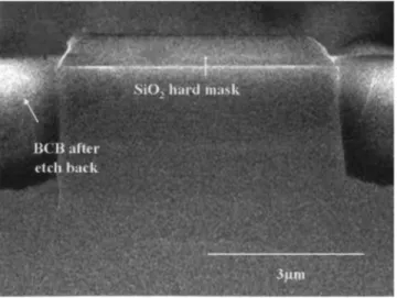
We employed this method to integrate InP-based wave-guide and mesa structures into photonic integrated switches. In the demonstration of a simple process as illustrated in Fig. 1, a SiO2 hard mask was used along with a BCB polymer layer2 for the via formation. Figure 3 shows the cross-sectional scanning electron microscope共SEM兲 image of one
terning the SiO2 film to form a hard mask, RIE was used to remove InP from the unprotected areas to obtain 3m high waveguide ridges 共4 m wide兲. Thick BCB polymer layer was spun to yield a 9 – 10m thick film after curing to achieve a uniformity of ±0.1m 共excluding an edge of about 2 mm wide兲. For the etch back, we used a fast etch recipe with an etch rate of 1.4– 1.6m / min and a consecu-tive slow etch recipe with an etch rate of 0.4– 0.6m / min. During the polymer etch back, the thickness of the remaining BCB film could also be monitored using an in situ laser monitor. To ensure that the etch stops within the SiO2 film for all devices across the wafer, the RIE can be ran with additional periodic examinations of the wafer under an opti-cal microscope. We could verify that all of the device tops were cleared by looking for the reappearance of the uniform color of the original SiO2 film at its deposition thickness of 0.75m. Residual BCB on the SiO2hard mask will cause a variation of colors due to thin film reflection and interfer-ence. Once the device tops are open, the SiO2hard mask can easily be etched away by an approximately 1 min dip in 6:1 BOE. Consequently, the resulting via is conveniently self-aligned.
From Fig. 3, we notice that the sidewalls of the SiO2hard mask are sloped. This slope is due to the dielectric etch used to pattern the hard mask. By improving the SiO2 RIE etch process, the sidewalls can be made straighter. However, this sloped profile can also be advantageous because it makes the BCB-SiO2 interface tilted, which prevents vertically travel-ing ions from getttravel-ing into the BCB-SiO2interface. Such un-desired penetration of the ions can sometimes result in the so called microtrenching, an etch-enhanced separation of BCB from the SiO2 or even the InP device beneath it.7
Figure 4 shows the atomic force microscope 共AFM兲 top view image of a large共30⫻30m2兲 via after the removal of the hard mask. The zoomed image of the surface demon-strates that we can create a pristine surface after the removal of the hard mask. The exposed device surface is a p+ contact InGaAs layer, which is atomically flat, except for atomic step
FIG. 3. Cross-sectional SEM image of devices during self-aligned via for-mation process steps.
FIG. 4. Atomic force microscope image of a 30⫻30m2self-aligned via
opening formed after wet etch removal of the SiO2hard mask. A zoomed
image 共on the right兲 of a very small area reveals that a pristine InGaAs surface with clearly visible atomic steps is achieved.
features coming from the substrate cut and epitaxial growth. The clear atomic steps in the AFM image indicate that no residue of either SiO2 or BCB is left on the surface. Note that, in the conventional polymer etch-back method, in which the dielectric hard mask is not retained during the polymer etch, polymer residues usually remain on the top surface due to the difficulty of completely removing the very last polymer on the device surface without overetching the polymer surrounding the device. Also, hydrocarbon molecu-lar deposits may be formed on the device top surface during plasma bombardment or due to heating effect. Such a clean surface obtained using our method allows for very low Ohmic contact resistance. For example, we fabricated diodes and made Ohmic contacts on the diode surfaces prepared by removing SiO2to achieve contact resistances of 15.3± 3.2⍀ in 30⫻30m2device area.7
In our second demonstration, we employed an InP sacri-ficial layer beneath the SiO2hard mask for the formation of a trench to be used during the metallization of a waveguide structure. In the epitaxial layer design, we used a 50 nm thick InGaAs layer under the sacrificial InP layer to serve as a wet etch stop during subsequent InP removal. InGaAs can be allowed to remain in the structure after InP sacrificial layer removal because it can be conveniently used also as the
p+ contact layer. A SiO2 hard mask is used, as before, to
define the waveguide ridge. After defining the waveguide, the SiO2 is removed using the BOE etch. The whole struc-ture after SiO2 removal is, however, protected by the Si3N4 thin film deposited before spinning BCB.
This Si3N4 thin film has a twofold use: first, it protects any portion of the sidewalls of the devices from exposure to the wet chemical used during the removal of InP sacrificial materials, if the sidewalls are excessively exposed as a result of overetching the polymer BCB or as a result of having device structures nonuniform in height. The reason for the choice of the Si3N4 film stems from its high resistance to strong acidic wet chemical, as in the case of InP removal, for which we used 1:3 HCl: H3PO4mixture. Second, the silicon nitride film protects the device from metal depositing onto device sidewalls in any area where BCB delaminates from the InP device because of the so called microtrenching. Such microtrenching is due to the enhancement of the BCB etch at the delaminated interface by the vertically traveling ion bom-bard during the BCB etch-back process as reported in Ref. 7 and shown in Fig. 5. The Si3N4film adheres very well to the sidewalls of an InP device, so the existing Si3N4 strongly protects the sidewall from undesired metal shorting phenom-ena. The process steps after Si3N4coating are as follows:共1兲 we spin, cure, and etch back the BCB film; and共2兲 the Si3N4 protection coating on top of the sacrificial InP is then easily etched away during the BCB etch back because it is very thin as discussed later, opening the surface of the sacrificial InP for its subsequent etch removal. The InP sacrificial layer after top Si3N4removal is shown in Fig. 5, similar to that previ-ously illustrated in Fig. 2共c兲. Here Fig. 5 shows a SEM im-age of the structure during the process steps with a 1000 Å thick Si3N4 layer covering the sidewall of the structure be-fore the InP sacrificial layer is removed. Figures 6共a兲 and 6共b兲 show the cross-sectional SEM views of the trench over an InP-based waveguide diode after the removal of the sac-rificial InP layer. The use of optional Si3N4sidewall protec-tion greatly improves the robustness of the process.
FIG. 5. Cross-sectional SEM picture of InP devices with Si3N4sidewall
protection. Note that the top Si3N4layer is etched away during BCB etch.
FIG. 6.共a兲 Cross-sectional SEM picture of a self-aligned trench formed after the wet etch removal of the sacrificial InP and共b兲 its top view SEM picture along the length of the waveguide.
FIG. 7. Measured IV curve of a Si3N4passivated EAM diode. The leakage
currents are 8, 20, and 50A at the reverse biases of 5, 10, and 20 V, respectively, which prove to be low for such a p-i-n diode with a large periphery of 1800m2 sidewall area and an intrinsic layer thinner than
0.5m.
1120 Zheng et al.: Self-aligned via and trench for metal contact 1120
To characterize the effectiveness of Si3N4application, we conducted experiments applying Si3N4 with varying thick-ness ranging from 300 to 1000 Å. The thickthick-ness of the pas-sivation layer should be chosen in such a way that there is no pin hole formation, hence preventing HCl: H3PO4共1:3兲 from attacking the materials under the nitride during the removal of the sacrificial InP layer. We observed that 300 Å of con-ventional PECVD Si3N4 is sufficient for protection during the removal of 1m thick InP sacrificial material. The 300 Å Si3N4 is also sufficient to preserve good passivation of the InP-based device. Figure 7 shows the I-V characteris-tics of an InP p-i-n waveguide EAM with a 300 Å thick Si3N4 sidewall protection. The device has a 0.5m thick intrinsic layer and it is 300m long, 3m deep, and 2m wide in size.
The film thickness can be increased for even better pro-tection in the case of etching a thicker sacrificial InP layer, provided that such a thick Si3N4 film does not have any noticeable undesired impact on the device characteristics, in-cluding changing the optical mode in the case of an EAM waveguide. The optical mode can be affected because Si3N4
has a different refractive index from that of the surrounding BCB. Our simulation results, as depicted in Figs. 8 and 9, show that even the application of a 2000 Å thick nitride film will not have a substantial impact on the optical mode, which is evidenced by nearly identical modes in Figs. 8共b兲 and 9共b兲. We have experimentally demonstrated working waveguide EAM devices with a 1000 Å thick Si3N4 sidewall protection.5,6
Our method described above, whether employed as it is or in combination with another method,7 has proven to be suc-cessful in achieving wafer-level integration of InP-based in-tegrated photonic switch devices.5,6 Although we have not applied this method to devices implemented in other III-V material systems, such as GaAs, we believe that the method should be applicable to them in principle. Furthermore, if the device sizes call for even smaller via共and trench兲 formation than the ones presented here, it should still be possible to scale the openings proportionally down, even to nanometer feature sizes in principle, as long as共i兲 the wet etch removal of nanometer size oxide hard mask共or InP sacrificial layer, FIG. 8. 共a兲 Cross-sectional illustration of an InP-based waveguide structure
without a Si3N4protection surrounded by BCB and共b兲 its optical mode at the operating wavelength of 1.55m.
FIG. 9. 共a兲 Cross-sectional illustration of the same InP waveguide structure shown in Fig. 8 except for the addition of a 2000 Å thick Si3N4protection
for that matter兲 is still possible and 共ii兲 the Si3N4 protection layer does not induce any adverse effect due to its minimum thickness requirements. The key aspect of the method pre-sented here is that it is self-aligning and so the scalability of via共and trench兲 formation is only limited to the capability of fabricating the desired device size. Using the method de-scribed above, we have successfully fabricated and demon-strated optical devices integrated with waveguide EAMs that have widths of only 1 – 2m.8,9
IV. CONCLUSIONS
We presented a processing technique for self-aligned via and trench formations that can use the full area of the device tops for metallization and, thus, maximizes the area for elec-trical contact and minimizes contact resistance. Because this method is self-aligned to semiconductor structures using ei-ther a hard mask or a sacrificial semiconductor layer in the structure as a template, it is in principle scalable to much smaller dimensions as long as devices of smaller sizes can be made. We demonstrate that the method is successfully ap-plied to InP-based 30⫻30m2 mesa and 2⫻300m2 waveguide devices. We show that the method yields a pris-tine semiconductor surface for metallization. The robustness of the process is substantially improved and the device is well passivated by using an optical Si3N4sidewall protection layer, without a noticeable change induced in the optical characteristics of the waveguide devices.
ACKNOWLEDGMENTS
This research is supported by Intel Corporation. The authors acknowledge Dr. Jesper Hanberg for the epitaxial growth of the InP samples.
1C. P. Wong, Polymers for Electronic and Photonic Applications
共Academic, San Diego, CA, 1993兲.
2Y.-H. So, P. Garrou, J.-H. Im, and D. M. Scheck, Chem. Innovation 31,
40共2001兲.
3J. D. Robinson and B. Humphreys, “Plasma etch optimization of a photo
sensitive benzocyclobutene共BCB兲 planarization layer for photonic inte-grated circuit manufacturing,” MetroPhotonics, Inc. Technical Report, April 2003.
4“Processing procedures for Dry-Etch Cyclotene Advanced Electronics
Resin,” Dow Chemicals Technical Report.
5H. V. Demir, V. A. Sabnis, O. Fidaner, J. S. Harris Jr., D. A. B. Miller,
and J. F. Zheng, IEEE J. Sel. Top. Quantum Electron. 11, 86共2005兲.
6V. A. Sabnis, H. V. Demir, O. Fidaner, J. S. Harris Jr., D. A. B. Miller, J.
F. Zheng, N. Li, T.-C. Wu, H.-T. Chen, and Y.-M. Houng, Appl. Phys. Lett. 84, 469共2004兲.
7H. V. Demir, J. F. Zheng, V. A. Sabnis, O. Fidaner, J. P. Hanberg, J. S.
Harris Jr., and D. A. B. Miller, IEEE Trans. Semicond. Manuf. 18, 182 共2005兲.
8O. Fidaner, H. V. Demir, V. A. Sabnis, J. S. Harris, D. A. B. Miller,
and J. F. Zheng, IEEE Lasers and Electro-optics Society Annual Meeting, 7–11 November 2004, Rio Grande, Puerto Rico 共unpublished兲, Paper WA1.
9O. Fidaner, H. V. Demir, V. A. Sabnis, J. F. Zheng, J. S. Harris, Jr., and D.
A. B. Miller, Opt. Express 14, 361共2006兲.
1122 Zheng et al.: Self-aligned via and trench for metal contact 1122