Experimental evaluation of impact ionization coefficients in
based avalanche
photodiodes
Turgut Tut, Mutlu Gokkavas, Bayram Butun, Serkan Butun, Erkin Ulker, and Ekmel Ozbay
Citation: Appl. Phys. Lett. 89, 183524 (2006); doi: 10.1063/1.2385216 View online: http://dx.doi.org/10.1063/1.2385216
View Table of Contents: http://aip.scitation.org/toc/apl/89/18
Published by the American Institute of Physics
Articles you may be interested in
A numerical study of carrier impact ionization in AlxGa1-xN
Journal of Applied Physics 111, 103711 (2012); 10.1063/1.4719967
-based avalanche photodiodes with high reproducible avalanche gain
Applied Physics Letters 90, 163506 (2007); 10.1063/1.2724926
Theory of hole initiated impact ionization in bulk zincblende and wurtzite GaN
Journal of Applied Physics 81, 7827 (1998); 10.1063/1.365392
Back-illuminated separate absorption and multiplication AlGaN solar-blind avalanche photodiodes
Applied Physics Letters 101, 253516 (2012); 10.1063/1.4772984
Theory of high field carrier transport and impact ionization in wurtzite GaN. Part I: A full band Monte Carlo model
Journal of Applied Physics 106, 063718 (2009); 10.1063/1.3213363
Study of gain and photoresponse characteristics for back-illuminated separate absorption and multiplication GaN avalanche photodiodes
Experimental evaluation of impact ionization coefficients in Al
xGa
1−xN
based avalanche photodiodes
Turgut Tut,a兲 Mutlu Gokkavas, Bayram Butun, Serkan Butun, Erkin Ulker, and Ekmel Ozbay
Nanotechnology Research Center, Bilkent University, Bilkent, 06800 Ankara, Turkey; Department of Physics, Bilkent University, Bilkent, 06800 Ankara, Turkey; and Department of Electrical and Electronics Engineering, Bilkent University, Bilkent, 06800 Ankara, Turkey
共Received 8 August 2006; accepted 22 September 2006; published online 3 November 2006兲 The authors report on the metal-organic chemical vapor deposition growth, fabrication, and characterization of high performance solar-blind avalanche photodetectors and the experimental evaluation of the impact ionization coefficients that are obtained from the photomultiplication data. A Schottky barrier, suitable for back and front illuminations, is used to determine the impact ionization coefficients of electrons and holes in an AlGaN based avalanche photodiode. © 2006
American Institute of Physics. 关DOI:10.1063/1.2385216兴
AlGaN based ultraviolet 共UV兲 photodetectors with cut-off wavelengths smaller than 280 nm have proved their po-tential for solar-blind detection. They can be used in a num-ber of civil and military applications such as missile warning and tracking systems, secure UV optical communication sys-tems for space-to-space communication, ozone layer moni-toring, biological agent, and gas detection. Due to their high responsivity共⬎600 A/W兲, high speed, and low dark current properties, photomultiplier tubes共PMTs兲 are frequently used for such applications. However, they are expensive, bulky, and require high operation voltages共usually ⬎1 kV兲. In or-der to achieve solar-blind detection, PMTs should be inte-grated with complex and expensive filters. So, there is a cer-tain need for high performance solid-state UV photodetectors that can be used to replace PMTs.1 GaN 共Refs. 2–8兲 and
AlGaN 共Refs. 9 and 10兲 based avalanche photodetectors
共APDs兲 are suitable candidates for this purpose. In order to design a good GaN / AlGaN based APD, it is essential to know the electron and hole impact ionization coefficients over a wide range of E fields. In the literature there are theoretical works that report the impact ionization共II兲 coef-ficients in GaN / AlGaN,11–13 and only one experimental work reports the evaluation of II coefficients in GaN.14 How-ever, there is no reported experimental work on the evalua-tion of II coefficients in AlGaN. In this letter, we report the experimental values of the II coefficients in Al0.4Ga0.6N
APDs.
The epitaxial structure of the avalanche photodetector is designed for back and front illuminations. In order to ob-serve the avalanche effect, devices with low leakage and high breakdown are needed. The Al0.4Ga0.6N absorption layer was used as a multiplication layer with c= 276 nm. The AlxGa1−xN epitaxial layers of our Schottky photodiode
wafer were grown on a 2 in. double-side polished 共0001兲 sapphire substrate using a metal-organic chemical vapor deposition共MOCVD兲 system that is located at Bilkent Uni-versity Nanotechnology Research Center. A thin AlN nucle-ation layer was deposited first, and subsequently a 0.3m thick AlN buffer layer was deposited. Thereafter, a highly doped 共n+= 1.08⫻1018cm−3兲 0.3m thick Al0.4Ga0.6N
Ohmic contact layer was deposited, followed by a 0.2m thick Al0.4Ga0.6N Schottky contact active layer with a
rela-tively low doping共n−= 1.45⫻1017cm−3兲. The highly doped
Al0.4Ga0.6N layer was used for the Ohmic contact region in
order to be compatible with the back illumination.
The samples were fabricated by using a five-step microwave-compatible fabrication process in a class-100 clean room environment.15–17 The dry etching was achieved via reactive ion etching 共RIE兲 under CCl2F2 plasma, a
20 SCCM 共SCCM denotes cubic centimeter per minute at STP兲 gas flow rate, and 200 W rf power. The etch rates for Al0.4Ga0.6N layers were 200 Å / min. The first mesa
struc-tures of the devices were formed via a RIE process, by etch-ing all of the layers共⬎0.8m兲 down to the sapphire layer for better isolation. After an Ohmic etch of⬃0.3m, Ti/ Al 共100 Å/1000 Å兲 contacts were deposited via thermal evapo-ration and left in an acetone solution for the lift-off process. The contacts were annealed at 700 ° C for 60 s in a rapid thermal annealing system. The Schottky surface treatment was made with a diluted HCl solution. An⬃100 Å thick Au film was evaporated in order to form Au/ AlGaN Schottky contacts. Then, a 200 nm thick Si3N4 was deposited via plasma enhanced chemical vapor deposition for passivation. Finally,⬃0.25m thick Ti/ Au interconnect metal was de-posited and lifted off to connect the Schottky layers to the coplanar waveguide transmission line pads.
The resultant devices had breakdown voltages higher than 60 V. To obtain better isolation, we etched down to the sapphire substrate, which enabled us to obtain low leakage current. The dark current for a 40m diameter device at 60 V was on the order of 1 nA. Figure 1 shows the dark current measurement with a low-level共on the order of fem-toamperes兲 measurement setup. For reverse bias values be-low 15 V, the measured dark current was limited by the
ex-perimental setup and was approximately a few
femtoamperes. The low dark current values proved the high growth quality of the AlGaN wafer with low dislocation den-sities. Hall measurements of the MOCVD grown samples showed that the active AlGaN layer had a Si doping concen-tration Nd= 1.45⫻1017 cm−3. Meanwhile, the Ohmic AlGaN layer had a Si doping concentration Nd= 1.08⫻1018cm−3. Schottky barrier height of the fabricated photodetectors was
a兲Electronic mail: [email protected]
APPLIED PHYSICS LETTERS 89, 183524共2006兲
calculated as 0.96 V by using the forward bias I-V data mea-sured with a Keithley electrometer. To calculate the electric fields and depletion widths in the diode, we used one sided abrupt junction approximation.18
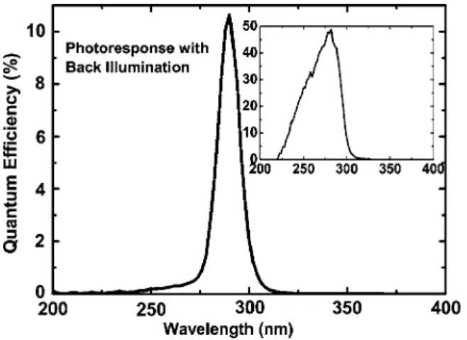
Figure2shows the quantum efficiency measurements of 150m diameter devices at 25 V. Under a 25 V reverse bias voltage, the device had a maximum quantum efficiency of 48% at 282 nm and of 10.64% at 290 nm with front and back illuminations, respectively. As can be seen in Fig.2, the devices are responsive to photons with energies higher than 4.4 eV which qualified them to be solar blind. According to the quantum efficiency data, the photocurrent does not sig-nificantly increase after 20 V. Therefore, we set the unity gain at 20 V. We also had to adjust the light source intensity for front and back illuminated photomultiplication measure-ments. We used the Schottky barrier diode to achieve pure electron injection when illuminated on the Schottky metal side with photon energy higher than the Schottky barrier height共290 nm兲 and pure hole injection when illuminated on the sapphire side with energy higher than the band gap.19
Figure 3 shows the reverse bias voltage dependence of the electron and hole multiplication factors, Mnand Mp. The multiplication factors are the ratios of the multiplied photo-currents to the primary photophoto-currents injected. The impact ionization coefficients共Fig.4兲 can be found from the
multi-plication factor data using the following formulation:20–22
共Em兲 = 2d W02 1 MnMp dMp dV + Mp Mn x
冉
␣关E共d兲兴 − 兵␣关E共d兲兴 −关E共d兲兴其 1 Mp冊
, 共1兲 ␣共Em兲 = 2d W02 1 Mn dMn dV +␣关E共d兲兴Mp−共Em兲共Mn− 1兲, 共2兲 W0=冋
2 qNd册
1/2 , 共3兲 E共x兲 =qNd 共W − x兲, 共4兲where Emis the electric field near the Schottky contact metal for a certain applied bias voltage, and E共d兲 is the electric field at the n−-n+junction. E共x兲 is the electric field at depth x
from the Schottky metal and n−layer interface, and V is the
applied bias voltage across the device. Figure4 shows the impact ionization coefficient data that were extracted from the multiplication factor data Mn and Mp. According to our calculations,␣is larger thanfor the range of electric field 0.78⬍E⬍1.88 MV/cm. The ratio of␣todecreases as the electric field increases. The impact ionization coefficients can be fitted into an exponential form,
␣共E兲 = Aeexp共− Be/E兲, 共5兲
共E兲 = Ahexp共− Bh/E兲, 共6兲
where Ae= 0.6⫻106cm−1, Be= 3.6⫻106V / cm, A
h= 3.4 ⫻106cm−1, and B
h= 7.9⫻106V / cm. The theoretical elec-tron impact ionization coefficients 共reported in Ref.13兲 are
FIG. 1. Dark current of a 40m diameter photodetector.
FIG. 2. Quantum efficiency with back illumination, in which the inset shows the results for front illumination.
FIG. 3. Mnand Mpas a function of reverse bias voltage.
FIG. 4. Electron and hole impact ionization coefficients in Al0.4Ga0.6N.
significantly lower than our experimental impact ionization coefficients. We explain this discrepancy due to the lattice defects in the AlGaN layers共which cause microplasmas兲 and the nonuniform E-field distribution which were not consid-ered in the theoretical simulations of Ref.13.
In summary, we present the MOCVD growth, fabrica-tion, and characterization of AlGaN based solar-blind APDs. The impact ionization coefficients for electrons and holes were evaluated from the photomultiplication measurements.
Over the electric field range, 0.77 MV/ cm⬍E
⬍1.88 MV/cm,␣is found to be larger than.
This work is supported by the European Union under the
projects EU-NOE-METAMORPHOSE,
EU-NOE-PHOREMOST, and TUBITAK under Projects Nos.
104E090, 105E066, and 105A005. One of the authors共E.O.兲 also acknowledges partial support from the Turkish Academy of Sciences.
1J. C. Campbell, S. Demiguel, F. Ma, A. Beck, X. Guo, S. Wang, X. Zheng,
X. Li, J. D. Beck, M. A. Kinch, A. Huntington, L. A. Coldren, J. Decobert, and N. Tscherptner, IEEE J. Quantum Electron. 10, 777共2004兲.
2K. A. McIntosh, R. J. Molnar, L. J. Mahoney, A. Lightfoot, M. W. Geis,
K. M. Molvar, I. Melngailis, R. L. Aggarwal, W. D. Goodhue, S. S. Choi, D. L. Spears, and S. Verghese, Appl. Phys. Lett. 75, 3485共1999兲.
3J. C. Carrano, D. J. H. Lambert, C. J. Eiting, C. J. Collins, T. Li, S. Wang,
B. Yang, A. L. Beck, R. D. Dupuis, and J. C. Campbell, Appl. Phys. Lett.
76, 924共2000兲.
4A. Osinsky, M. S. Shur, R. Gaska, and Q. Chen, Electron. Lett. 34, 691
共1998兲.
5S. Verghese, K. A. McIntosh, R. J. Molnar, L. J. Mahoney, R. L.
Aggarwal, M. W. Geis, K. M. Molvar, E. K. Duerr, and I. Melngailis,
IEEE Electron Device Lett. 48, 502共2001兲.
6K. A. McIntosh, R. J. Molnar, L. J. Mahoney, K. M. Molvar, N. Efremov,
and S. Verghese, Appl. Phys. Lett. 76, 3938共2000兲.
7B. Yang, T. Li, K. Heng, C. Collins, S. Wang, J. C. Carrano, R. D. Dupuis,
J. C. Campbell, M. J. Schurman, and I. T. Ferguson, IEEE J. Quantum Electron. 36, 1389共2000兲.
8J. B. Limb, D. Yoo, J. H. Ryou, W. Lee, S. C. Shen, R. D. Dupuis, M. L.
Reed, C. J. Collins, M. Wraback, D. Hanser, E. Preble, N. M. Williams, and K. Evans, Appl. Phys. Lett. 89, 011112共2006兲.
9T. Tut, Serkan Butun, Bayram Butun, Mutlu Gokkavas, HongBo Yu, and
E. Ozbay, Appl. Phys. Lett. 87, 223502共2005兲.
10R. McClintock, A. Yasan, K. Minder, P. Kung, and M. Razeghi, Appl.
Phys. Lett. 87, 241123共2005兲.
11Ismail H. Oguzman, Enrico Bellotti, Kevin F. Brennan, Jan Kolnik,
Rong-ping Wang, and P. Paul Ruden, J. Appl. Phys. 81, 7827共1997兲.
12J. C. Cao and X. L. Lei, Eur. Phys. J. B 7, 79共1999兲. 13C. Bulutay, Semicond. Sci. Technol. 17, L59共2002兲.
14K. Kunihiro, K. Kasahara, Y. Takahashi, and Y. Ohno, IEEE Electron
Device Lett. 20, 608共1999兲.
15N. Biyikli, T. Kartaloglu, O. Aytur, I. Kimukin, and E. Ozbay, Appl. Phys.
Lett. 49, 2838共2001兲.
16E. Ozbay, N. Biyikli, I. Kimukin, T. Tut, T. Kartaloglu, and O. Aytur,
IEEE J. Sel. Top. Quantum Electron. 10, 742共2004兲.
17T. Tut, N. Biyikli, I. Kimukin, T. Kartaloglu, O. Aytur, S. Unlu, and E.
Ozbay, Solid-State Electron. 49, 117共2005兲.
18S. M. Sze, Semiconductor Devices Physics and Technology共John Wiley &
Sons, New York, 1985兲, p. 78.
19M. H. Woods, W. C. Johnson, and M. A. Lampert, Solid-State Electron.
16, 381共1972兲.
20N. Tabatabaie, V. M. Robbins, N. Pan, and G. E. Stillman, Appl. Phys.
Lett. 46, 182共1985兲.
21S. L. Fu, T. P. Chin, M. C. Ho, C. W. Tu, and P. M. Asbeck, Appl. Phys.
Lett. 66, 3507共1995兲.
22B. K. Ng, J. P. David, S. A. Plimmer, M. Hopkinson, R. C. Tozer, and G.
J. Rees, Appl. Phys. Lett. 77, 4374共2000兲.