HIGHLY EFFICIENT OPTOELECTRONIC PROPERTIES OF DOUBLY DOPED SnO2 THIN FILM DEPOSITED BY SPIN COATING TECHNIQUE
A.KOCYIGITa, D. TATARb,*, A. BATTALc, M.ERTUĞRULd AND B. DUZGUNb
a Health Services Vocational High School, Igdir University, Igdir, Turkey
b K.K. Education Faculty, Department of Physics Education, Ataturk University,
Erzurum Turkey
c Education Faculty, Department of Science Education, Muş Alparslan University,
Muş, Turkey
dAtaturk University, Engineering Faculty, Department of Electricity and Electronics,
25240 Erzurum, Turkey.
In this study, we investigated structural and optical properties of doubly doped SnO2 thin films
prepared successfully by sol-gel spin coating technique on optical glass substrates. Low cost precursor SnCl2 .2H2O for host precursor and Sbcl3 and NH4F dopant source are used (for 4 %
wt. Sb and 30 % wt. F). X-ray Diffractometer, UV-Vis spectrophotometer, scanning electron microscope (SEM) and atomic force microscopy (AFM) were performed on AFTO (Antimony and Fluorine Doped SnO2) films. Structural studies reveals the presence of orthorhombic
structure with preferential orientation of (021) and (042). The dislocation density of the doubly doped film is smaller than densities mentioned in the literature for doubly doped SnO2. SEM
and AFM studies reveal the surface of AFTO to be made of nanocrystalline particles. The transmittance of the films in the visible range is 85-97 %, the best transparent film for doubly doped tin oxide films in the literature. Eg values are quite wide, 4.45 eV and better linearity
was obtained in the (αhν)2 vs. (hν) plots for E
g values. The band gap attained for the doubly
doped films in this study is higher than the values reported for doubly doped tin oxide films prepared from prophanol solution of SnCl2.2H2O precursor. Our experimental results indicated
that AFTO thin films with high optical quality could be synthesized by sol-gel spin coating techniques.
(Received November 13, 2012; Accepted November 28, 2012)
Keywords: SnO2: Sb: F thin films, Spin coating method, Optoelectronic devices, Solar cell
1. Introduction
Transparent conducting oxides are materials providing both high optical transmittance and high electrical conductivity simultaneously. Antimony and fluorine doped tin oxide (AFTO) films are an n-type semiconductors. Semiconductor materials have been extensively investigated because of their unique size dependent electronic, magnetic, optical, and electrochemical properties [1–5]. As an n-type semiconductor with a wide band gap energy, tin oxide spans a wide range of applications from conductive electrodes and transparent coatings to heterojunction solar cells and chemical sensors [6,7]. Tin oxide is a semiconductor material highly transparent and with high mechanical and chemical stability, except for their interactions with oxygen atoms at high temperature [8]. In addition to its high optical transmission due to a wide optical band gap nearly 3.8 eV, SnO2 thin films have high n-type conductivity, which is due to their non-stoichiometric character associated with oxygen vacancies and interstitial tin in the lattice [9, 10, 11].
_____________________________________ *Corresponding author: [email protected]
Many dopants, such as antimony (Sb), arsenic (As), fluorine (F), indium (In), molybdenum (Mo), and phosphorus (P) have been used to improve the electrical properties of tin oxide films [12]. Among these, Sb and F are found to be the most commonly used dopants for solar cell layers.
Tin oxide films with low resistivity can be realized by doping either Sb or F. Undoped and doped tin oxide films have been deposited by various methods [12-17]. The conventional techniques such as CVD, PVD have been widely followed [18-20] to study the effect of high dopant concentration on structural, optical and electrical properties of the doped material. The number of studies [21–23] on the sol–gel based antimony or flor doped SnO2 films have been extremely rare. The sol–gel processing exhibits good uniformity and better-controlled composition [24] for thin film deposition by the spinning method. In this study, an attempt is made to find different layers effect by simultaneously doping antimony and fluorine. Even though, Thangaraju and Ravichandran et al. have reported [13, 25, 26, 27] some properties of the doubly doped TO films, detailed report on these films are hardly available in the literature.
In the present work, antimony and fluorine doped tin oxide (AFTO) films were fabricated using SnCl2.2H2O (98 % purity, Merck), Sbcl3 (99 % purity, Merck), and NH4F (98 % purity, Sigma-Aldrich) as precursor. The aim of this work is to investigate the relationship between the multilayers and the structural and optical properties of SnO2: Sb: F thin films, deposited by spin coating technique. The results obtained have been compared with the specified results by several researchers and the reason was discussed.
2. Experimental
SnCl2.2H2O (0.05 M) 0.564 g added to prophanol and NH4F (30 % wt.), SbCl3 ( 4 % wt.) was then added as dopant source in the solvent. 10 ml HCl were then added to the solvent and completed to 50 ml. This solvent was stirred and heated 1 hour for solution phase. Solution became transparent and was then added spin coater (Laurell WS-650 series spin processor) with static method at 3000 rpm. The substrates were cleaned in washing machine using bidistilled water, and then heated in oven at 250oC for 1 h. Multilayer coatings were spun at a speed of 3000 rpm for 10 s. The layers were first dried in air then sintered in oven at 150oC for 1 h. At the end film annealed for one hour at 400 οC in tube furnace.
X-ray diffraction patterns were recorded using X-ray diffractometer (Rigaku D Max-IIIC) which was operated at 40kV and 30mA with X-ray source of CuKα radiation having wavelength 1.5406˚ A. The surface morphology of the coating was imaged using a high resolution scanning electron microscopy (SEM) and atomic force microscopy (AFM). SEM images were obtained by employing Zeiss Evo-LS-10 model scanning electron microscope and AFM, which was produced by nanomagnetics instrument. Perkin Elmer UV–Vis-NIR double beam spectrophotometer (Lambda-35) is used to record the transmission spectra in the range of 300–1100nm.
3. Result and discussion 3.1.Structural properties
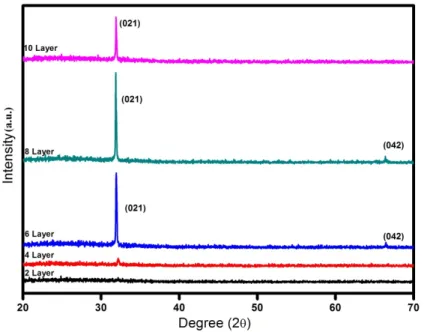
X-Ray Diffraction (XRD) patterns of doubly doped SnO2 (SnO2: Sb: F) thin films depict that films are crystalline in nature. XRD patterns reveal that films are not good crystalline for low layers but high layers are good crystalline. XRD graph showed that films have grown orthorhombic structure with the (021) and (042) preferential orientation (ICDD Card No: 78-1063). No other peaks have emerged. The obtained graph is rather original, because the films are single crystalline and have not been found in the literature. A similar conclusion has been given by Radheshyam Rai et al. for SnCuO3 [28]. The high intensity of the peak suggests that these thin films mainly consist of the crystalline phase. As the number of layers is increased, the crystallinity of the thin films is enhanced as manifested by the intensity and sharpness of the XRD peaks of the AFTO thin films as shown in Fig. 1. The crystallinity increases with increasing layer number because of amount of tin oxide in the surface of the films. Lower layers (2 and 4) don’t exhibit well crystalline in nature.
Fig. 1: XRD patterns of doubly doped thin film for different layers
The quantitative improvement in the crystallinity can be understood from the calculation of the grain size. The grain size D is determined from the full width half maximum (FWHM) value of the dominant (021) reflection, using Scherrer’s formula [29]: D = 0.9 λ/(β cosθ) where λ is the x-ray wavelength (1,5406 Å for CuKα), θ is the diffraction angle and β is the FWHM. The calculated values are tabulated in Table 1. It is seen that the grain size decreased with increasing layers number and reached minimum at 6 layers then increased with the increasing deposition layer. AFTO nanoparticle size sharply decreases from 222.31 nm (at room temperature) to smaller than 58.7 nm at size layers. It finally slowly increases to 72.6 nm at higher layers. It is explained that amount of tin oxide in the surface of the films increases with increasing deposition and decreases grain size. Different researcher find changes the grain size for annealing temperature. They generally said that grain size increases with increasing annealing temperature [30, 31, 32]. In this study deposition layer effect investigated and found that grain sizes nearly decreases with increasing deposition layer.
The dislocation density (δ), defined as the length of dislocation lines per unit volume, has been estimated using the equation, δ=1/D2 [33]. Since δ is the measure of the amount of defects in a crystal, the small values of δ obtained in the present study confirmed the good crystallinity of the doubly doped TO films deposited by spin coating. These conclusions also were given Table 1.
Table 1. Structural parameters table of different layer deposition of doubly doped tin oxide Layer Numbers 2θ (Degree) FWHM D(nm) δx10
18 (lines/m2) RMS(nm) 2 32,18 0,042 222,31 0,066 230,15 4 32,14 0,054 174,07 0,108 172,14 6 31,94 0,161 58,02 0,976 156,91 8 31,88 0,134 69,71 0,677 174,81 10 31,90 0,129 72,67 0,623 255,86
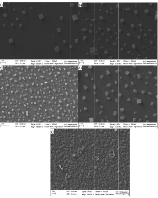
2θ- The Diffraction Angle; FWHM- Full width half maximum; D-Grain size; δ-Dislocation density The surface morphologies of the SnO2: Sb: F thin films, was also investigated by using Scanning electron microscope (SEM) and atomic force microscopy (AFM). Scanning electron microscope (SEM) images were given in Fig. 2 for different layers. These images revealed that films
are unifo data. It h has also grain siz SEM im is attribu have not T with dif (from 2 of SnO2: increase grains is found to 6 layers
form and hom has been ob been observ ze decreases. mages. It is ob uted to the or t been observ The atomic f fferent depos layers to 10 :Sb:F films a in layer nu s uniform on o be 156.91 to is the lowest mogenous. T served that i ved that nan . Good cryst bserved that rthorhombic ved in the lite
Fig. 2: SEM a force micros sited layers. 0 layers) dop as a function umber. The g the substrate o 255.86 nm t in comparis These observ increasing de noparticles of tallinity of th there are cub structure of erature for tin
EM micrograph a) 2, b) 4, c) 6, scopy surface Fig. 3(a)-(e ped SnO2 film
of the layer grains can b e surface. Th m doubly dope
son with oth
vations stron eposition lay f the films i he films obta be and pyram f SnO2 and S in oxide film hs of doubly d 6, d) 8, e) 10 la e 3D images e) show 3D ms and Fig. number. Th e seen almo he root mean ed film. The her films (Tab
ngly support yer increases increase with ained for hig mid shaped n SnO in the gi ms.
doped tin oxid ayers depositi s were obtain
atomic forc 3(f) showed he number of
ost all over t n square (RM root mean s ble 1). As th t the results s homogenei h increasing gh number o nanostructure iven literatur de thin films on
ned for SnO2 ce microscop d the surface f smaller grai the substrate MS) values of quare roughn e layer numb obtained fro ity and unifo layer depos f layer could es in the surf re [34]. Thes 2:Sb:F films py images o roughness v ins increased e. The distrib f surface rou ness of the fi bers increase om XRD ormity. It sition and d be seen face. This se images prepared of doubly variations d with the bution of ughness is films with ed from 1
to 6, the roughness of the films decreased from 230.15 to 156.91 nm, then increased to 255.86 nm. The AFM microphotographs of the SnO2:Sb:Ffilms were also shown that the grain size of the films decreased with the increase in the layer numbers. Detailed atomic force microscopy study revealed that the roughness of the film was dependent on the layer numbers.
Fig. 3: Fig. 3. AFM surface 3D images of doubly doped films as a function of layer number: (a) 2, (b) 4, (c) 6, (d) 8, (e) 10, (f) the surface RMS roughness variation of doubly doped films as a function of layer number
(a) (b) (e) (f) (c) (d)
3.2. Optical properties
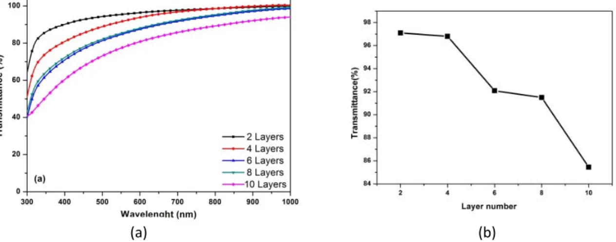
The optical properties of AFTO coating were characterized by measuring the optical transmittance (T) spectrum in the range 300–1100 nm (Fig.4(a)). The layers were deposited at spinning speed of 3000 rpm for 10 s. The thickness of the layers is supposed to increase linearly by increasing the number of deposited layers but the optical properties (transmittance) was found to decrease (Fig.4(b)). The information of optical transmittance is important in evaluating the optical performance of semiconducting oxide thin films. From the spectra it is observed that the transmittance in the visible range is 85-97 % for the doubly doped TO films grown by spin coating technique at different layer deposition. Although it is quite difficult to deposit doubly doped tin oxide films with this method, we successfully deposited and obtained quite homogeneous and transparent films in the literature. The transmittance measurements indicated that present AFTO thin films can be used as a window material for solar cell application due to their best transmittance of films is around 95%. The value obtained for AFTO films is the highest value compared to other studies that use other methods.
Fig. 4: (a) Optical transmission spectra of doubly doped tin oxide thin films for different layer deposition (b) The optical transmittance values doubly doped films as a function of layer number
The absorption coefficient (α) can be calculated from the transmittance (T) values at the absorption edge from the Lambert’s law α = ln (1/T)/t [35]. The variation of absorption coefficient against photon energy (hν) has the form of α = A (hν - Eg)n/2, where E
g is the band gap, A is a constant related to the effective masses associated with the bands and n is a constant which is equal to one for a direct-gap material and four for an indirect-gap material [35].
Table 2. Transmittance and Band gap energy values for different layer deposition Layer Numbers T (%) (λ~700 nm) Eg (eV)
2 97,10 4,25 4 96,80 4,25 6 92,08 4,45 8 91,50 4,41 10 85,45 4,25
T- the transmittance at 700 nm; Eg-Energy band gap (b) (a)
To determine whether the doubly doped TO films deposited using spin coating method have direct or indirect band gap, (αhν)2 vs. (hν) and (αhν)1/2 vs. (hν) plots were drawn. Since better linearity was obtained in the (αhν)2 vs. (hν) plots, the direct band gap values were determined by extrapolating the linear portion of these plots to the energy axis. The optical band gap values are also estimated using the dT/ dλ vs λ plots. The average optical transmittance and the estimated Eg values are summarized in Table 2. Eg values did not chang for different layer deposition, as can be seen better in Figure 5. But it was found that the value obtained for the films deposited with 6 layers doubly doped tin oxide is the highest value obtained in the present study (4.45 eV).
Fig. 5: Band gap graphs of doubly doped tin oxide films for different layer deposition 4. Conclusion
Doubly doped SnO2 thin films were successfully prepared by sol-gel spin coating techniques. Films were deposited on optical glass and annealed at 400oC. The microstructural and optical properties of AFTO thin films were investigated different layer number in the layer range from 2 to 10. Optical properties as well as the structure and morphology of the films were found to depend on the multilayer. XRD patterns revealed that films are single crystal in nature and have preferential orientation (021) and (042) plane. X-ray diffraction results also confirmed that the various AFTO thin films consisted of nanoparticles with average grain size in the range of 222 -58 nm. SEM and AFM images depict that films are homogenous and uniform. The microstructure analysis of the AFTO thin films demonstrated that the layer deposition is a very important parameter. It affects crystalline microstructure and optical properties of the thin films. The highest transmittance of around 95% at 700 nm has been observed. The transmittance measurements indicated that present AFTO thin films can be used as a window material for solar cell devices due to their best transmittance is around 95 %. Various optical parameters such as optical band gap energy were calculated from the optical transmittance data recorded in the wavelength in the range of 300-1100 nm. We found that the optical band gap energy of AFTO thin films is the widest band gap values in the literature with this method. Wide optical band gap (4.45eV) and reasonable visible transmittance (95%) make these doubly doped films desirable candidates for low-cost solar cell materials. These findings revealed that doubly doped SnO2 thin film layer deposition up to 6 is a good window material for solar cell devices. This point will be studied in the immediate future. Our experimental results indicated that SnO2 thin films with the high optical quality could be synthesized by sol-gel spin coating techniques.
Although further research is necessary, the AFTO films show a promising potential for the improvement of AFTO thin film applications.
Acknowledgements
The authors sincerely thanks to Erzurum Ataturk University Scientific Research Projects (B.A.P. 2011/218) Centre Turkey for financial support.
References
[1] A.P. Alivisatos, Science 271, 933 (1996).
[2] C.B. Murray, D.J. Norris, M.G. Bawendi, J. Am. Chem. Soc. 115, 8706 (1993). [3] M. Nirmal, L. Brus, Acc. Chem. Res. 32, 407 (1999).
[4]G. Turgut, D. Tatar and B. Düzgün, Asian Journal of Chemistry 25, 245 (2013). [5] D. Tatar, B. Düzgün, Pramana – J. Phys., 79, 137 (2012).
[6] Y.S. He, J.C. Campbell, R.C. Murphy, M.F. Arendt, J.S. Swinnea, J. Mater. Res. 8, 3131 (1993). [7] J. Watson, Sens. Actuators 5, 29 (1984).
[8] H. Pink, L. Treitinger, L. Vite, Jpn. J. Appl. Phys. 19, 513 (1980). [9] Z.M. Jarzebski, J.P. Marton, J. Electrochem. Soc. 123, 199 (1976).
[10] D. Y. Torres Martınez, R. Castanedo Perez, G. Torres Delgado, O. Zelaya Angel, J Mater Sci: Mater Electron 22, 684 (2011).
[11] D. Tatar, G. Turgut and B. Düzgün, Romanian journal of physics, accepted papers (in pres). [12] H. Kim, R.C.Y. Auyeung, A. Pique, Thin Solid Films 516, 5052 (2008).
[13] B. Thangaraju, Thin solid films 402, 71 (2002).
[14] H.L. Ma, D.H. Zhang, S.Z. Win, S.Y. Li, Y.P. Chen, Sol. Energy Mater. Sol. Cells 40, 371 (1996).
[15] H. Kim, A. Pique, Appl. Phys. Lett. 84, 218 (2004).
[16] M.H. Madhusudhan Reddy, A.N. Chandorkar, Thin Solid Films 349, 260 (1999).
[17]G. Turgut,D. Tatar, B. Düzgün, EÜFBED- Erzincan Üniversity Graduate School of Natural and Applied Sciences Journal 5, 13 (2012).
[18] Srinvasa Murty N, Jawalekar SR. Thin Solid Films 108, 277 (1983). [19] Kim KS, Yoon SY, Lee WJ, Kim KH. Surf Coat Technol 138, 229 (2001).
[20] K.O. Grosse-Holz, J.P.M. Cillessen, M.W.J. Prins, P.W.M. Blom, R.M. Wolf, R. Waser, Materials research society symposium proceedings, Physics of organic semiconductors 401, 67 (1995). [21] C. Terrier, J.P. Chatelon, R. Berjoan, J.A. Roger, Thin Solid Films 263, 37 (1995).
[22] C. Terrier, J.P. Chatelon, J.A. Roger, Thin Solid Films 295, 95 (1997).
[23] A.P. Rizzato, C.V. Santilli, S.H. Pulcinelli, A.F. Craievich, J Appl. Crystallogr 36, 736 (2003). [24] T.D. Senguttuvan, L.K. Malhotra, Thin Solid Films 289, 22 (1996).
[25] K. Ravichandran, G. Muruganantham, B. Sakthivel, P. Philominathan, Journal Of Ovonıc Research, 5, 63 (2009).
[26] K. Ravichandran, G. Muruganantham K Saravanakumar S Karnan B Kannan, R Chandramohan, B Sakthivel, Surface Eng 25, 81 (2009).
[27] K. Ravichandran, G. Muruganantham, Sakthivel, B. Physica-B Con. Mater., 404, 4299 (2009). [28] T.D. Radheshyam Rai, S.T Senguttuvan,. Lakshmikumar, Computational Materials Science 37, 15 (2006).
[29] L.N. Patro, K. Hariharan, Materials Letters 80, 26 (2012).
[30] V. Arıvazhagan, S. Rajesh, Journal of Ovonic Research, 6, 221 (2010).
[31] S. Bazargan, N. F. Heinig, D. Pradhan, and K. T. Leung, Crystal Growth & Design, 11, 247 (2011).
[32] X. Zhong, B. Yang, X. Zhang, J. Jia, G. Yia, Particuology 10, 365 (2012).
[33] V. Senthilkumar, P. Vickraman, J.J. Prince, M. Jayachandran, C. Sanjeeviraja, Philosophical Magazine Letters, 90, 337 (2010).
[34] S. Das, S. Chaudhuri, S. Maji, J. Phys. Chem. C, 112, 6213 (2008). [35] E. Elangovan, K. Ramamurthi, Appl. Surf. Sci. 249, 183 (2005).