complex passive integrated optical circuits of
arbitrary rectilinear topology
GUrkan Onal
Ayhan Altinta, MEMBER SPIE Haldun M. Ozaktas
Bilkent University
Department of Electrical and Electronics Engineering
06533 Bilkent Ankara, Turkey
E-mail: [email protected]
1 Introduction
Ithas been widely argued that the use of optical intercon-nections may provide several benefits over electrical inter-connections in many situations.'7 Comparisons of perfor-mance characteristics—such as speed, bandwidth, power consumption, and footprint area—of electrical and optical or optoelectronic circuits have been published.8'2 Some par-ticular examples of practical implementations of optical in-terconnections are a multifiber bus for module-to-module connections, a mastercard for a backplane, waveguide arrays for multichip modules, and a chip-level clock distribution demonstrator for chip-level optical
Single-mode channel waveguides can be made the basis of an integrated optics approach to providing optical
inter-connections (Ref. 14, p. 59). Materials such as silicon
nitride'5 or various polymers'6"7 can be used to realize the passive waveguides. Waveguide interconnects between chips on a multichip module, between individual chips or multichip modules on a printed circuit board, and between boards at-tached to a backplane have previously been Corn-mercial simulation tools for analyzing channel waveguides have already been developed that are mostly based on the beam propagation method'9'20
Despite these and similar efforts, we are not aware of any general approach toward the analysis and design of complex integrated optical circuits of an arbitrary circuit diagram con-taining many paths and segments. Systems for analyzing and simulating electrical integrated circuits are many and well developed, as are computer-aided design systems for very large scale integration (VLSI) systems. An abstraction of design considerations has led to so-called design rules, such as the one stating that two parallel metal lines must be sep-Paper OIP-03 received May 28, 1993; revised manuscript received Dec. 15, 1993; accepted for publication Jan. 21, 1994.
1994 Society of Photo-Optical Instrumentation Engineers. 009 l-3286/94/$6.00.
Abstract. Optical interconnections can be beneficially employed at the chip-to-chip or backplane level of high-performance computing systems. One method of providing high speed and density interconnections among a large number of integrated circuit chips is with a passive inte-grated optics circuit. We have developed a method of breaking down arbitrarily complex rectilinear circuits into elementary blocks whose loss and coupling properties are known. Thus, the overall loss and noise for each connection can be calculated. A high-speed algorithm based on this method has been implemented. The high speed of our analysis sys-tem makes it suitable for incorporation in an iterative design syssys-tem, which determines the minimum spacings between the guides and results
in acceptable crosstalk and noise levels.
aratedby a distance of at least 3X, where X corresponds to the smallest feature size of that technology (Ref. 21, p. 48). The purpose of this study is to develop computer-aided analysis and design systems, together with similar abstrac-tions as mentioned earlier. These, it is hoped, will make the realization of complex optical circuits possible.22 In this pa-per, we will be concerned with analysis and simulation only, and will briefly mention how this analysis system can be made the basis of a design system. More concretely, we will report on a system that can calculate the loss and crosstalk for passive, single-mode, fairly complex channel waveguide circuits.
In the system developed, the signal and noise (undesired signal) levels of any point in the circuit are determined, given the topology of the circuit and the initial signal and noise levels at the inputs. The characteristic parameters ofthe wave-guides, such as their propagation, attenuation, and coupling constants are also specified as inputs. The algorithm is very fast, so that adjustments can be made to improve the signal, noise, and crosstalk levels and the calculations repeated sev-eral times until a satisfactory signal-to-noise ratio (SNR) is achieved in all interconnects. Thus, it is a short step from our analysis/simulation system to the realization of a design system.
In Sec. 2,theproblem is stated and the method of analysis is described. In Sec. 3, mathematical expressions for signal
and noise calculations for different kinds of basic circuit features are given. The fast algorithms we developed are explained in Sec. 4. An example circuit with 15 paths is
analyzed and the results are given in Sec. 5. The use of our method and possible further improvements are discussed in
2 Problem
Description and ApproachWeanalyze planar integrated optical circuits constructed of single-mode waveguides of arbitrary topology and
complex-Subject terms: optical interconnects and packaging; integrated optics. OpticalEngineering 33(5), 1596—1603 (May 1994).
Sec. 6.
1596 / OPTICAL ENGINEERING / May 1994 / Vol. 33 No. 5
Downloaded from SPIE Digital Library on 20 Oct 2010 to 66.165.46.178. Terms of Use: http://spiedl.org/terms
Downloaded From: https://www.spiedigitallibrary.org/journals/Optical-Engineering on 1/28/2019 Terms of Use: https://www.spiedigitallibrary.org/terms-of-use
ity, subject to the restrictions discussed later. Given the input signal and noise levels, we determine the output signal and noise levels. It is assumed that the circuits to be analyzed are
rectilinear, so that the interconnects can be mapped on a
Cartesian grid. We also assume that the interconnections are one-to-one; fan-out and fan-in are not allowed. Allowing such interconnections requires substantial modification of the de-veloped procedures and algorithms, so that removal of this restriction is postponed for future research.
We assume that all of the waveguides are of the same
width, geometry, and refractive index profile. The input is
most likely a light source, and the output is most likely a light detector, both of which are probably situated on, or
attached to, electronic integrated circuit chips. We do not make any assumptions regarding the nature of these
trans-ducers; any imperfect coupling into or out of the optical
circuit is lumped into the efficiency factors and loutpur The light propagating in a waveguide is affected by bends, junctions, and neighboring guides. To calculate these effects
as we go along a particular interconnection, we mentally
divide the waveguide into what we call segments, which are elementary features of an interconnection. For coupling, only nearest neighbor waveguides are taken into consideration. This does not mean, however, that we totally disregard farther neighbor effects; the effect of a second-nearest neighbor is accounted for indirectly (since an undesired signal compo-nent coupled from the second-nearest to the nearest neighbor will have an effect on the total signal coupled into the wave-guide under consideration, via the coupling from the nearest
neighbor). Although this process is not exact, taking into
account the coupling between each and every pair of circuit segments does not present itself as a formidable alternative, from both an analytical as well as a computational perspec-tive. In any event, if a circuit is going to work properly, the overall coupling between paths must not exceed a small frac-tion of the signal level. This requirement means that for such a circuit, higher order coupling would usually be a much
smaller fraction of the signal.
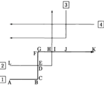
Segmentation is discussed further in Sec. 4. 1 .However, the simple circuit shown in Fig. 1 can help us understand the main idea. Each letter indicates a point where we break the interconnect into segments, thus we can refer to segments by letter pairs, such as CD. Some segments have a length, such as CD, JK. Others do not, such as BC, DE. The signal and noise levels associated with a segment are those at the ending point of it, thus the signal level of segment CD is the signal level at point D, 5D' andthe noise level of the same segment is the noise level at the same point, nD .Thesignal and noise levels correspond to the field amplitudes. As we propagate
along a particular path, the signal level decreases due to
attenuation and coupling losses. On the other hand, the noise level increases due to coupling from other paths. The signal and noise at a segment depend on those at the previous seg-ment and those at the segseg-ments of the nearest neighboring waveguides. For example, the signal and noise levels at point B in Fig. 1 depend on the signal and noise levels at points A and L. Each path in the circuit is segmented individually, that is, segmentation is path dependent. During segmentation of a path, intersections and bends are noted, and the structure around the path is searched to find the nearest parallel
wave-guides on both sides. Any change in the structure of the
neighboring guides indicates that the present segment has
ended and a new segment should be created afterward. Hence, in a single segment, the neighboring waveguides, that is, the closest parallel guides, do not change their structure.
Segments are created with the purpose of isolating circuit features that are easily analyzed. As illustrated by our ex-ample, any circuit satisfying the previously mentioned as-sumptions can be broken down into five circuit features, that is, basic elements of the circuit, namely,
1. stretch of waveguide with no neighbors
2. stretch of waveguide with a neighbor on one side 3. stretch of waveguide with neighbors on both sides 4. orthogonal bend of a waveguide
5. orthogonal intersection of two waveguides.
For each interconnect, we start with a given signal and noise level at the input. Since the effect of each of the preceding circuit features is known, we can calculate the loss in signal power and the accumulation of undesired crosstalk by the time we reach the output. We work with two field amplitudes, one denoting signal level and one denoting noise. (Noise is defined so as to include all undesired coupling into the guide. If a detector is tied to the output, the thermal and shot noises associated with it must be added to the figure our system produces.)
Since we cannot expect that there will be a predetermined or fixed phase relationship between the various light sources, we assume that the phase relationships between the inter-acting signals are such so as to result in the greatest increase in noise and the greatest decrease in signal level. This type of worst-case analysis is necessary because the phases of the light sources may drift over time.
If the noise and signal levels of all neighboring intercon-nects were known to start with, one could calculate the signal and noise level at the output of a particular interconnect by working one's way along each segment, from the light source to the detector (i.e., from point A to point K in Fig. 1). How-ever, to begin with, we do not have the signal and noise levels at any interconnect. Thus, a system of equations relating all of the signal and noise levels must be created and solved to obtain the desired output signal and noise levels:
x=Tx+1,
(1)where x is the vector whose elements are the signal and noise levels for all the segments, Iisthe matrix relating the signal and noise at any segment to those at previous segments and
Fig. 1 Example circuit illustrating the process of segmentation.
(Path numbers are labeled at the inputs. Arrows indicate the out-puts.)
neighbors as explained in the next section, and 1isthe vector of input sources.
3
Signal and Noise Level Calculations for theFive Basic Circuit Features
Foreach interconnection path, starting from the source up to the detector, each segment can be modeled as one of the five elementary features mentioned in the previous section. The signal and noise calculations for these five circuit features are described next.
3.1 Stretch of a Single Waveguide
Theattenuation is assumed to be uniform along a waveguide. Both signal and noise components are attenuated by a factor
of e c 1,where c is the attenuation coefficient and 1 is the
length of this segment of the guide. The following can be
given as an example of the attenuation coefficient for Ti:LiNbO3. The loss is 1 dB/cm at ).= 0.633rim, 0.5 dB/cm
at X=1.15 xm, and 0.2 dB/cm at X=l.52pm
(Ref. 23, p. 224)
3.2 Stretch of Two Parallel Waveguides
Nowwe consider that on one side of the waveguide in con-sideration there is a parallel running waveguide.
In such a structure, if s1 and n1 are the signal and noise levels of the first guide at the input side of the segment, s2 and n2 are those of the second guide, / is the length of the parallel run along this segment, a is the attenuation coefficient along a waveguide, and K is the coupling coefficient between the waveguides, then the signal and noise levels of the first
guide at the output are given by the following equations (Ref. 24, p. 626):
s =slcos(Kl)e1
The e a
1term is related to attenuation. The cosine term
accounts for the fact that part of the signal is out-coupled to the other guide. The sine term accounts for the fact that the signal and noise propagating in the other guide is coupled into the first guide. This undesired coupling accumulates as noise. As mentioned before, we are assuming the worst pos-sible phase relation between the light propagating in both guides.
We must mention an approximation inherent in this method of analysis. As illustrated in Fig. 2, light propagating inside guide 1 interacts with light propagating in both the horizontal and the vertical portions of guide 2. The effect of interaction with the vertical portion is somewhat analogous to the fringing effect in a parallel plate capacitor. As long as the distance of parallel interaction is long, the fringe effect can be neglected with small error. (If the distance of parallel
interaction is small, this would mean that the overall coupling over this segment of the interconnect is small compared to other segments, so that again the error is small.)
3.3 Stretch of Three Parallel Waveguides
Generally, a straight running waveguide, unobstructed by bends or intersections, will have neighboring waveguides on both sides. Most segments will be of this type.
In a structure of three parallel waveguides, if s1, s3 and
1 '
3
are the signal and noise levels of the outer guides at the input, respectively, s2 and n2 are those of the center guide, / is the length of the waveguides, and a is the attenuation coefficient along a waveguide, the signal and noise levels ofthe center guide at the output are given by the following expressions (Refs. 25, pp. 136—137, and 26):
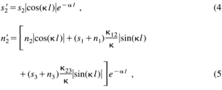
s=s2cos(K/)e' ,
(4)n =
[n2cos(Kl) + (s1 + n1)sin(K/)K23 1
+(s3+n3)—s1n(K/)
le '
, (5)K
where K= (K2 +K3)/2, K1i5the coupling coefficient
be-tween waveguide i and waveguide j,
where (i,j ) ={( 1,2),(2,3)}.
3.4 Orthogonal Bend
Inmost cases, each interconnection will suffer from at least one 90-deg bend. Smooth curved bends take up too much space, requiring as much as a 1-cm radius in weakly guiding waveguides in Ti:LiNbO3. Obviously, this limits the packing density considerably. For this reason, for right or left turns, total internal reflection mirrors, as in Fig. 3, are assumed. Due to the large index difference between core and air at the corner, the reflection coefficient is very close to unity (Ref. 23, p. 229). Such a bend can be characterized by an efficiency factor lb 'whichaccounts for the power loss as a result of the bend. Therefore, if the signal and noise levels before an
orthogonal bend are and ,
respectively,then those after the bend, s1' and n, respectively, are given by(6) (7)
3.5 Orthogonal Intersection
Unlessmultilayer optical circuits can be realized, intersection of waveguides will be unavoidable. The loss and crosstalk is very angle sensitive and the loss is minimal for normal
1598/ OPTICAL ENGINEERING / May 1994 / Vol. 33 No. 5 (2) (3)
Fig. 2 The fringing effect from the second guide to the first one is neglected.
n
n
Fig. 3 Orthogonal bend implemented by total internal reflection.
Downloaded from SPIE Digital Library on 20 Oct 2010 to 66.165.46.178. Terms of Use: http://spiedl.org/terms
Downloaded From: https://www.spiedigitallibrary.org/journals/Optical-Engineering on 1/28/2019 Terms of Use: https://www.spiedigitallibrary.org/terms-of-use
intersection, which is the only kind possible for rectilinear circuits anyway. This feature can be characterized by two parameters, one accounting for the insertion loss ('iii)andthe
other for crosstalk Thus, the signal and noise levels in the horizontal waveguide in Fig. 4 can be calculated by using the following equations:
s'=\/s ,
(8)nç=\An1+\/(s2+n2)
4 Computer Analysis and Simulation
In this section, we describe the algorithm and computer im-plementation of the analysis described earlier. Although the process of segmentation and calculation of crosstalk and cou-pling is easy to grasp intuitively, development of the appro-priate data structures and procedures that result in a fast anal-ysis system is not straightforward. Only a brief description of the algorithm and implementation is given here; details are documented in Ref. 27.
The circuit topology is represented in the form of three different data structures. The information stored in these data structures is partially redundant, however, each is structured in a particular way so as to be efficiently accessed by the
various search procedures in the algorithm. They are all
arrays-of-pointers type data structures and store the circuit topology in the following manner:
1 . Inthe first one, each pointer in the array represents a
path and each cell of the pointer corresponds to an
orthogonal bend along this path. For example, for the
circuit shown in Fig. 1 the first pointer of the array
contains the information about the first path in the cir-cuit (see Fig. 5). The first cell of the pointer maintains the coordinates of point A (A is the abscissa of point A and A is the ordinate of the same point in Fig. 5), which isthe input of the path. In the same manner, the second cell is for the coordinates of point B, the third cell is for those of point F, and the last cell is for point K, which is the output. A total of four cells exists in the pointer and they are in the correct order from the input to the output.
2. Each element of the second array corresponds to a
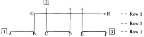
horizontal line, that is, a row, in the Cartesian grid in which the circuit is embedded. Each cell of a pointer is a horizontal line segment between two consecutive corners of a path lying on the corresponding row. The cells of the pointers are sequenced with respect to the abscissa of the left starting point of the horizontal line segment. The first pointer of the array represents the lowest horizontal line of the rectilinear Cartesian plane (9) containingthe circuit. In the circuit shown in Fig. 6, let us assume that the inputs of the first and third paths are located on row 1 .Thenthe first pointer of the array represents all the horizontal line segments lying on this row (see Fig. 7). The first cell contains the information about the first line segment AB on this row, namely the abscissa ofpoints A and B (A and B, respectively) and the path number to which these segments belong (which is 1). The second cell contains the abscissa of points C and D (
C
and D, respectively) and the path number (which is 2). The third cell contains the ab-scissa of points E and F and the path number (which is 3). There are in total three cells in the pointer and they are in the correct order from left to right. Thereis no interconnect in the second row of the circuit
shown in Fig. 6, therefore, the pointer corresponding to the second element of the array is simply a nil pointer (see Fig. 7). In the circuit, there is only one horizontal interconnect in the third row, thus, the pointer belong-ing to the third element of the array has only one cell. The rest of the array is created in the same manner. 3. The third array is very similar to the second array but
stores the vertical line segments instead of horizontal ones.
4.1 Segmentation Algorithm
The segmentation of each interconnect path is the most im-portant part of the program. A segment is defined as a part of an interconnect path that forms one of the basic circuit
L1
1—'• —'1'
Fig.4 An orthogonal intersection. Arrows represent direction of light.
H Row3 Row2
E1A
B C
D E
FE1 RowlFig.6 Example circuit illustrating the creation of array-of-pointers type data structures. (Path numbers are labeled at the inputs. Arrows indicate the outputs.)
Fig. 5 First array-of-pointers type data structure for the circuit in Fig. 1.
LIJ-Fig. 7 Second array-of-pointers type data structure for the circuit in Fig. 6; N is the total number of rows in the rectilinear plane in which the circuit is embedded.
features described in Sec. 3 (see also Fig. 1). The signal and noise levels at any segment of a path depend on those at the previous segment of the same path and those at neighboring interconnects.
The segmentation algorithm starts from the source at the first path and continues toward the detector ofthis path. When segmentation of the first path is finished, the algorithm con-tinues with the second path, third path, etc. At the end of the algorithm, the path number, orientation, signal flow direction, coordinates, distances to neighbors, and signal flow directions of the neighbors for each segment are stored.
The algorithm starts by storing the source and corner
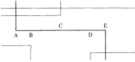
points of each path, which are conveniently available in the first array of pointers, shown in Fig. 5.Thisprocess cone-sponds to the first step in segmentation. The portion of a path running between two corners must be further segmented de-pending on neighboring parallel paths. (For instance, the por-tion AE in Fig. 8 will be further segmented into AB, BC, CD, and DE.) This is accomplished by using the following algorithm.
Again we refer to Fig. 8 as an example. In the second
anay of pointers, shown in Fig. 7, the rows just above and just below the one containing the portion (AE) of the path to be segmented, that is, the previous element in the anay, is searched for a line segment whose x coordinates may over-lap with those of the path to be segmented. If such a line
segment exists, the x coordinates describing the extent of overlap and the distance between the two lines are stored in a single cell of a newly created pointer-type data structure. In the figure, an overlap extending over the portion AB is detected. In this case, parallel runs exist both above and below the segment AB, so that this part of the path is treated as a stretch of waveguide with neighbors on both sides. We now continue working on the remaining portion BE.
The algorithm continues searching for possible overlaps in the neighboring rows of the anay of pointers of Fig. 7 and comes across the parallel run just above BC. This time, on the lower side, we do not come across a parallel run within a preset distance, so that the segment BC is designated as a stretch of waveguide with a neighbor on one side only. Then, the algorithm continues searching farther and farther rows in the data structure of Fig. 7, until it comes across the parallel run above CD, which is also treated as a single neighbor run. Finally, DE is recognized as a segment due to the parallel run on both sides. Thus, AE has been broken down into the four segments AB, BC, CD, and DE. In some cases, unlike in this example, the segments may not be recognized in the conect order (for instance, DE may be recognized before CD). Nevertheless, they are stored in the proper order by the algorithm. Then, the information conesponding to these seg-ments, in the conect order, is inserted in between the
infor-C
A B
B EFig. 8 Segmentation algorithm for a line segment AE after the
neighbors are determined in both directions.
mation conesponding to the corners A and E, which were already recognized as segments. Then, the algorithm contin-ues with segmentation of line portions between other bends
and intersections of the path. In the end, the information
pertaining to the segments is stored in the correct order, as we come across them along the path.
4.2 Self-consistent Solution of the Signal and Noise Levels
Afterall the interconnect paths are segmented, the x and 1 vectorsand the T matrix of Eq. (1) can be created. The ele-ments of the vector x are the signal and noise values asso-ciated with the segments. This vector is the unknown vector to be solved in Eq. (1). Vector 1containsthe signal and noise values ofthe input sources. Matrix T contains the coefficients relating the signal or noise values of a segment to those of the previous segments on the same path, and of segments of neighboring paths.
All the information necessary to calculate the coefficients of the matrix T can be obtained from the results of the seg-mentation algorithm (see Sec. 4.1), which contains the co-ordinates, separations, etc. of the segments, all properly la-beled and ordered. For instance, if a segment involves parallel waveguides in both directions, we use the formula given in Sec. 3 to obtain the related coefficient of the matrix T, in terms of the length and separation of the parallel run.
Then, the signal and noise values for every segment in the circuit are computed by
x=(I—T'1
(10)where Iisthe identity matrix. At most, two neighboring paths are coupled to the segment under consideration, therefore,
the matrix I —
T
has at most six nonzero elements in any row. Thus, very fast solution ofEq. (10) is possibleby using sparse matrix algorithms.It should be emphasized that the method of analysis and simulation discussed until now is independent of how the
attenuation, propagation, and coupling parameters of the
waveguides are calculated. These should be considered sim-ply as inputs to our system. The exact profile or refractive index distribution are not relevant for our programs; their effect is summarized in the mentioned parameters. Such pa-rameters may be numerically calculated28 or even experi-mentally determined. An analytic approach for calculation of these parameters for step index channel waveguides and the extension to waveguides of arbitrary profile are given in Refs. 27, 29, and 30.
4.3 Computer Implementation
Thedescribed algorithm has been implemented on a personal computer with the PASCAL programming language, with the exception of the sparse matrix solver, which was written in the C language. In this implementation, the user enters the circuit to be analyzed by means of a cursor-driven interface. The spacing of the Cartesian grid is specified by the user. While the circuit topology is being entered, the three different data structures described in Sec. 4 are created simultaneously. The user also inputs the attenuation coefficient, coupling coefficient, and the similar parameters for bends and inter-sections, and also the wavelength of light. Once these pa-rameters are entered, the signal and noise levels at any point 1600/ OPTICAL ENGINEERING / May 1994 / Vol. 33 No. 5
Downloaded from SPIE Digital Library on 20 Oct 2010 to 66.165.46.178. Terms of Use: http://spiedl.org/terms
Downloaded From: https://www.spiedigitallibrary.org/journals/Optical-Engineering on 1/28/2019 Terms of Use: https://www.spiedigitallibrary.org/terms-of-use
in the circuit can be determined in terms of the signal and noise levels at the sources. The program run is of the order of a few seconds for the circuit in Fig. 9.
An auxiliary program has also been developed that can calculate the coupling and other parameters in terms of the physical parameters of the waveguides, such as its dimen-sions, refractive indices, etc. ,forchannel waveguides. In the program, the efficiency factor and insertion loss dis-cussed in Secs. 3.4 and 3.5, respectively, are approximated by the percentage of power propagating in the core (q) as calculated in Ref. 28, p. 243. For arbitrary waveguide pro-files, the values of and q can be replaced by -q of Ref. 28, p. 257. Thus, the user has a choice of entering the circuit parameters or the physical waveguide parameters.
5 Examples and Results
For the purpose of illustration we present results for the circuit shown in Fig. 9 with 15 paths. This particular circuit turned out to have 320 segments.
The channel waveguide interconnects in the circuit (see Fig. 10) have a width w of 1 rim, a thickness tof0.7 pm, a signal attenuation constant of 100 m ,andrefractive indices of 3.5 in the core (n1=3.5), 3.35 in the cladding region (n2 =n3
=
3.35),and 3.43 in the lateral direction
(n4 =n5
=
3.43).The wavelength of light is assumed to be1.5 pm. The spacing of the grid lines on which the circuit is
laid out has been taken as twice the width of a
wave-guide (2pm).
As the first example, the minimum spacing between the nearest waveguides is taken as three times the grid spacing (6pm).The coupling coefficient is calculated (Ref. 3 1, p. 52) and found to be K= 7.022X1O_2 m
'.
Theorthogonal bend and intersection parameters are found to be ib= Th=
0.4614(see Sec. 4.3). The intersection crosstalk parameter is as-sumed to be small enough that it can be taken as zero.
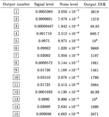
We assume the signal and noise levels at the inputs to be 1 and iOn, respectively (in arbitrary units). The correspond-ing signal and noise levels and SNRs at the outputs are given in Table 1.
The lowest output SNR occurred for path 12 and is equal to 40.99. Note that this is one of the longest paths and has the most number of bends. Remember that the noise level given in Table 1 does not include the thermal and shot noises associated with the detector and related circuitry. These can
Fig. 9 Example circuit with 15 paths and 320 segments.
Fig. 10 General step index channel waveguide.
Table 1 Output signal, noise, and SNR values of the example cir-cuit.
Output number Signal level Noise level Output SNR
Ij
0.0005369 2.050 x10⁷ 2619 II1 0.0009601 7.878 x10⁷ 12191
0.00009487 1.942 x10⁶ 48.85 0.001710 2.512 x10⁶ 680.7 EI1 0.9975 9.975 x10⁵i0
i1
0.09862 1.020 x10⁵ 9669 0.03092 5.950 x10⁶ 5197I1
0.0009572 5.144x10⁷ 1861 EI11 0.01736 1.188x10⁵ 1461 EI1 0.05510 3.078x10⁵ 1790 0.01735 3.413x10⁶ 5084E1
0.0001693 4.130x10⁶ 40.99I1
0.9990 9.990x10⁵ i04 EI1 0.03088 2.834x10⁵ 10901
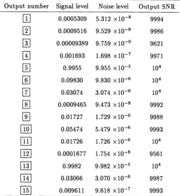
0.009696 4.682x10⁶ 2071 be easily accounted for, depending on the type of detector and circuitry used.The circuit design can be modified if some of the output SNRs are not large enough. A simple way of achieving this is to increase the separation between the waveguides. For instance, let us increase the minimum spacing between the nearest waveguides to five grid spacings (10 rim) in the pre-vious circuit. In this case, the coupling coefficient becomes
K 7.354
x
10_6m '.
The output signal and noise levels for this case are given in Table 2.Thepath with the minimum output SNR is again path 12, but the SNR is now 9561. This significant increase in the output SNR is a result of the ex-ponential dependence of coupling on the separation of the guides.A more intelligent (but much more involved) design pro-cedure would be to selectively increase the separation be-tween those guides that do not exhibit satisfactory SNR rather than increasing all separations uniformly as we have done earlier. Thus, it is possible to achieve a minimum circuit area for a specified SNR.
6
Conclusions, Discussion, and Future WorkWehave developed a method of analysis for integrated op-tical circuits of arbitrary topology. A system based on this method has been implemented. It calculates signal and noise
Table 2 Output signal, noise, and SNR values ofthe example circuit with increased grid spacing.
Output number Signal level Noise level Output SNR
0.0005309 5.312
x108
9994 0.0009516 9.529x10⁸
9986 0.00009389 9.759x10⁹
9621 0.001693 1.698x10⁷
9971 0.9955 9.955x10⁵
i04jJ
0.09830 9.830x1O6 i04 0.03074 3.074x10⁶
i0
0.0009465 9.473x10⁸
9992 0.01727 1.729x10⁶
9988 0.05474 5.479xlO6
9993 0.01726 1.726x10⁶
i04 0.0001677 1.754x10⁸
9561j1
0.9982 9.982x10⁵
i04 0.03066 3.070x10⁶
9987 0.009611 9.618x10⁷
9993levels at the output of each interconnect, given those at the input. Novel data structures and algorithms for storing and manipulating the circuit have been created in the process.
Because of its speed, our analysis system can be made the basis of a design system in a straightforward manner. One can start with a relatively densely packed circuit. After run-ning our analysis program, the spacing between interconnects that result in unsatisfactory SNRs and their neighbors can be increased. This process can be iterated until a satisfactory SNR is achieved for all interconnects. An alternative ap-proach would be to start from a well-spaced circuit, and then try to compact it using our analysis system.
Empirical studies of a large number of circuits can lead to several general design rules, as well as general guidelines, experience, and intuition as to how such circuits should be contemplated and laid out in the first place. This would be of great value, since design tools for systems of such com-plexity usually converge to local optima, and how close we are to the globally optimum circuit layout depends on the initial layout with which we start the optimization.
A useful measure of the packing density of any given
circuit is the ratio of the total area A to the total length of interconnections 1total' which can be interpreted as the effec-tive transverse width of interconnections, which also ac-counts for all inefficiencies in packing the lines. Normalizing by the wavelength of light used,
A
Weff 'total
The value of Weff for the circuit given in Fig. 9 is 3.86 for a minimum separation of 6 pm, and 6.44 for a minimum sep-aration of 10 m. (No effort has been made to compact this
circuit as much as possible.) Naturally, Weff cannot be made smaller than unity. In general, there will be a trade-off be-tween Weff and the SNR.
Apart from the developments suggested earlier, future work may include experimental verification of the results of the program for a trial circuit similar to that given in Fig. 9 and extension to circuits with fan-out and fan-in.
Acknowledgments
Weare gratefulto Ogan Ocali ofBilkent University for letting us benefit from his expertise in solving sparse matrix equa-tions and providing us with the necessary programs. We ex-tend our thanks to Tulay çora, Tuncer Demirel, and Baki Sahin, who did a major part of the programming. Their ef-ficient programming contributed to the speed of operation of our system. This research was sponsored by NATO's Sci-entific Affairs Division in the framework of the Science for Stability Programme.
References
1. J.W. Goodman, F. J. Leonberger, S. Y. Kung, and R. A. Athale, "Up-tical interconnections for VLSI systems,' ' Proc. IEEE 72, 850—866 (1984).
2. L. D. Hutcheson and P. Haugen, ''Opticalinterconnects replace hard-ware," IEEE Spectrum, pp. 30—35 (March 1987).
3. R.K. Kostuk, J. W. Goodman, and L. Hesselink, "Optical imaging applied to microelectronic chip-to-chip interconnections,' 'Appi.Opt. 24,2851—2858 (1985).
4.J. A. Neff, ''Majorinitiatives for optical computing," Opt. Eng. 26(10), 2—9(1987).
5.H. M. Ozaktas, ''Aphysical approach to communication limits in
com-putation," PhD Thesis, Stanford University (June 1991).
6. H. M Ozaktas and J. W. Goodman, ''Implicationsof interconnection theory foroptical digitalcomputing," Appi. Opt. 31, 5559—5567 (1992). 7. H. M. Ozaktas and J. W. Goodman, ''Thelimitations of interconnec-tions in providing communication between an array of pointers,' 'in
Frontiers of Computing Systems Research, pp. 61—1 30, Plenum Press, NewYork (1991).
8. M. R. Feldman, S. C. Esener, C. C. Guest, and S. H. Lee, ''Comparison
between optical and electrical interconnects based on power and speed considerations," Appi. Opt. 27, 1742—1751 (1988).
9. F. E. Kiamilev, P. Marchand, A. V. Krishnamoorthy, S. C. Esener, and S. H. Lee, ''Performancecomparison between optoelectronic and VLSI multistage interconnection networks,' ' J. Lightwave Technol. 9,
1674—1692(1991).
10.H. B. Bakoglu, Circuits, Interconnections and Packaging for VLSI,
Addison-Wesley, Reading, MA (1990).
11. P. R. Haugen, S. Rychnovsky, A. Husain, and L. D. Hutcheson,
"Up-tical interconnects for high speed computing," Opt. Eng. 25(10),
1076—1085(1986).
12.K. C. Saraswat and F. Mohammadi, ' 'Effect of scaling of
interconnec-tions on the time delay ofVLSI circuits,' ' IEEE Trans. Electron Devices 29,645—650(1982).
13. J. W. Parker, ''Opticalinterconnection for advanced processor systems:
a review of the ESPRIT 2 OLIVES program,' 'J.Lightwave Technol. 9, 1764—1773 (1991).
14.H. Kogelnik, "Theory of optical waveguides," in Guided-Wave
Opto-electronics, Chap. 2, T. Tamir, Ed., Springer-Verlag, Berlin (1988). 15. W. Stutius and W. Streifer, ''Siliconnitride films on silicon for optical
waveguides," Appl. Opt. 6, 3218—3222 (1977).
16. J. M. Trewhella et. al, ''Polymericoptical waveguides,' 'Proc.SPIE 1177,379—386 (1989).
17.B. L. Booth, ''Lowloss channel waveguides in polymers,' 'J.Lightwave
Technol. 7, 1445—1453(1989).
18.C. S. Li, C. M. Olsen, and D. G. Messerschmitt, "Analysis of crosstalk
penalty in dense optical chip interconnects using single-mode wave-guides,' 'J.Lightwave Technol. 9,1693—1701(1991).
19. Y. Chung and N. Dagli, ''An assessment of finite difference beam
propagation method,' ' IEEEJ. Quantum Electron. 26, 1335—1339 (1990).
(11) 20. R. Boult, ''Simulationsoftware aids optoelectronic research,' ' Light-wave, PennWell Books, p. 14 (Mar. 1993).
21. C. Mead and L. Conway, Introduction to VLSI Systems, Addison-Wesley, Reading, MA (1980).
22. H. M. Ozaktas, ''Researchdirections in integrated guided wave optical
interconnects,' 'InternalReport, Information Systems Laboratory,
Stan-ford University, Palo Alto, CA (May 1989).
1 602 IOPTICAL ENGINEERING I May 1 994 I Vol. 33 No. 5
Downloaded from SPIE Digital Library on 20 Oct 2010 to 66.165.46.178. Terms of Use: http://spiedl.org/terms
Downloaded From: https://www.spiedigitallibrary.org/journals/Optical-Engineering on 1/28/2019 Terms of Use: https://www.spiedigitallibrary.org/terms-of-use
23. R. Sims and J. Cozens, Optical Guided Waves and Devices, McGraw-Hill, Shoppenhangers Road, Maidenhead, Bershire, England (1992). 24. A Yariv, Quantum Electronics, John Wiley & Sons, New York (1989). 25. W. K. Burns and A. F. Milton, ''Waveguidetransitions and junctions," in Guided-Wave Optoelectronics, Chap. 3, 1. Tamir, Ed., Springer-Verlag, Berlin (1988).
26. K. Kishioka, ''Improvementof the power spectral response in the three-guided coupler demultiplexer," AppI. Opt. 29, 360—366 (1990). 27. Gurkan Onal, ''Computeraided analysis and simulation of complex
passive integrated optical circuits,' ' Master'sThesis, Bilkent Univer-sity, Ankara, Turkey (1993).
28. A. W. Snyder and J. D. Love, Optical Waveguide Theory, Chapman and Hall, New York (1983).
29. G. Onal, A. Altintas, and H. Ozaktas, ''Astudy of development of design rules for photonic chips,' 'inLightwave Technology and Com-munications, A. Altintas and G. Saplakoglu, Eds., pp. 235—241, Bilkent University, Ankara, Turkey (July 1992).
30. R. J. Black and C. Pask, "Equivalent optical waveguides," J. Lightwave Technol. 2, 268-276 (1984).
31. T. K. Findakly, "Optical channel waveguides and waveguide cou-plers," in Handbook of Microwave and Optical Components, Chap. 2, K. Chang, Ed., John Wiley & Sons, New York (1989).
GUrkanOnal received his BS and MS
de-grees from the Department of Electrical and Electronics Engineering, Bilkent Uni-versity, Ankara, in 1991 and 1993, respec-tively. He is currently studying for his PhD degree and is working as a research as-sistant in the same university. His interests include optical systems and integrated optics.
Ayhan AItinta received his BS and MS
degrees from the Middle East Technical
University (METU), Ankara, Turkey, in 1 979 and 1 981 , respectively, and the PhD degree from Ohio State University, Colum-bus, in 1986, all in electrical engineering.
From 1981 to 1987, he was with the ElectroScience Laboratory, Ohio State
University. He then spent one year at the Optical Sciences Center of The Australian National University, Canberra. Currently, he is an associate professor at the Department of Electrical and Electronics Engineering, Bilkent University, Ankara, Turkey. His re-search interests are in electromagnetic radiation and scattering, mi-crowaves, fiber optics, and integrated optics. Dr. Altinta is a senior member of IEEE and a member of Sigma Xi and Phi Kappa Phi. He is the recipient of the ElectroScience Laboratory Outstanding Dis-sertation Award of 1986, the IEEE 1991 Outstanding Student Branch Counselor Award, and the 1991 Research Award of the Professor Mustafa N. Parlar Foundation of METU.
Haldun M. Ozaktas received a BS degree from the Middle East Technical University, Ankara, Turkey, in 1987 and MS and PhD degrees from Stanford University, Califor-nia, in 1988 and 1991, respectively, all in electrical engineering. His academic inter-ests include optical information process-ing, optical interconnections, and signal processing. He is currently an assistant professor of electrical engineering at Bilk-ent University, Ankara, Turkey.