INSTITUTE OF NATURAL AND APPLIED SCIENCE
THE INFLUENCE OF SUBSTRATE TEMPERATURE ON
ELECTRICAL PARAMETERS OF REACTIVE
SPUTTERED Cr
2O
3/n-Si HETEROJUNCTIONS
ALI A. ISSA
MASTER THESIS DEPARTMENT OF PHYSICS
DİYARBAKIR June 2015
T.R.
DICLE UNIVERSITY
INSTITUTE OF NATURAL AND APPLIED SCIENCE
THE INFLUENCE OF SUBSTRATE TEMPERATURE ON
ELECTRICAL PARAMETERS OF REACTIVE
SPUTTERED Cr
2O
3/n-Si HETEROJUNCTIONS
ALI A. ISSA
SUPERVISED BY
ASSOC. PROF. DR. YUSUF SELIM OCAK
MASTER THESIS DEPARTMENT OF PHYSICS
DİYARBAKIR June 2015
i
Acknowledgment
I introduce this work as a graduated thesis in Institude of Science and Technology in Dicle university under the supervision Assoc. Prof Dr.Yusuf Selim Ocak . I want to thank him because of his supervision on my master study.
My sincere thanks to my lecturar who taught me Assoc. Prof. Dr. Omer Celik and also the Research Assistant Dr.Ahmet Tombak of his supporting me during experimental procedures. I am also grateful to the Director of the labratory prof. Dr. Hamdi Temel.
And also I want to thank all those who participated to facilitate our study in Turkey and especialy Dicle University in Diyarbakir.
I am greateful to my family for their moral support and their encouragement me during my study.
ALI AHMED ISSA May 2015
ii CONTEXT ACKNOWLEDGEMENT... i CONTEXT... ii ÖZET...iv ABSTRACT...v LIST OF TABLES...vi LIST OF FIGURES...vii
ANNOTATION AND SYMBOLS...viii
1. INTRODUCTION...1
2. LITERATURE SUMMARY...5
3. MATERIAL AND METHOD...11
3.1 Metal-Semiconductor Contacts...11
3.1.1 Rectifying Contacts...12
3.1.2 Ohmic Contacts...13
3.2 Physical Vapor deposition Methods...14
3.3 Optical Properties of Materials...16
3.3.1 Absorbance...16
3.3.1.1 Direct band transition...17
3.3.1.2 Indirect band transition...18
3.3.2 Transmittance...19
3.4 Experimental procedures...21
3.4.1 Formation of ohmic contact...21
3.4.2 Deposition of Cr2O3 thin film...22
3.4.3 Formation of front contact and measurements...23
4. FINDING AND DISCUSSION...27
4.1 Introduction...27
4.2 Optical properties of Cr2O3 Thin Film on a glass...27
4.3 current-voltage properties of Cr2O3/n-Si heterojunction...28
iii
5. RESULTS AND SUGGESTION...37 6. REFERENCE...39
iv ÖZET
REAKTİF SAÇTIRMA YÖNTEMİ İLE OLUŞTURULAN Cr2O3/n-Si HETEROEKLEMLERİN ELEKTRİKSEL ÖZELLİKLERİNE ALTTAŞ
SICAKLIĞININ ETKİSİ
YÜKSEK LİSANS TEZİ
Ali Ahmed ISSA
DİCLE ÜNİVERSİTESİ FEN BİLİMLERİ ENSTİTÜSÜ
FİZİK ANABİLİM DALI
2015
Bu çalışmada, alttaş sıcaklığının Cr2O3/n-Si heteroeklemler üzerine etkisini incelemek amaçlanmıştır. Bu amaçla, Cr2O3 ince filmleri 40, 150 and 250 °C alttaş
sıcaklıklarında radio frekansı (RF) reaktif saçtırma yöntemi ile n-Si ve cam alttaşlar üzerine büyütülmüştür. Yüksek saflıktaki Cr metali hedef ve oksijen ise reaktif gaz olarak kullanılmıştır. Cr2O3 ince filmlerin optic özellikleri uv-vis verileri ile incelenmiştir. Cr2O3/n-Si heteroeklemlerin elektriksel özellikleri karanlıkta akım-gerilim (I-V) ölçümleri ile incelenmiştir. 250 °C alttaş sıcaklığında büyütülen Cr2O3 ince filmleri ile oluşturulan Cr2O3/n-Si heteroeklemin mükemmel doğrultmaya sahip olduğu görülmüştür. Bu yapının idealite faktörü, engel yüksekliği ve seri direnç gibi elektriksel özellikleri I-V verileri ile hesaplanmıştır. Işık şiddetinin bu yapının fotovoltaik parametreleri üzerin etkiside incelenmiştir. Son olarak, kapasite gerilim ölçümleri ile elde edilen engel yüksekliği değeri I-V ile elde edilen değer ile karşılaştırıldı.
v ABSTRACT
THE INFLUENCE OF SUBSTRATE TEMPERATURE ON ELECTRICAL PARAMETERS OF REACTIVE SPUTTERED Cr2O3/n-Si HETEROJUNCTION
MSc THESIS
Ali Ahmed ISSA
DEPARTMENT OF PHYSICS
INSTITUTE OF NATURAL AND APPLIED SCIENCES UNIVERSITY OF DICLE
2015
The purpose of this study was to see the effects of substrate temperature on Cr2O3/n-Si heterojunctions. For this purpose Cr2O3/n-Si thin films were formed on n.Si and glass substrates at 40,150 and 250 C° by radio frequency (RF) reactive technique. High purity Cr was used as target and oxygen was used as reactive gas.
Optical properties of Cr2O3/n-Si thin films were analyzed using Uv-vis data . The band gaps of the films were compared.
The electrical properties of Cr2O3/n-Si heterojunction were tested by their current voltage (I-V) measurements in dark. It was observed that the heterojunction which was fabricated by forming Cr2O3 thin film at 250 °C gave better rectification.
The characteristics electrical parameters such as barrier height, ideality factor and series resistance were calculated by using its I-V data. The influence of light intensity on photovoltaic effect behavior of the device was also calculated, finally the barrier height value of the structure obtained from capacitance-voltage (C-V) data were compared with the one calculated from I-V measurements.
vi
LIST OF TABLES
Table 1. Some electrical parameters of Cr2O3/n-Si heterojunction at room
temperature...30 Table 2. Photoelectrical parameters of Cr2O3/n-Si heterojunction...33
vii
LIST OF FIGURES
Figure. 1.1 Crystal structure of Cr2O3...2
Figure 2.1 A SEM image of a perovskite based heterojunction solar cell...7
Figure 2.2 The cross section image of ZnO/p-InP heterojunction heterojunction...8
Figure 3.1 Energy band diagram of metal-n-type semiconductor a) before the formation of a contact b) after formation of a contact...13
Figure 3.2. Ohmic and Schottky contact plots...14
Figure 3.3. Diagrams of sputtering and thermal evaporation processes...15
Figure 3.4 Absorption in a thin film...16
Figure 3.5 Representation of the direct and indirect transition through band gap...17
Figure 3.6 The annealing furnace used in the study...22
Figure 3.7. Nanovak NVTS 400 vaccum system...23
Figure 3.8. The cross section illustratioon of Au/ Cr2O3/n-Si diode...24
Figure 3.9a. Current-voltage measurement system with Keithley 2400 sourcemeter and Oriel solar simulator...24
Figure 3.9b. Capacitance-voltage measurement system with Agilent 4294 A Impedance analyzer...25
Figure 3.10. Shimadzu 3600 Uv-vis-nir spectrophometer...25
Figure 4.1. Absorbance vs. wavelength plot of Cr2O3 thin films on glasses...27
Figure 4.2. (Ahʋ)2-hʋ plots of Cr2O3 thin film on aglass...28
Figure 4.3. lnI-V plots of Cr2O3/n-Si heterojunctions obtained various substrate temperature...29
Figure 4.4. F(V)–V curve of Au/Cr2O3/n-Si heterojunction...31
Figure 4.5. lnI-V plots of Cr2O3/n-Si heterojunction in dark and various illumination conditions...32
Figure 4.6. C-V plots of Au/Cr2O3/n-Si heterojunction for various frequencies...34
viii ANNOTATION AND SYMBOLS
MS Metal-Semiconductor contacts
MIS Metal-Insulator-Semiconductor contacts V Voltag
I Current
I-V Current-voltage characteristic q Electron charge
qx Electron affinity T Absolute Temperature K Kelvin
RF Radio Frequency LEDs Light emitting diodes P-Si p-type of Silicon N-Si n-type of silicon UV Ultra violet
PVD Physical vapor deposition CVD Chemical vapor deposition Φs Work function of semiconductor Φm Work function of metal
Φb Barrier high
Φbe Barrier high of p-type Φbn Barrier high of n-type Eg Band gap x Distance Rs Series resistance Ω Ohm k Boltzman constant αs Absorption coefficient
ix αe Emissions coefficient
Ei Initial state of energy Es Final state of energy EPH Phonon energy h Plank's constant ʋ Frequency
me* Effective mass of electron mh
*
Effective mass of hole T Transmittance A Absorption R Reflection A Diode Area A* Richardson constant F(V) Norde function
εs Dielectric constant of semiconductors εs The dielectric constant of the cavity
E Intensity of light passing through the thin film Eo Intensity of incident light
PL Photoluminescence AM Air mass
AFM Atomic force microscopy XRD X-ray diffraction
1 1. Introduction
In general materials can be divided into three parts according to their electrical properties. These are conductors, semiconductors and insulators. Electrical conductivity of semiconductors decreases with decreasing temperature. This property is opposite of the conductors. The modern technology directly built on semiconductors because of the possibility to modify their electrical and optical properties by adding impurities and oxidation. There are many kinds of electrical and optical devices built in using semiconductor technology including solar cells, light emitting diodes, transistors, physical and chemical sensors. There are several types of junctions such as metal-semiconductor (MS) contacts, metal-insulator-metal-semiconductor (MIS) contacts, p-n junctions and heterojunctions used in modern semiconductor technology.
Although the MS contact is the first discovered device, p-n junctions and heterojunctions started to play an important role in semiconductor industry. Most of the optoelectronic devices such as solar cells, light emitting diodes and sensors are fabricated using p-n junctions.
The p-n junctions can be divided in two parts; homojunctions and heterojunctions. Homojunction is a contact fabricated different conductivity types of same semiconductor such as n-Si/p-Si and n-InP/p-InP. Heterojunction is formed by joining two different semiconductors such as n-Si/p-GaAs and n-Si/n-GaAs. When the types of the conductivity are same, the contact is called isotype heterojunction and when the types of the conductivity are different, the contact is called anisotype heterojunction. In general different semiconductors have different band gaps. Therefore, there is a discontinuity of energy bands at the interface. Because of this discontinuity the current-voltage (I-V) characteristics of heterojunctions are different from conventional p-n junctions (Neamen and Pevzner 2003).
In the fabrication of semiconductor devices, there are many conditions which affect the physical, structural, morphological, optical and electrical properties. Substrate temperature, power applied to target, base pressure, ratio of the gasses in the chamber, working pressure, deposition rate and duration of the process can be accepted as examples.
1.INTRODUCTION
2
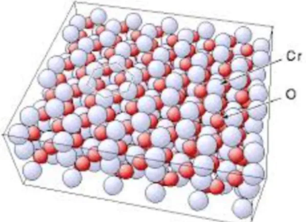
There are many studies to understand current-transport mechanisms of heterojunctions formed using different semiconductors. Chromium(III) oxide (Cr2O3) is one of the wide band gap inorganic semiconductor. It is a hard material and antiferromagnetic up to 307 K (Brockhouse 1953). It is also nearly unreactive to acids and bases.
Fig. 1.1 Crystal structure of Cr2O3
Up to now, Cr2O3 has been used in the fabrication of gas sensor to detect hydrogen, oxygen and nitrogen oxide (Lin, Takao et al. 1995; Hao, Yuan et al. 2006; Yoo and Wachsman 2006). The usage of the Cr2O3 in the fabrication of heterojunction has been also reported (Mostovoi, Brus et al. 2014). Cr2O3 thin films also shows high hardness and low friction coefficient. Therefore, it has been used instead of metal nitrides as hard material.
There are many ways to obtain a thin film of materials including spin coating, ultrasonic spray, thermal evaporation, pulsed laser deposition, electron beam, cathodic arc deposition and molecular beam epitaxial. It is very difficult to form thin films of refractory metals or ceramics. Magnetron sputtering technique is a unique method to obtain uniform thin films of ceramics refractory metals or ceramics.
In this study, it was aimed to see effects of substrate temperature on Cr2O3/n-Si heterojunctions. For this aim, Cr2O3 thin films were grown on n-Si and glass substrates at 40, 150 and 250 °C by radio frequency (RF) sputtering technique. High purity Crwas used as target and oxygen was used as reactive gas. Optical properties of properties of Cr2O3 thin films were analyzed using uv-vis data. The band gaps of the films were
3
compared. The electrical properties of Cr2O3/n-Si heterojunctions were examined by their current-voltage (I-V) measurements in dark. It was seen that the heterojunction fabricated by forming Cr2O3 thin film at 250 °C gave excellent rectification. The characteristics electrical parameters such as ideality factor, barrier height and series resistance were calculated using its I-V data. The effect of light intensity on photovoltaic behavior of the device was also examined. Finally, the barrier height value of the structure obtained from capacitance-voltage (C-V) data were compared with the one calculated from I-V measurements.
1.INTRODUCTION
4
5 2. LITERATURE SUMMARY
Nowadays, most of the main personel requirements are provided by modern technology. Revelotionary changes occur in our daily lives by the usage of new technological equipments. The main technological tools are based on electrical and optical devices. All electrical and optical devices are fabricated using various combinations of materials.
The first electronic device discovered over than 100 years by Braun . He found the asymetry in electrical conductivity of metal/semiconductor (MS) contacts formed using metal sulfate crystals. Jagadis Chandra Bose presented the usage of lead sulfide/metal rectifier to detect radio signals.
The first principal study on rectifying properties of MS contact was performed by Schottky, Sörmer and Waibel in 1931. They said that the rectification property of can occur owing to the potential drop across all contacts when current flows in the contact. After this study, Wilson developed the theory of quantum mechanical tunneling and explained the rectification using reverse polarity.
1938, Schottky and Mott indipendently suggested that rectification mechanism can be explained electron flows and diffusion over potential barrier. According to Schottky-Mott theory, existence of potential barrier is result in differences between metal and semiconductor work functions. Thus, greatness of potential barrier can be calculated using the differences between metal work function and semiconductor electron affinity. But, the experiments showed that barrier height is approximetly independent from metal work functions and its related to preperation methods. It was conculated from experimental results that theory was insufficient because it didn’t take the existance of a layer at MS interface into account. The fact that this layer is always possible in practice and prepration conditon can manipulate its thickness and chemical structure.
Main electrical properties of including barrier height and ideality factor values can be calculated using current-voltage (I-V) plot a structure. According to Mönch ideality factor of a MS contact should be 1.01 when image force lowring of Schottky potential taking into acoount (Mönch 2014). One of the esential parameters of rectifying diodes are series resistance, Norde proposed a method to calculate both barrier height
2. LITERATURE SUMMARY
6
and series resistance of non-ideal diode using its forward bias I-V characteristics (Norde 1979). Then, Cheung and Cheung reported another way to calculate barrier height, ideality factor and series resistance of both ideal and non-ideal diodes using its forward bias I-V data(Cheung and Cheung 1986).
The first p-n junction fabricated forming intimate contacts of n-Si and p-Si by Ohl and Jack Scaff in 1940s. In 1948, William Shockley's fabricated the first transistor using Ohl's serendipitous. These studies became the milestones for semiconductor industry.
In general, heterojunctions fabricated using two semiconductors with different band gaps are one of the most desired semiconductor based devices to benefit from both electrical and optical properties of semiconductors. Heterojunctions are the basis of many electrical or optical devices including room temperature injection laser, light emitting diodes (LEDs), photodiodes and solar cells.
Thin film heterojunction diodes using materials CdTe, Al2O3, and SiOx as insulating materials between CdS and metallic electrode was reported (Muller and Zuleeg 1964). They presented an excellent rectification of CdTe, Al2O3, and SiOx based heterojunctions.
Up to know many kinds of materials including organic and inorganic semiconductors have been used to control electrical and photoelectrical properties of heterojunction devices.
Si has indirect band gap. Therefore the thickness of Si based solar cells are about 200 µm. B O'regan and M Grätzel (1991) presented the large-scale use of photovoltaic devices for electricity generation using a low cost and easy method. They formed organic-inorganic heterojunction device using TiO2 colloidal TiO2 films and a Ru(II) complex. They developed the first dye sensitized solar cell (DSSC) structure about 10-µm-thick with 12% power conversion efficiency (O'regan and Grätzel 1991).
After Gratzel many studies have been performed on organic-inorganic heterojunction solar cells. In 2009, first study published on perovskite structured compounds in the fabrication of heterojunction solar cells with 3.8 % efficiency (Kojima, Teshima et al. 2009). Organic-inorganic Perovskite materilas such as methylammonium or formamidinium lead halides based solar cells are cheap to produce
7
Fig 2.1 A SEM image of a perovskite based heterojunction solar cell.
and simple to manufacture. Therefore, many studies have been performed to improve the efficiency of perevskite based solar cells. In 2014, a prevskite solar cell with 20.1 % efficiency was certified. This is the fastest-advancing solar technology up to date (Green, Emery et al. 2015).
p-ZnGa2Se4 thin film was deposited onto n-Si substrate by means of thermal evaporation technique using high purity Zn, Ga and Se metals and annealed at 700 K (Yahia, Fadel et al. 2011). They fabricated Al/p-ZnGa2Se4/n-Si/Al heterojunction by forming Al contact to p-ZnGa2Se4 thin films. They analyzed the electrical properties of the heterojunction using current-voltage measurements of the device between 303 and 423 K. They calculated main electrical properties using lnI-V and Norde plots. They reported that the reverse bias current properties of the structure were controlled by the carrier generation–recombination process in the depletion region. They supposed that the Al/p-ZnGa2Se4/n-Si/Al diode was a good candidate for electrical applications.
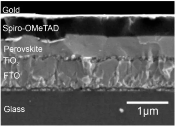
Ocak et al (2011) fabricated a ZnO/p-InP heterojunction structure by sputtering of 50 nm ZnO compound on p-InP substrate. They used Au–Zn (90–10%) alloy as back contact and Al metal as front contact. They determined the electrical parameters of the device in dark in the range of 300–380 K using its current-voltage measurments. They also reported the photovoltaic properties of ZnO/p-InP heterojunction between 40 and 100 mW/cm2 with 20 mW/cm2 intervals using a solar Simulator with AM.1.5 global filter (Ocak, Kulakci et al. 2011).
Chromium oxide with Cr2O3 formula is a wide band p-type semiconductor. It has been used as protective coating because of its outstanding wear resistance. Kao et al
2. LITERATURE SUMMARY
8
Fig 2.2 The cross section image of ZnO/p-InP heterojunction heterojunction
(1989) formed Cr2O3 thin films by sputtering of Cr2O3 thin films for various substrate temperatures. It was showed that the Cr2O3 thin films formed at 150 ⁰C in pure argon annelaed at 300 ⁰C had thee hardness about 25 GPa (Kao, Doerner et al. 1989).
Gas sensing properties of Cr2O3 has been studied for different gases. For instance, Stanoiu et al (2012) obtained Cr2O3 nanoparticles by the help of the hydrothermal reaction and heating 500-700 ⁰C. They characterize the nanoparticles using XRD and TEM techniques. They reported the usage of Cr2O3 to sense NO2 and CO in dry and humid air (Stănoiu, Simion et al. 2012).
Erdogan and Gullu (2011) obtained Cr2O3 nanoparticles by hydrothermal technique. They formed Cr2O3 thin film on p-Si substrate by spinning using nanoparticle solution and annealed at 500 °C for 1 h. They studied optical, morphological and structural properties thin film. They used x-ray diffraction (XRD), non-contact atomic force microscopy (AFM), ultravioltet-visible spectroscopy (uv-vis) and photoluminescence (PL) spectroscopy. They reported that the thickness of the film is about 70 nm and the band gap of the film is 3.08 eV. They also formed Au/Cr2O3/p-Si metal-insulator-semiconductor (MIS) diodes to determined electronic parameters by means of I-V nad C-V data. They calculated ideality factor and barrier height of the device as 2.14 and 0.74 eV, respectively. They also calculated interface state density distribution of the diode (Erdoğan and Güllü 2010).
Formation of thin films to fabricate heterojunctions can be performed using many kinds of techniques such as spin coating, ultrasonic spray, thermal evaporation, pulsed laser deposition, electron beam and magnetron sputtering. It is very difficult to form thin films of refractory metals or ceramics. Magnetron sputtering technique is a unique method to obtain uniform thin films of ceramics refractory metals or ceramics.
9
In this study, Cr2O3 thin films were formed on n-Si semiconductor and substrate by means of reactive sputtering technique at 40, 150 and 250 °C. A cromium metal target used as source and O2 used as reactive gas. Optical properties of the thin films were determined using UV-vis data. Au metal was evaporated on Cr2O3/n-Si structures. Electrical properties of the Cr2O3/n-Si heterojunctions were examined using their I-V measurements in dark at room temperature. It was seen that the device obtained using the Cr2O3 formed at 250 °C gave an excellent rectification property. The characteristic electrical paramaters including barrier height, ideality factor and series resistance of the rectifying diode were determined. The effect of the light on photoelectrical parameters such as sensitivity to light, open circuit voltage and short circuit current were determined for various illumination intensities. Furthermore, capacitance-voltage properties of the structure were also analyzed.
2. LITERATURE SUMMARY
10
11 3. MATERIALS AND METHODS
In this study, it was aimed to see effects of substrate temperature on Cr2O3/n-Si heterojunctions. For this aim, Cr2O3 thin films were grown on n-Si and glass substrates at 40, 150 and 250 °C by radio frequency (RF) sputtering technique. High purity Crwas used as target and oxygen was used as reactive gas. Optical properties of properties of Cr2O3 thin films were analyzed using uv-vis data. The band gaps of the films were compared. The electrical properties of Cr2O3/n-Si heterojunctions were examined by their current-voltage (I-V) measurements in dark. It was seen that the heterojunction fabricated by forming Cr2O3 thin film at 250 °C gave excellent rectification. The characteristics electrical parameters such as ideality factor, barrier height and series resistance were calculated using its I-V data. The effect of light intensity on photovoltaic behavior of the device was also examined. Finally, the barrier height value of the structure obtained from capacitance-voltage (C-V) data were compared with the one calculated from I-V measurements.
In this chapter, firstly the physics of MS structures, the conduction mechanisms in these contacts and the factors which affect physical parameters of devices will be given. Then, physical vapor deposition (PVD) systems which were used in this study will be discussed. Optical properties of materials will be also discussed in this chapter.
Finally, at the end of the chapter, all experimental parts of this study will be explained in detail.
3.1. Metal-Semiconductor Contacts
Metal semiconductor (MS) contacts have great importance because they are used in the fabrication of all kinds semiconductor based electronic devices. MS contacts can be examined in two different parts as ohmic contacts and rectifying Schottky contacts. In this part, formation of MS structures, conduction mechanisms of these structures and determination of electrical properties will be discussed.
When a metal and semiconductor make a contact without any material between them it is called as MS contact. Theoretically, if the work function of semiconductor is larger than the work function of metal (m<s), it forms rectifying contact and if the work function of metal is larger than the work function of semiconductor (s<m), it forms ohmic contact for p-type semiconductors. For the n-type semiconductor it is just the opposite.
3.MATERIALS AND METHODS
12 3.1.1. Rectifying Contacts
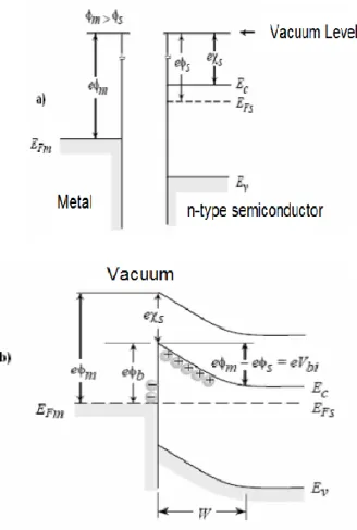
Work function of metal is expressed as qm and it is equal to q(χ+n) where qχ is electron affinity which defined as the difference between the bottom of the conduction band the vacuum level. The contact potential is defined as the difference between two work functions (m-(χ+n)). When the distance between metal and semiconductor is decreased, electric field in this region increases and decreasing negative carrier occurs. A positive carrier should be created at depletion region. The potential difference is very similar to one side of p-n junction. If the distance is very small, this region becomes transparent for electrons and the situation shown in Fig. 3.1 occurs. For an ideal contact between a metal and a p-type semiconductor, barrier height is written as (Rhoderick and Williams 1988)
bnq m q 3.1
bpEg q m q 3.2Therefore, sum of the barrier heights of a MS contact formed using a metal and p-type and n-type semiconductor is equal to band gap of the semiconductors.
bp bn
g q
E 3.3
For a MS contact formed using an n-type semiconductor, ionized donors (positive carriers) in semiconductor side of contact are space charges because they are motionless. When a reverse potential applied to contact, barrier height doesn’t change for electrons which wants to pass to barrier. For this reason, current flow from semiconductor to metal becomes constant. On the other hand, for electrons pass from metal to semiconductor barrier height decreases about eV value and current flow from metal to semiconductor decreases as exp(eV/kT) factor. Therefore, the net current can be expressed as (Rhoderick and Williams 1988)
nkT IR V q I I ( s) exp 0 3.4
Where I is the current, I0 is the current q is the electron charge, V is the applied voltage, n is the
ideality factor, k is the Boltzmann constant T is the absolute temperature. For this equation, net current is positive and this situation is called as forward bias. When a positive voltage applied to semiconductor, conduction band decreases about eV and barrier height in the semiconductor side increases about eV. This situation is called as reverse bias.
13
Fig 3.1 Energy band diagram of metal-n-type semiconductor a) before the formation of a contact b) after formation of a contact
3.1.2 Ohmic contacts
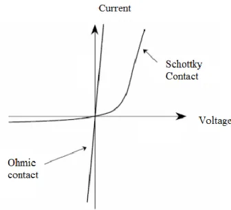
The main aim to use ohmic contacts is to get or give current to semiconductor with minimum resistance. Ohmic contact obeys the ohm law. The quality of the ohmic contact is related to contact resistance. This resistance is written as
1 0 V C V I R 3.5
3.MATERIALS AND METHODS
14
Fig 3.2. Ohmic and Schottky contact plots
3.2. Physical Vapor Deposition Methods
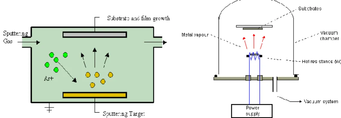
The main methods for depositing thin films are evaporations and sputtering, so the concentration will be on the explanation of these methods in this chapter. The aim which stands behind the process of deposition is to make a control on the transfer of atoms from the source to subtract where film consistence and outgrowth progress atomistically. During the process of evaporation, atoms are separated from the source due to thermal means but in the process of sputtering, they are expelled from solid target surface due to the effect of gaseous ions. The beginning experimentation of these kinks of deposition techniques can be obviously influence to same period of the nineteenth century. Grove (Grove 1852) AC realize sputtering of metal deposits from cathode of an illumination discharge. Faraday, after five years, testing with exploding fuse like metal in a static atmosphere, fabricated evaporated thin films. With the progress and evolution of vacuum pumping instrument and manufacturing of suitable Joule heating sources such as which made from platinum and tungsten wire, supported the progress of evaporation technology. The scientific advantage in the phenomenon of evaporation and the characteristics of thin films of metal was followed up by industrial output of optical components like beam splitters, mirrors, and antireflection coatings. Sputtering was utilized in 1877 to coat mirrors, and its usages included coating of flimsy construction with Au and deposition of metal films on record rules of
15
phonograph records before to thickening Up to the late of 1960s, evaporation obviously exceeded sputtering as the favorite film deposition technique. Higher deposition average, superior vacuum, and cleaner environments for film consistence and outgrowth, and general usable to all categories of materials were some of the reasons for dominance of evaporation methods. Films are used for magnetic and microelectronic applications required the usage of alloys, with severe stoichiometry limits, which ought to adapt cover and abide well to substrate surfaces. These requests plus the introduction of radio frequency (RF), bias and magnetron varians that spread the power of sputtering and availability of high purity targets and working gases, assisted prefer the popularity of sputter deposition.
According to special implementations to evaporate or sputter thin films is not always clear and has encouraged a lively competition among these methods. On the other hand, characteristics of evaporate and sputter have been fabricated into mongrel operation. The basic film deposition methods treated in this thesis are physical vapor deposition(PVD), the expression that includes evaporation and sputtering, and chemical vapor deposition (CVD) will all of variant and mongrel operations.
The following are some factors which differentiate PVD from CVD 1. Dependence on solid or molten sources.
2. Physical techniques (evaporation or collisional affect) by which source atoms get in the gas phase.
3. Reducing pressure environment through which the gaseous sort are transported. 4. Overall nonattendance of chemical reactions in the gas phase and at the substrate
surface (PVD reactive processes are exclusion).
3.MATERIALS AND METHODS
16 3.3. Optical Properties of Materials 3.3.1. Absorbance
Absorption is called energy loss of an incident electromagnetic wave to a crystal plane by interacting with the electrically charged particles. The most commonly used method for determining forbidden energy band gap of semiconductors is optical absorption method. A photon coming to a semiconductor excites an electron from low energy level to a high energy level in absorption process. The correlation between incident and transmitting of beam light coming through the thin film with a thickness x is as follows
x e E
E 0 3.6
where E0 the intensity of the incident light, E intensity of light passing through the thin film, x is thin film thickness and α is absorption coefficient of the material used (semiconductor).
Fig 3.4 Absorption in a thin film
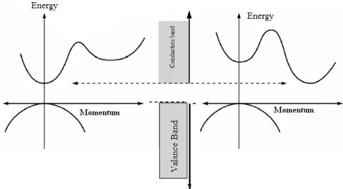
There are two types of band transition in crystalline and amorphous semiconductors. These are direct and indirect band transition and shown in the figure3.5. Direct transition state occurs when the momentum of minimum valance band is the same as conduction band momentum. In Figure 3.5, the electron absorbs a photon without a change in its momentum value and transmits from valence band to the conduction band with energy received from the photon. The minimum valance band energy is different from that of the conduction band maximum energy for the material having an indirect band gap. Electrons in the conduction band go down to the minimum band energy quickly. In the same way, holes reach the maximum of valance band. Therefore, momentum of electrons and holes is the same for a direct transition semiconductor while is not the same for indirect transition
17
Fig 3.5 Representation of the direct and indirect transition through band gap
semiconductor. This result is because of the lifetime of minority charge carriers and optical properties.
3.3.1.1. Direct band transition
When a photon with energy hν comes to a direct band gap semiconductor, an electron jumps from the valence band to the conduction band. Ei is initial state in semiconductor, Es is the final energy state. Therefore, the energy difference,
i s E
E
h
3.7
is given by the equation. In the parabolic band,
* 2 2 e g s m p E E 3.8 and * 2 2 h i m p E 3.9
is determined by the expressions. Where me* the effective mass of the electron and mh* is effective mass of hole. If equations 3.32, 3.33 and 3.34 are arranged
3.MATERIALS AND METHODS 18 2 1* 1* 2 e h g m m p E h 3.10
is obtained by correlation. In direct band transition relation between α and hν is;
m g E h h ( ) 3.11 is given by the equation. Κ is constant, m is a constant, which can take 1/2 for, allowed transition or 3/2 forbidden transition values. In addition, in equation 3.8 the value making zero of the parenthesis gives the forbidden energy gap value of the semiconductor which is equal to αhν.
3.3.1.2 Indirect band transition
Because the momentum of the electrons of valance band maximum and conduction band minimum, in order to conserve momentum of the electrons, photon absorption event should contain additional particles. In this case, either emission or absorption of a photon for momentum conservation is required. The phonon
absorption coefficient
1 ) / exp( ) ( kT E E E h h ph m ph g s 3.12 and
) / exp( 1 ) ( kT E E E h h ph m ph g e 3.13can be written. Here
sis absorption coefficient and
eis emission coefficient, Eph is the phonon energy. It is also possible for both possibilities) ( ) ( ) (
h s h e h 3.14can be written. When it is clearly written
) / exp( 1 1 ) / exp( ) ( kT E E E h kT E E E h h ph m ph g ph m ph g 3.1519
Where m is a constant, which can take 2 allowed or 3 forbidden transition values for an indirect band gap semiconductor.
3.3.2. Transmittance
Transmittance is defined as the ratio of the intensity of light incident on the sample to the intensity of light passing through a sample and expressed by the equation
E T
Eo
3.16 Both transmission and reflection from a medium depends on the refractive index and the absorption characteristics. Therefore, interactions are always not necessarially, not classified as reflection and absorption. Transmittance is clearly observed by absorbance of gases (excluding reflections from the reactor wall) (Herman, 1996).
Optical transmittance or absorbance measurements are used to determine the optical absorption coefficient and specific impurities. Shallow level impurities correspond to optical measurements. Certain impurities have the characteristic absorption lines due to the vibrational mode; such as oxygen and carbon in the silicon. One of absorbed photons in semiconductor can make sudden environmental changes by producing local vibrational modes around certain impurities. During the transmittance measurements, light comes to sample and transmittance is measured as a function of wavelength. The reflection coefficient of the sample, R, absorption coefficient, α, the complex index of refraction, n1-jk1 and thickness x are characterized. Extinction coefficient dependent absorption coefficient is as follows.
3.17
Semiconductors band gap can be found by the measurement of absorption coefficient as a function of incoming photon energy. Light is absorbed by a larger energy from the band gap energy. However, the optical absorption hν near the band gap (Eg) is low for the amount will be considered reasonable. Semiconductors are usually transparent to photons of lower from energy band gap energy (α≈0).
3.MATERIALS AND METHODS
20
Impurities may show absorption in a semiconductor sample. An example of this influence has been replaced with oxygen and silicon into silicon carbon. Their intensity is proportional to the absorption coefficient at specific wavelengths.
The relationship between transmittance and absorption is given by
A = –logT 3.18 The relationship between the absorption coefficient, reflection coefficient and transmittance ;
3.19
where R is reflectance. One of interactions in the semiconductor material with light is the light refraction. Refraction is to change the direction of light in the semiconductor material while it is passing through the material. Complex refractive index for semiconductor material is (n) is given as;
n = n0 – ik 3.20
where n0 is real part of the refractive index, k is the imaginary part of the refractive index value and is expressed as "extinction coefficient". Refractive index can be written in terms of reflection as equation 3.19.
3.21
The refractive index of a semiconductor material is a function of the wavelength of light. Semiconductor materials with a high refractive index will have the further reflection property. When the atomic number increases, due to increase in the number of electrons and increased polarization photons will be affected more and more subject to refraction. Therefore, there is a relationship between the refractive index of the semiconductor materials and dielectric constant.
Complex dielectric constant of the semiconductor material (ε),
ε = ε1 + iε2 2.22 is given by the equation. Semiconductor optical measurements is made as a result of the reflection coefficient of a material, refractive index and extinction coefficient, however, the dielectric constant ε cannot be measured directly.
21
The relation between dielectric constant ε and the refractive index n is given as
n= 3.23
Real part of the dielectric constant,
ε1= n2 – k2 3.24 and the imaginary part of the equation can be expressed
ε = 2nk 3.25
3.4 Experimental procedures
In this study, it was aimed to see the effect of substrate temperature on electrical properties of Cr2O3/n-Si heterojunctions. For this aim, Cr2O3 thin films were grown on n-Si and glass substrates at 40, 150 and 250 °C by radio frequency (RF) sputtering technique. The electrical properties of Cr2O3/n-Si heterojunctions were examined by their current-voltage (I-V) measurements in dark. The electrical and photoelectrical properties of the device with excellent rectification ratio (grown at 250 °C) were analyzed.
3.4.1. Formation of ohmic contact
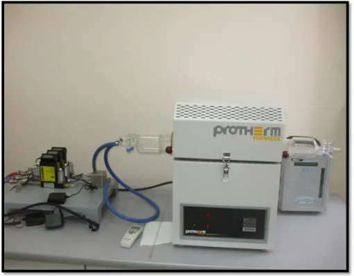
In the study, an n-Si wafer with (100) orientation and 1-10 cm resistivity is used. The wafer firstly degreased by boiling in trichloroethylene and cleaned by ultrasonically vibrating in acetone and methanol for 5 min. After each step, the wafer was washed with deinozed water. After cleaning procedures, the wafer is dried under nitrogen ambient. The n-Si semiconductor was put into the vacuum chamber. Au metal was evaporated at 10-6 Torr and n-Si/Au structure was annealed under nitrogen ambient for 3 min at 570 C to make high quality ohmic contact. The annealing furnace is shown in Fig 3.6.
3.MATERIALS AND METHODS
22
Fig 3.6 The annealing furnace used in the study 3.4.2. Deposition of Cr2O3 thin films
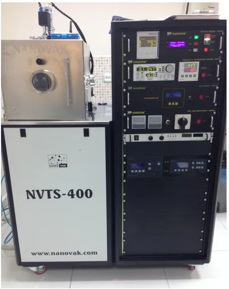
Cr2O3 thin films were growth on n-Si semiconductor and glasses by reactive sputtering technique using Nanovak NVTS 400 vacuum system. Cr metal was used as target and O2 was used as reactive gas. For all processes, firstly, pressure of the vaccum system was decreased at 10-6 Torr. Argon gas was send to system and the pressure was increased to 20 mTorr. The flow of the Argon gas was about 4 ccm. 80 W power was applied to high purity Cr target and 0,4 ccm oxygen was send to vacuum system to make reactive sputtering process. This process continued 10 minutes. The substrate
23
Fig 3.7. Nanovak NVTS 400 vaccum system
temperatures were 40, 150 and 250 °C during sputtering process. To increase crystallianity, Cr2O3 thin films were annealed at 500 °C for 30 minutes in air ambient.
3.4.3. Formation of front contact and measurements
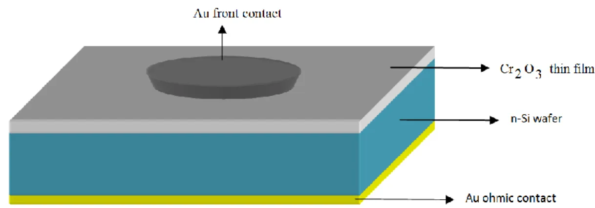
Au metal was evaporated to obtain front contact. The circular diameters of the Au contacts was about 1.5 mm. To make circular front contacts a shadow mask is used. The schematic diagram of Au/ Cr2O3/n-Si devices is given in Fig. 3.8.
3.MATERIALS AND METHODS
24
Fig 3.8. The cross section illustratioon of Au/ Cr2O3/n-Si diode
Electrical and photoelectrical characteristics of Au/Cr2O3/n-Si structures were analyzed using its current-voltage (I-V) and capacitance-voltage (C-V)measurements by the help of Keitley 2400 sourcemeter and Agilent 4294 A impedance analyzer at room temperature in dark, respectively. To see the effect of the light on the photoelectrical
Fig 3.9a. Current-voltage measurement system with Keithley 2400 sourcemeter and Oriel solar simulator
25
Fig 3.9b. Capacitance-voltage measurement system with Agilent 4294 A Impedance analyzer
properties of the device an Oriel 9600 solar simulator was used. Current-voltage (I-V) measurements were repeated under solar simulator between 40-100 mW/cm2 with 20 mW/cm2 intervals. The current-voltage and capacitance voltage measurement systems are given in Figure 3.9. Optical properties of the thin film on quartz were analyzed using Shimadzu 3600 Uv-vis-nir spectrophometer. The system is presented in figure 3.10.
3.MATERIALS AND METHODS
27 4. FINDINGS AND DISCUSSION
4.1. Introduction
In this chapter, optical properties of the Cr2O3 thin films grown at 40, 150 and 250 °C
are analyzed. After that, current-voltage properties of the Cr2O3/n-Si heterojucntions are
presented. The electrical and photoelectrical parameters of diode which has a best rectifying property (fabricated using thin film deposited at 250 °C) is examined.
4.2. Optical properties of Cr2O3 thin films on glasses
Optical properties of the Cr2O3 thin films were analyzed by means of UV-Vis
spectra. Fig. 4.1 shows the absorbance vs. wavelength plots of Cr2O3. As seen from the
figure, the absorbance of Cr2O3 thin films decreases sharply till 500-600 nm band then
decreases slightly till 1000 nm. After this value, the absorbance is nearly constant. It
means that the Cr2O3 thin film has small absorbance in infrared region. Furthermore, the
absorbance value of thin film decreases with increasing the grown temperature. The film deposited at 250 °C had the lowest absorbance values and the thin deposited at 40 °C had the highest absorbance values.
4.FINDINGS AND DISCUSSION
28
The optical band gap (Eg) of the Cr2O3 can be calculated through the equation
hvB(hvEg)m (4.1)
Where α is the absorption coefficient, B is a constant, h is the Plank constant, m
is ½ for direct band gap and 2 for indirect band gap. Cr2O3 has absorbance constant
higher than 104. Therefore, it can be said that Cr2O3 a direct band gap. In this study, the
band gap of sputtered Cr2O3 thin films were calculated by the help of (Ahv)2–hv plot
using equation 4.1 using. Figure 4.2 shows the (Ahv)2–hv sputtered Cr2O3 thin films on
glasses and The Eg of the Cr2O3 thin films were extracted as 2.99, 3.05 and 3.10 eV for
the film deposited at 40, 150 and 250 °C, respectively. The results show the strong
effect of substrate temperature on optical properties of Cr2O3 thin films.
Fig 4.2. (Ah)2-hplots of Cr2O3 thin film on a glass
4.3. Current-voltage properties of Cr2O3/n-Si heterojunctions
The current-voltage measurements of Cr2O3/n-Si heterojunctions are presented
in Fig.4.3. As it is seen from the figure, the diodes fabricated using the film deposited at 40 and 150 °C showed nearly ohmic properties and the device fabricated using the film deposited onto n-Si at 250 °C had an excellent rectification. These behaviors presented
29
Fig 4.3. lnI-V plots of Cr2O3/n-Si heterojunctions obtained various substrate
temperature
The perfect rectification for the heterojunction fabricated by deposition of Cr2O3
onto n-Si substrate at 250 °C may be because of the high quality of Cr2O3 thin film.
I-V relationship of a heterojunction for qV>>3kT (where q is the electron charge, V is the applied voltage, k is the Boltzmann constant and T is the absolute temperature) is owing to thermionic current. According to thermionic emission theory, the current-voltage relationship of a diode with a series resistance can be written as (Rhoderick and Williams 1988) nkT IR V q I I ( s) exp 0 (4.2)
where, RS is the series resistance, n is dimensionless ideality factor and I0 is the
saturation current which can be expressed
kT qΦ T AA I b exp 2 * 0 (4.3)
4.FINDINGS AND DISCUSSION
30
where A is the diode area, A* Richardson constant, b is the barrier height. The ideality
factor of a diode can be calculated from the slope of the linear region of the InI-V plot of the diode using the equation
) ln(I d dV kT q n (4.4)
The ideality factor of Au/Cr2O3/n-Si heterojunction formed by deposition of
Cr2O3 thin film was calculated as 1.29. Table 4.1 presents some electrical parameters of
the Au/Cr2O3/n-Si diode. The ideality factor of an ideal diode 1.01 when image force
lowering of the diode is taken into account. The ideality greater than this value shows a
non-ideal diode behavior. The non-ideal diode behavior of the Au/Cr2O3/n-Si may be
because of the effect on native oxide layer on n-Si semiconductor. It is known that except for special fabrications, a very thin native oxide layer occurs during fabrication process.
Another important electrical parameter of a diode is barrier height. The barrier height of the junction can be calculated using I0 value obtained from interception of
InI-V plot to I axis by the help of the equation
0 2 * ln I T AA q kT b (4.5)
The barrier heights of the device were calculated using saturation current value of Au/Cr2O3/n-Si by the help of the equation 4.5. The room temperature barrier height value of Au/Cr2O3/n-Si device determined as 0.761 eV. Sağlam et al fabricated 24
Au/n-Si Schottky barrier dots and reported the barrier height values between 0.789 and 0.819 eV (Sağlam, Cimilli et al. 2004). Therefore, Au/Cr2O3/n-Si diode has smaller barrier height value than conventional Au/n-Si MS diode. This result implies the strong effect of Cr2O3 thin film on the performance of the device.
Table 1. Some electrical parameters of Cr2O3/n-Si heterojunction at room temperature
lnI-V Norde C-V
n b (eV) F(V0) V0 b (eV) RS () b (eV) Nd (cm-3)
31
The curvature in the plot of Au/Cr2O3/n-Si heterojuncton fabricated using the
film deposited at 250 °C for high voltages is because strong effect of the series resistance on the current-voltage properties. The series resistance results from the
contact wires or bulk resistance of the Cr2O3 and n-Si semiconductors. The series
resistances of the Au/Cr2O3/n-Si structure were calculated by means of Norde functions
given below as
(* )2 T AA V I q kT V V F (4.6)where γ is the first integer greater than ideality factor and I(V) is the current obtained
from I–V measurements. The barrier height of device can be calculated using the minimum value of F vs. V plot using the equation
q kT V V F b 0 0) ( (4.7)
4.FINDINGS AND DISCUSSION
32
where F(V0) is the minimum F(V) value and V0 is the corresponding voltage value.
F(V)–V curve of Au/Cr2O3/n-Si heterojunction structure is depicted in Figure 4.4. The
series resistance of the device is determined through the relation
min qI n kT RS (4.8)Where Imin the corresponding current value at V0. The barrier height and the
series resistance values of the heterojunction are also depicted in table 4.1. As it is seen from the table, the series resistance and barrier height of the diode calculated as 9.169
k and 0.758 eV. The barrier height values of the diode obtained from both lnI-V and
F(V)-V plots are nearly same.
Furthermore, Figure 4.5 shows the current-voltage plots of Au/Cr2O3/n-Si
junction for various light intensities. As seen from the figure, light intensity has a strong effect on photoelectrical performance of the device. Some photoelectrical parameters including sensitivity to light at -3V (illuminated current/dark current), open circuit
Fig 4.5. lnI-V plots of Cr2O3/n-Si heterojunction in dark and various illumination
33
voltage and short circuit current values are given in table 2. As seen from the table, all photoelectrical parameters increase with the increase in light intensity. This property showed that the device had photodiode characteristics which are attributable to the formation of electron–hole pairs following optical absorption. Similar results have been reported for various metal oxide/silicon heterojunctions. For instance, Lee et al (2002) optimized ZnO/p-Si heterojunctions for photodiode applications. They deposited
n-ZnO thin films onto p-Si semiconductor at various temperatures in Ar/O2 ambient. They
reported that all structures had typical rectifying properties and maximum amount of photocurrent observed for n-ZnO/p-Si heterojunction when the ZnO film was deposited at 480 °C. The results showed that film growing conditions had strong effects on photoelectrical characteristics (Lee, Choi et al. 2002). Similarly, Alsayed et al (2015)
prepared CuNiO2 thin film by sol gel method onto p-Si substrate. They determined the
size of CuNiO2 nanoparticles as 115 nm and the band gap of the film as 2.4 eV. They
showed that the Al/p-Si/CuNiO2/Al heterojunction good rectification property in dark
and high photosensitivity value of 1.02 × 10³ under 100 mW/cm2(Elsayed, Çavaş et al.
2015).
Table 2. Photoelectrical parameters of Cr2O3/n-Si heterojunction
Light Intensity ISC (A) VOC (mV) Sensitivity to light (Times)
40 mW/cm2 3.79 10 83
60 mW/cm2 4.08 30 130
80 mW/cm2 4.34 30 190
100 mW/cm2 5.14 50 263
4.4. Capacitance-voltage properties of Au/Cr2O3/n-Si heterojunction
Capacitance-voltage measurements Au/Cr2O3/n-Si heterojunction for various
frequencies are depicted in Figure 4.6. As it is seen from the figure, capacitance value of the structure decreased for forward bias values with the increase in frequencies. It means that at sufficiently high frequencies, charge carriers at the interface can no longer follow the AC signal. This situation showed the strong effect of interface states to capacitance of the structure. The depletion region capacitance of a diode is given (Rhoderick and Williams 1988)
4.FINDINGS AND DISCUSSION 34
d N A s q V bi V 2 2 2 C 1 , (4.9)Where Vbi is the built-in potential, εS is the dielectric constant of the
semiconductor and Nd is the donor concentration. Nd was determined from the intercept
of a plot of C-2 as a function of V, and Vbi was determined from the gradient of this plot,
as shown in Fig. 6.7. The built-in potential, the barrier height and the donor
concentration of the Au/Cr2O3/n-Si diode were executed as 0.46 V, 0.718 eV and 7.434
x1014 cm-1, respectively. The barrier
35
Fig 4.7. C-2-V plot of Au/Cr2O3/n-Si heterojunction at 1 MHz
height value of the diode is in consistency with the value obtained from lnI-V and Norde plots. Erdogan and Güllü reported the carrier density , the built-in potential and the
barrier height of the Au/Cr2O3/p-Si MIS diode as 5.28 × 1014 cm−3, 0.73 V and 1.10 eV,
respectively. The obtained result for carrier density is very near to the one obtained in this study.
4.FINDINGS AND DISCUSSION
36
37 5. RESULTS AND SUGGESTION
In this study, three Cr2O3 thin films deposited on n-Si and glass substrates 40, 150 and
250 °C by reactive sputtering technique. During the sputtering process, high purity Cr
target was used as Cr source and O2 as reactive gas. All films were annealed at 500 °C
to improve the crystal quality of the films.
Optical properties of the Cr2O3 thin films on were analyzed by means of UV-Vis
spectra (Figs. 4.1 and 4.2). It was seen that the absorbance value of thin decreased with increase in deposition temperature. The film deposited at 250 °C had the lowest absorbance values and the thin deposited at 40 °C had the highest absorbance values. The band gap of sputtered Cr2O3 thin films were calculated by the help of (Ahv)2–hv
plot using equation 4.1 using UV-Vis data. The Eg of the Cr2O3 thin films were
extracted as 2.99, 3.05 and 3.10 eV for the film deposited at 40, 150 and 250 °C, respectively. The results showed the strong effect of substrate temperature on optical properties of Cr2O3 thin films.
The electrical properties of Cr2O3/n-Si heterojunctions were examined using
current-voltage measurements. The results showed that the diodes fabricated using the film deposited at 40 and 150 °C had nearly ohmic properties and the device fabricated using the film deposited onto n-Si at 250 °C had an excellent rectification. These
behaviors presented the substrate temperature effects of electrical properties of Cr2O3
/n-Si devices. The perfect rectification for the heterojunction fabricated by deposition of Cr2O3 onto n-Si substrate at 250 °C may be because of the high quality of Cr2O3 thin
film.
The electrical properties of Cr2O3/n-Si device fabricated by deposition of Cr2O3
onto n-Si substrate at 250 °C analyzed by means of both current voltage and capacitance-voltage measurements. It was seen that the device had 1.29 ideality factor,
0.761 eV barrier height and 9.169 k series resistance values at room temperature. The
barrier height value of the device calculated as 0.718 eV from C-V data. The ideality greater than unity was attributed the effects of native oxide layer on n-Si semiconductor and the series resistance of the device.
Furthermore, current-voltage measurements of Au/Cr2O3/n-Si junction were
taken under a solar simulator with AM1.5 Global filter for various light intensities. It was seen that light intensity had a strong effect on photoelectrical performance of the
5.RESULTS AND DISCUSSION
38
device. Some photoelectrical parameters including sensitivity to light at -3V (illuminated current/dark current), open circuit voltage and short circuit current values were given in table 4.2. As seen from the table, all photoelectrical parameters increase with the increase in light intensity. This property showed that the device had photodiode characteristics which are attributable to the formation of electron–hole pairs following optical absorption.
39 6. REFERENCES
Brockhouse, B. N. (1953). "Antiferromagnetic structure in Cr2O3." The Journal of Chemical Physics 21(5): 961-962.
Cheung, S. and N. Cheung (1986). "Extraction of Schottky diode parameters from forward current‐voltage characteristics." Applied Physics Letters 49(2): 85-87.
Elsayed, I., M. Çavaş, et al. (2015). "Photoconducting and photocapacitance properties of Al/p-CuNiO 2-on-p-Si isotype heterojunction photodiode." Journal of Alloys and Compounds
638: 166-171.
Erdoğan, İ. Y. and Ö. Güllü (2010). "Silicon MIS diodes with Cr 2 O 3 nanofilm: Optical, morphological/structural and electronic transport properties." Applied Surface Science
256(13): 4185-4191.
Green, M. A., K. Emery, et al. (2015). "Solar cell efficiency tables (Version 45)." Progress in photovoltaics: research and applications 23(1): 1-9.
Grove, W. R. (1852). "On the electro-chemical polarity of gases." Philosophical transactions of the Royal Society of London 142: 87-101.
Hao, R., J. Yuan, et al. (2006). "Fabrication and sensing behavior of Cr2O3 nanofibers via in situ gelation and electrospinning." Chemistry Letters 35(11): 1248-1249.
Kao, A., M. Doerner, et al. (1989). "Processing effects on the tribological characteristics of reactively sputtered chromium oxide (Cr2O3) overcoat films." Journal of Applied Physics 66(11): 5315-5321.
Kojima, A., K. Teshima, et al. (2009). "Organometal halide perovskites as visible-light sensitizers for photovoltaic cells." Journal of the American Chemical Society 131(17): 6050-6051. Lee, J., Y. Choi, et al. (2002). "Optimizing n-ZnO/p-Si heterojunctions for photodiode
applications." Thin Solid Films 403: 553-557.
Lin, F.-C., Y. Takao, et al. (1995). "Hydrogen-sensing mechanism of zinc oxide varistor gas sensors." Sensors and Actuators B: Chemical 25(1): 843-850.
Mostovoi, A., V. Brus, et al. (2014). "Charge-transport mechanisms in heterostructures based on TiO2: Cr2O3 thin films." Semiconductors 48(9): 1174-1177.
Mönch, W. (2014). "On the band-structure lineup at Schottky contacts and semiconductor heterostructures." Materials Science in Semiconductor Processing 28: 2-12.
Muller, R. and R. Zuleeg (1964). "Vapor‐Deposited, Thin‐Film Heterojunction Diodes." Journal of Applied Physics 35(5): 1550-1556.
Neamen, D. A. and B. Pevzner (2003). Semiconductor physics and devices: basic principles, McGraw-Hill New York.
Norde, H. (1979). "A modified forward I‐V plot for Schottky diodes with high series resistance." Journal of Applied Physics 50(7): 5052-5053.
O'regan, B. and M. Grätzel (1991). "A low-cost, high-efficiency solar cell based on dye-sensitized colloidal TiO2 films."
Ocak, Y. S., M. Kulakci, et al. (2011). "Analysis of electrical and photoelectrical properties of ZnO/p-InP heterojunction." Journal of Alloys and Compounds 509(23): 6631-6634. Rhoderick, E. H. and R. Williams (1988). Metal-semiconductor contacts, Clarendon Press
Oxford.
Stănoiu, A., C. Simion, et al. (2012). "NO 2 sensing properties of Cr 2 O 3 highlighted by work function investigations." Thin Solid Films 522: 395-400.
Yahia, I., M. Fadel, et al. (2011). "Analysis of current–voltage characteristics of Al/p-ZnGa 2 Se 4/n-Si nanocrystalline heterojunction diode." Journal of Alloys and Compounds
509(12): 4414-4419.
Yoo, J. and E. D. Wachsman (2006). "Potentiometric NOx sensing behavior of Cr2O3-based sensor and TPR of the sensor element." ECS Transactions 1(7): 173-184.
6. REFERENCES
40
Sağlam, M., F. Cimilli, et al. (2004). "Experimental determination of the laterally homogeneous barrier height of Au/n-Si Schottky barrier diodes." Physica B: Condensed Matter
Name : ALI A. ISSA Nationality : IRAQ
Birth Place : Duhok Date of Birth : 21.04.1980 Marital Status : Married
Foreign Language: Arabic, English
E-mail : [email protected] Education
Primary school : Sery Primary school intermediate school: Sery intermediate school Preparatory school : Sheladiz secondary school