GRAPHENE BASED OPTOELECTRONICS
IN THE VISIBLE SPECTRUM
A THESIS SUBMITTED TO
THE GRADUATE SCHOOL OF ENGINEERING AND SCIENCE OF BILKENT UNIVERSITY
IN PARTIAL FULFILLMENT OF THE REQUIREMENTS FOR THE DEGREE OF
DOCTOR OF PHILOSOPHY IN
PHYSICS
By
Emre Ozan Polat
January, 2015
ii
GRAPHENE BASED OPTOELECTRONICS IN THE VISIBLE SPECTRUM By Emre Ozan Polat
January, 2015
We certify that we have read this thesis and that in our opinion it is fully adequate, in scope and in quality, as a thesis for the degree of Doctor of Philosophy.
. Asst. Prof. Dr. Coşkun Kocabaş (Advisor)
. Prof. Dr. Bilal Tanatar
. Prof. Dr. Oğuz Gülseren
. Assoc. Prof. Dr. Emrah Özensoy
. Prof. Dr. Ahmet Oral
Approved for the Graduate School of Engineering and Science:
. Prof. Dr. Levent Onural Director of the Graduate School
iii
ABSTRACT
GRAPHENE BASED OPTOELECTRONICS
IN THE VISIBLE SPECTRUM
Emre Ozan Polat Ph.D. in Physics
Advisor: Asst. Prof. Dr. Coşkun Kocabaş January, 2015
Graphene, a two dimensional crystal of carbon atoms, emerges as a viable material for optoelectronics because of its electrically-tunable broadband optical properties. Optical response of graphene at visible and near infrared frequencies is defined by band electronic transitions. By electrical tuning of the Fermi energy, the band transitions can be blocked due to Pauli blocking. However, controlling inter-band transitions of graphene in the visible and near infrared wavelengths, has been an outstanding challenge. We developed a new device to control optical properties of graphene in the visible spectra. Our device relies on a graphene supercapacitor which includes two parallel graphene electrodes and electrolyte between them. Mutual gating between graphene electrodes enables us to fabricate optical modulators which can operate in the visible and near-infrared. Single layer graphene, however, has performance limits due to its small optical absorption defined by fundamental constants. We extend our method and we developed a new class of electrochromic devices using multilayer graphene. Fabricated devices undergo a reversible color change with the electrically controlled intercalation process. The electrical and optical characterizations of the electrochromic devices reveal the broadband optical modulation up to 55 per cent in the visible and near-infrared. Integration of semiconducting materials on unconventional substrates enables optoelectronic devices with new mechanical functionalities that cannot be achieved with wafer-based technologies. As a novel application, we demonstrate ultra thin electronic paper displays using the multilayer graphene as a reconfigurable optical medium. We anticipate that the developed devices would find wide range of applications in optoelectronics.
Keywords: Graphene, optical modulator, optoelectronics, supercapacitor, smart
iv
ÖZET
GÖRÜNÜR SPEKTRUMDA GRAFEN TABANLI
OPTOELEKTRONİK
Emre Ozan Polat Fizik, Doktora
Tez Yöneticisi: Yrd. Doç. Dr. Coşkun Kocabaş Ocak, 2015
İki boyutlu bir karbon kristali olan grafen, elektriksel olarak değiştirebilir geniş spektrum optik tepkisiyle optoelektronik için uyarlanabilir bir malzemedir. Görünür ve yakın kızılötesi spektrumda grafenin optik tepkisi bantlar arası geçişler tarafından belirlenir. Grafenin Fermi seviyesinin elektriksel olarak ayarlanması, bantlar arası geçişlerin engellenmesine neden olur. Fakat bantlar arası geçişlerin görünür ve yakın kızılötesi bölgede kontrol edebilmek büyük bir zorluktur. Grafenin optik özelliklerini kontrol etmek için yeni bir aygıt geliştirdik. Önerilen aygıt, superkapasitör yapısı kullanan parallel grafen elektrotlar ve bunların arasına hapsedilmiş sıvı elektrolitten oluşmaktadır. Grafen elektrotların karşılıklı elektriksel ayarlanması, görünür ve yakın kızılötesi spektrumda çalışabilen optik modülatörleri üretmemize olanak sunmaktadır. Fakat tek katmanlı grafenin temel sabitler tarafından belirlenen sınırlı optik soğurması nedeniyle performansı limitlidir. Kullandığımız tekniği geliştirerek çok katmanlı grafen tabanlı, yeni bir tür elektrokromik aygıt ürettik. Üretilen aygıtlar, elektriksel olarak kontrol edilen araya ekleme metoduyla, geri çevrilebilir renk değişimine uğramaktadır. Yapılan elektriksel ve optik karakterizasyonlar, çok katmanlı grafen tabanlı elektrokromik aygıtların görünür ve yakın kızılötesi bölgeyi kapsayan geniş bir spektrumda %55’e varan optik modulasyon sağladığını göstermiştir. Yarı iletken malzemelerin geleneksel olmayan alttaşlar üzerine entegrasyonu, yarı iletken alttaş kullanan teknolojilerle elde eldilemeyecek optoelektronik aygıtların üretimine olanak sunmaktadır. Yeni bir uygulama olarak; geliştirdiğimiz kağıt alttaşlar üzerine aktarılmış çok katmanlı grafeni ayarlanabilir optik ortam olarak kullanan, ultra ince ekran aygıtları sunuyoruz. Geliştirdiğimiz aygıtların optoelektronikte geniş bir uygulama alanı bulacağını umuyoruz.
Anahtar kelimeler: Grafen, optik modülator, optoelektronik, süperkapasitör,
v
Acknowledgement
I express my deepest gratitude to my advisor Asst. Prof. Dr. Coşkun Kocabaş for being such a supportive and helpful to me. I can safely say that this thesis would not be possible without his ground breaking ideas and deep knowledge. He always found a solution when I got stuck. He guided me perfectly. I really appreciate him for sharing his experince with me. I always feel that working with such a research-minded and friendly advisor made me a better researcher in all meanings.
I would like to thank Assoc. Prof. Dr. Emrah Özensoy and Prof. Dr. Bilal Tanatar. I strongly believe that, with the comments and reviews they made, my thesis became more complete and valuable. Having such a great scientists in my thesis committee was a great chance for me. Thank you again for sharing your experince with me. I would like to thank Prof. Dr. Oğuz Gülseren, Prof. Dr. Ahmet Oral for their precious questions and comments. They helped me to prepare a comprehensive study with their investigation for the physical background of my experimantal work.
I would like to thank to Prof. Dr. Alphan Sennaroğlu and Prof. Dr. Ömer Dağ for their collaborations. They created very important works as further applications of our study. I really learned much from you and it’s always an honour for me to collaborate with you.
I would like to express my appreciation for the financial support of TÜBİTAK. They supported us through the grants 112T686 and 113F278. This thesis would not be possible without the financial support of TÜBİTAK. The equipment and opportunities supplied by the grants contributed my research and enhanced my technical knowledge in a very efficient way. Thank you for supporting us.
I would like to thank to Murat Güre and Ergün Karaman. They are behind the scene heros of our research by keeping the Advanced Research Laboratory running. Thank you for your efforts and time.
I would like to thank to my collegues Osman Balcı, Nurbek Kakenov and Evgeniya Kovalska for their help and friendship during our research. Working with such a hardworking people always triggered me to do better research. I am sure you guys will achieve great successes during your lives. May the luck be with you!
vi
I would like to thank to my friends Edma Perini, Anita Dragonetti, Can Orhon, Arda Develioğlu, Semih Çakmakyapan, Selçuk Keskin, Hasan Özsoy, Tuna Dalcam, Aslı Çakan, Ertuğrul Karademir, Melike Gümüş, Zeynep Nilüfer Güven, Abdullah Kahraman, Abdullah Muti, Mehmet Can Kerse, Saniye Sinem Yılmaz and Ihor Pavlov. I am sure that the list is incomplete. Your perfect friendship keeps me delightful even in the darkest times. I am really glad to have you in my life. You are all amazing.
I dedicate this thesis to my family. They never let me feel alone from miles away during the times of my graduate school. They always couraged and supported me. They cathed me each time when I fall and made me carry on. I always feel safe and secure with their endless love. I am sure I will never have the fear of failing by knowing that such a strong bond is connecting them to me. You are the reason why I stand strong.
vii
Contents
1 Introduction ... 1
1.1 Outline ... 3
1.2 Graphene synthesis and transfer techniques ... 4
1.3 Electronic properties of graphene ... 13
1.4 Optical properties of graphene ... 26
2 Graphene Based Optical Modulators ... 32
2.1 Controlling the Optical Properties of Single Layer Graphene ... 33
2.2 Graphene Supercapacitors Working as Optical Modulators ... 35
2.3 Electro-optic Response... 39
2.4 Switching Performance ... 45
2.5 Device Schemes ... 46
3 Electrochromism in Multilayer Graphene... 50
3.1 Multilayer Graphene Electrodes ... 52
3.2 Graphene Based Electrochromic Devices ... 56
3.3 Operation Mechanism ... 58
3.4 Transmittance Modulation ... 61
3.5 Multi-pixel Displays ... 68
4 Graphene Based Paper Displays ... 71
4.1 Characterization of Multilayer Graphene on Paper ... 73
4.2 Electrically Controlled Colour Change ... 78
4.3 Ultra-thin Displays on Paper ... 81
5 Conclusions ... 84
viii
List of Figures
Figure 1.1: Techniques to obtain graphene. (a) Mechanically exfoliated graphene on oxidized Si dielectric surface. Reprinted from Novoselov, K.S., et al., Electric
field effect in atomically thin carbon films. Science, 2004. 306(5696): p.
666-669. Copyright © 2004, American Association for the Advancement of Science. (b) Atomic force microscope image taken from the surface of graphitized SiC substrate. Reprinted with permission from Kim, J., et al., Principle of direct van
der Waals epitaxy of single-crystalline films on epitaxial graphene. Nature
Communications, 2014. 5. Copyright © 2014, Nature Publishing Group. (c) Liquid phase graphene dispersions prepared by using various chemical agents. Reprinted with permission from Bourlinos, A.B., et al., Liquid-Phase
Exfoliation of Graphite Towards Solubilized Graphenes. Small, 2009. 5(16): p.
1841-1845. Copyright © 2014, Wiley-VCH Verlag GmbH & Co. KGaA, Weinheim. ... 5 Figure 1.2: Effects of copper surface morphology to graphene growth. (a) Optical microscope image of rough copper foil (Alfa Aesar foil (item #13382)). Deep scratches on the rough copper foil due to the rolling process, are clearly visible (b) Scanning electron microscopy (SEM) image of the rough copper surface. (c) The magnified SEM image of the rough copper foil surface. The growth was terminated after 10 sec. to obtain dispersed graphene flakes. (d) Optical microscope image of ultra-smooth copper foil (Mitsui mining and smelting co.
LTD., B1-SBS) and (e) SEM image of ultra smooth copper surface, after the
graphene growth. (f) Ultra smooth copper surfaces with graphene flakes. The density and shape of the graphene flakes are different on the rough and smooth foils. The averaged grain size of the smooth copper foil after the growth is around 200 µm. ... 8 Figure 1.3: Graphene flake formation at early stages of growth. (a,b) SEM images of the surface of the ultra smooth copper partially covered by graphene flakes. To achieve ~60µm flakes, methane gas was flushed into chamber for 5 seconds then left to cooling to room temperature. Smoothness of the surface and size of the grain boundaries of the copper are clearly visible. (c) AFM image showing the surface topography of full graphene layer on the ultra smooth copper foil. Graphene ripples, which are formed from the graphene flakes, are clearly seen. 9
ix
Figure 1.4: Graphene transfer by using PDMS stamping. (a,b) The nickel substrate is etched in FeCl3 solution to obtain the floating graphene on liquid surface.
(c)Then direct transfer to the rigid substrates by fishing out the graphen layer floating on the surface. (d-f) PDMS stamping to graphene holding nickel substrate and etching the metal foil in FeCl3 solution to obtain graphene on
PDMS. (g,h) Stamping the graphene holding PDMS to the dielectric surface to have conformal contact which results in the transfer of graphene layer on dielectric layer. Reprinted with permission from Kim, K.S., et al., Large-scale
pattern growth of graphene films for stretchable transparent electrodes. Nature,
2009. 457(7230): p. 706-710. Copyright (2009) Nature Publishing Group... 10
Figure 1.5: Transfer printing via photoresist drop casting. Reprinted with permission from Polat E.O., Kocabas C., Broadband optical modulators based on graphene supercapacitors. Nano Letters, 2012. 12(11): p. 5598-5602.). Copyright (2013) American Chemical Society ... 11
Figure 1.6: Raman spectroscopy of graphene. (a) Raman spectrum of the graphene as grown on gold surface. The inset shows the optical micrograph of the same area. (b) Raman spectrum of the graphene on SiO2/Si substrate. The inset shows the zoomed spectrum of the 2D peak and a Lorentzian fit. The width of the Lorentzian is around 37 cm-1. (c) Raman spectra of the graphene samples grown at a range of temperatures between 850 0C and 1050 0C. Reprinted with permission from Oznuluer, T., et al., Synthesis of graphene on gold. Applied Physics Letters, 2011. 98(18). Copyright © 2011 AIP Publishing LLC ... 12
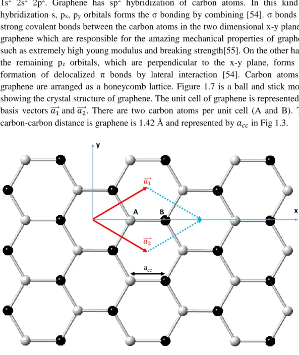
Figure 1.7: Crystal structure and basis vectors of graphene hexagonal lattice. ... 13
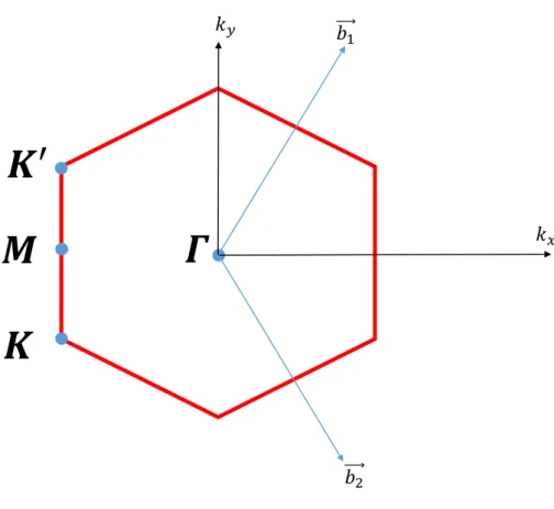
Figure 1.8: Brillouin zone and reciprocal basis vectors of graphene lattice. ... 15
Figure 1.9: Electronic band structure of graphene. ... 16
Figure 1.10: Linear dispersion of graphene at low energies. ... 17
Figure 1.11: Graphene based field effect transistors (FETs). (a) A schematic showing the back-gate FET with a graphene layer aligned between source and drain electrodes on the dielectric layer. (b) Three dimensional exploded view of a top-gate graphene based FET. Thin dielectric layer is deposited on graphene layer to apply the gate voltage from top of the device. Reprinted with permission from ‘‘Pince, E. and C. Kocabas, Investigation of high frequency performance limit of graphene field effect transistors’’. Applied Physics Letters, 2010. 97(17) Copyright (2010) American Institute of Physics. ... 19
x
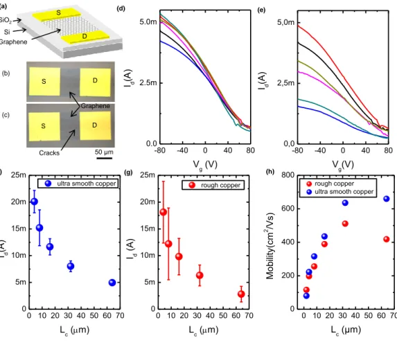
Figure 1.12 : Transport properties of fabricated graphene based transistors. (a) Schematic drawing of the fabricated graphene field effect transistor. The transistors use 100 nm thick SiO2 as a dielectric and highly doped Si as a back
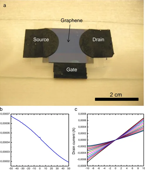
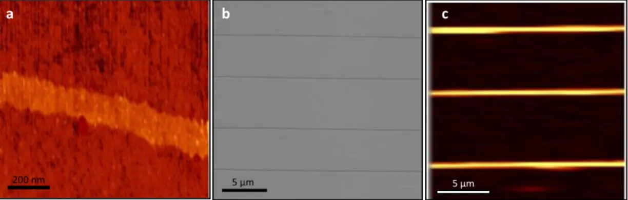
gate electrode. The source/drain electrodes are 50 nm thick gold. (b,c) Optical microscope images of the fabricated transistors based on the graphene grown on ultra-smooth copper foils, and rough copper foils respectively. The deep scrats on the copper foils results in visible cracks in transfered graphene. (d,e) Transfer curves of the transistors with a channel length of 64 µm, based on the graphene grown on the ultra smooth and rough copper foils, respectively. (f,g) The scaling of the drain current with the channel length of transistors. The scattered plot shows the averaged value of the drain current measured from 10 identical transistors. The error bars show the standart deviation of the drain current. The transistors based on rough copper foils show significantly larger variation in the drain current than the ones based on ultra shoorth copper foils. (h) The channel length scaling of the calculated field effect mobility of the transistors. ... 21 Figure 1.13: Macro scale graphene based FET and transport properties. (a) Photograph of the macro scale graphene based FET. Conductive carbon tapes are used as a contact electrodes. (b) Drain current vs. drain voltage characteristics of the device. (c) Modulation of the drain current with respect to applied gate voltage... 22 Figure 1.14: Fabrication steps of graphene ribbons via soft lithography ... 24 Figure 1.15: Structural characterizterization of fabricated graphene ribbons. (a) Atomic force microscope image of an individual ribbon. Ribbon height is measured as 2 nm on average. Due to the chemical process, the width of the ribbon varies between 150 nm to 200 nm in 1 µm ribbon length. b) Scanning electron microscope image of fabricated graphene ribbons on SiO2 surface. (c)
Raman mapping of submicron graphene ribbons on large area. ... 25 Figure 1.16: Interband conductivity of graphene with respect to wavelength. ... 27 Figure 1.17: Interband and intraband transitions in graphene. (a) Interband electronic transition on the Dirac cone of graphene. (b) For doped graphene when the Fermi energy is larger than half of the excitation energy, inter-band transitions are blocked due to Pauli blocking. (c) Intraband electronic transitions, which define the optical properties of graphene at far-infrared spectrum. Graphene behaves like a Drude metal. ... 29
xi
Figure 1.18: Electrical Control of Optical Plasmon Resonance with graphene. (a) Electrolyte gated graphene-gold-nanorod hybrid structure. A top electrolyte gate with ionic liquid is used to control the charge density and optical transitions on graphene. (b) A SEM image of the single gold nanorod covered by graphene. Reprinted with permission from Kim, J., et al., Electrical Control of Optical
Plasmon Resonance with Graphene. Nano Letters, 2012. 12(11): p. 5598-5602.
Copyright (2012) American Chemical Society ... 30 Figure 1.19: Controlling the plasma frequency of graphene by patterning graphene. (a) Patterning into graphene ribbons. Reprinted with permission from Ju, L., et al., Graphene plasmonics for tunable terahertz metamaterials. Nature Nanotechnology, 2011. 6(10): p. 630-634. Copyright © 2011 Nature Publishing Group (b) Making graphene/insulator stacks. Reprinted with permission from Yan, H.G., et al., Tunable infrared plasmonic devices using graphene/insulator
stacks. Nature Nanotechnology, 2012. 7(5): p. 330-334. Copyright © 2012
Nature Publishing Group (c,d) Graphene nano disks. Electrostatic doping of these pattered graphene introduces an additional control on the plasma frequency. Reprinted with permission from Fang, Z.Y., et al., Active Tunable
Absorption Enhancement with Graphene Nanodisk Arrays. Nano Letters, 2014.
14(1): p. 299-304. Copyright © 2013 American Chemical Society ... 31 Figure 2.1: Electronic properties of the graphene supercapacitor. (a) Schematic exploded view of the optically transparent double layer capacitor formed by two parallel graphene electrodes transfer-printed on quartz substrates and the electrolyte medium (5 mM TBA BF salt in DI water) between them. (b), (c) Schematic representation of the electronic band structure of the top and bottom graphene layers under a voltage bias. (d) Equivalent circuit of the supercapacitor. Superscript “T” and “B” represent the top and bottom electrodes, respectively. The arrows indicate the voltage-variable elements. (e), (f), The variation of the capacitance and resistance of the device as a function of bias voltage, respectively. ... 36 Figure 2.2: Comparison of electrostatic capacitance and quantum capacitance.(a) Electrostatic capacitance of the electrical double layer of aqueous electrolyte (5mM of TBA BF4 in DI water) measured using gold electrodes. (b) Calculated capacitance of the top (Ct) and bottom (Cb) graphene electrodes (Dirac point of
the bottom graphene is shifted by 0.7 V), electrostatic double layer (averaged value of 30 µF/cm2 calculated from the previous measurement) and the equivalent capacitance (Ceq) of the super capacitor. Cq represents the total
quantum capacitance of the graphene electrodes. The difference between Cq and
Ceq shows the contribution of the double layer capacitance. At low carrier
concentration, the capacitance is limited by the quantum capacitance and at high concentrations, the contribution of double layer capacitance flattens the total capacitance. ... 38 Figure 2.3: Optical absorption of graphene electrodes in graphene supercapacitor. . 38
xii
Figure 2.4: Electro-optic characterization of graphene supercapacitor based optical modulators. (a) Picture of the fabricated graphene supercapacitor. The black regions are carbon electrodes that are used to make electrical contact to graphene. (b) The normalized change of the transmission of the capacitor plotted against wavelength and bias voltage. (c) The variation of the normalized change of the transmission versus the wavelength for various bias voltages. (d) Fermi energy (scattered plot) extracted from the electro-optical response of the capacitor and measured capacitance (solid red curve). Both Fermi energy and the capacitance show ~𝑛 dependence. ... 40 Figure 2.5: Near-infrared respond of graphene supercapacitor based optical modulators. Modulation of the normalized transmission of graphene supercapacitor at near-infrared regime. The Fermi energy of undoped graphene is estimated as 250 meV. ... 41 Figure 2.6: Raman spectroscopy of graphene supercapacitor based optical modulators. (a) Intensity map of Raman scattering of the graphene electrode as a function of Raman shift and applied voltage. The labels indicated the D, G and 2D Raman peaks of graphene. (b,c) Variation of Raman frequency and intensity of 2D and G bands as a function of bias voltage. (d) Raman spectra of defected graphene electrodes after application of bias voltages larger than the electrochemical window of the electrolyte. ... 42 Figure 2.7: Ionic liquid performance in the graphene supercapacitor. (a) Normalized change of the transmission of a graphene supercapacitor that uses ionic liquid as an electrolyte for bias voltage in the range of -5V to 0 V. (b) The cut-off energy (2Ef) as a function of bias voltage. (c) Illustration of gate-induced
change of Fermi energy for top and bottom graphene for different bias voltage. ... 43 Figure 2.8: Electrical properties of graphene supercapacitor with ionic liquid electrolyte (a) The measured capacitance and resistance of graphene supercapacitor with ionic liquid electrolyte. The scattered plot shows the extracted Fermi energy. The deviation of the measured capacitance from 𝑛 dependence is likely due to the large contribution of capacitance of the ionic double layer. (b) The measured capacitance at frequency of 20Hz for 1cm2 capacitor with gold electrodes and the ionic liquid electrolyte. The capacitance is significantly less than the aqueous electrolyte due to low ionic mobility of ions in the ionic liquid. ... 44 Figure 2.9: Switching performance of graphene optical modulators. (a) Normalized transmittance of the capacitor at bias voltages of -2 V and -3 V. The vertical red line indicated the working wavelength (635 nm) (b) Time trace of the bias voltage applied between graphene electrodes. (c) Time trace of the normalized transmittance. (d) The variation of the total capacitance as a function of frequency at a bias voltage of 0V. ... 45
xiii
Figure 2.10: Various device schemes to increase the modulation efficiency. Graphene supercapacitors using (a) single layer and (b) multilayer graphene electrodes, (c) Reflection type graphene optical modulator. (d) Normalized transmittance of the graphene supercapacitor with multilayer graphene electrodes. (f), Normalized reflectance of the graphene supercapacitor with a reflecting surface. ... 46 Figure 2.11: Single and multilayer graphene based optical modulators. (a) Broadband absorbance of multi layer graphene on glass substrate (The red curve). The black curve shows the background signal. (b) Photographs of large area single layer graphene and multilayer graphene transfer-printed on glass substrates. (c) Raman spectra of single layer graphene (d) Raman spectra of multi layer graphene. ... 47 Figure 2.12: Polarization independent operation of graphene based optical modulators. (a) Schematic diagram of the graphene supercapacitor and the polarization of light with respect to the device geometry. Normalized transmittance of the supercapacitor for vertical (b) and horizontal (c) polarizations. The device shows polarization independent operation. ... 48 Figure 2.13: Graphene supercapacitors using flexible substrates. (a) Single layer graphene transfer printed on a flexible PET substrate. (b) Normalized transmission of the flexible graphene supercapacitor for various bias voltages. 49 Figure 3.1: Synthesis and characterization of multilayer graphene on flexible substrates. (a) Transfer printing of large area multilayer graphene on flexible PVC substrates by lamination process. Multilayer graphene electrodes were synthesized on metal foils (copper or nickel), then 75 µm thick PVC film was laminated on graphene coated side. (b) Etching the metal foils yields flexible multilayer graphene electrodes on the PVC support. (c) Photograph showing the flexible multilayer graphene electrodes. (d) Raman spectra of the samples synthesized on copper and nickel foils. (e) Optical transmittance spectra of the MLG electrodes using grown on nickel at different temperatures. (f) Variation of the sheet resistance (blue curve) and optical absorption (red curve) of MLG electrodes with the layer number. ... 52 Figure 3.2: Multilayer graphene on metal and polymer substrates. (a,b) Photographs of the bare nickel foil and graphene grown on nickel foil respectively. (c) Photograph of graphene on PVC substrate. ... 53 Figure 3.3: Resistivity and transmittance of various thickness graphene samples.
(a-c) Transfer line measurements for three different MLG. The slope yields the sheet resistance of the electrodes. The sheet resistance varies between 13 Ω/sq to 1300 Ω/sq. (d) Optical transmission spectra of the MLG electrodes used for transfer line measurements. ... 54 Figure 3.4: Bending test for the graphene electrodes. (a,b) photographs of the MLG electrodes on flexible PVC substrates. (c) Variation of resistance of MLG electrode as the electrode is deformed. (d) The histogram of the resistance. .... 55
xiv
Figure 3.5: Graphene electrochromic devices. : (a) Exploded-view illustration of the graphene electrochromic device. The device is formed by attaching two graphene coated PVC substrates face to face and imposing ionic liquid in the gap separating the graphene electrodes. (b,c) Photographs of the devices under applied bias voltages of 0 V and 5 V, respectively. The image of Bilkent University logo [copyright permission from I.D. Bilkent University] appears at 5 V. Demonstrated device is composed of two multilayer graphene electrodes synthesized at 925 0C each having ~78 layers. (d) Transmittance spectra of the device under applied voltage between 0 V to 5 V. e, Variation of the transmittance (at 800 nm) with the applied voltage. (f) Variation of the Raman spectra of graphene electrodes under the applied voltage. (g-i) Schematic representation of the proposed operating regimes, i.e. neutral, charge accumulation, and intercalation, respectively. ... 56 Figure 3.6: Mechanism for the electrochromism in multilayer graphene. Schematic representation of the proposed operating regimes, (a) neutral, (b) charge accumulation, and (c) intercalation, respectively. ... 58 Figure 3.7: The variation of the optical transmittance of the device at +4 V. The intercalation process starts from the edge of the sample and propagates along the device. ... 59 Figure 3.8: Switching performance of the graphene electrochromic device. Time trace of the (a) percentage transmittance and (b) charging current. ... 60 Figure 3.9: Effect of thickness and quality of graphene on the device performance. Transmittance spectra (under applied voltage ranging from 0 V to 5 V) of electrochromic devices using various thicknesses of MLG. Devices shown in (a-c) use MLG grown on copper foils while devices shown in (d-f) use MLG grown on nickel foils, respectively. The inset shows the estimated number of graphene layers. The color bar shows the applied voltage... 62 Figure 3.10: Calculated optical transmission of MLG plotted against the number of layers. T= (1-α)N, where T is the transmission, α is the absorption of single layer which is around 2.3 % and N is the number of graphene layers. ... 63 Figure 3.11: Tranmittance modulation of graphene electrochromic devices. Variation of the transmittance (at 800 nm) of ECD using MLG grown on (a) copper and (b) nickel foils, respectively. (c) Maximum optical modulation plotted against the estimated number of graphene layers. ... 64 Figure 3.12: Charging and discharging characteristics of graphene electrochromic devices. (a) Schematic illustration of the experimental setup used for the simultaneous electrical and optical characterization of the graphene electrochromic devices. (b) Current-voltage and c, transmittance-voltage curves at 635 nm at a scan rate of 0.5 V/s. (d) Current-voltage and (e) transmittance-voltage for different scan rates. ... 64 Figure 3.13: Scan rate characteristics of graphene electrochromic devices. (a) Maximum current and (b) maximum optical modulation versus the scan rate. . 65
xv
Figure 3.14: Optical switching characteristics of the device at 635 nm. (a) Transmittance modulation of the graphene electrochromic device with respect to time. Time variation of (b) transmittance and (c) charging current for a single switching cycle. The extracted RC time constants of the electrochromic device (3.5 seconds for charging and 0.25 seconds for discharging respectively) are illustrated on the single switching cycle with intervals defined by the red bars.66 Figure 3.15: Stability test for graphene electrochromic devices. Long term stability of the transmittance in the (a) on-state (at 5 V) and (b) off-state (0 V). (c,d) The histogram of the transmittance in the on- and off-state. ... 67 Figure 3.16: Multi-pixel display device. (a) Schematic illustration of the multi-pixel display device consisting of 3 x 3 arrays of flexible electrochromic device. (b) Photograph of the fabricated flexible multi-pixel device. (c) Photographs of the device under various bias voltages that generate chessboard pattern. (d) Photographs of the device under 5 V bias voltage with different reconfigurable patterns. ... 69 Figure 3.17: Graphene based reflective electrochromic devices. (a) Exploded-view schematic illustration of the reflective graphene-electrochromic device consisting of gold and multilayer graphene electrodes. (b,c) Photograph of the fabricated device at 0 V and 5 V applied voltage, respectively. (d) Modulation of the reflectance spectra of the devices under various applied voltages. (e) Photograph of the flexible multi-pixel reflective device. (f,g) Photographs of the reflective device under bias voltage of 0 V and 5 V that generate chessboard pattern. ... 70 Figure 4.1: Scanning electron micrograph of paper surface coated with
ML-graphene. ... 73 Figure 4.2: Multilayer graphene on paper. (a) Photograph of multilayer graphene transferred on printing paper. (b) Dark field optical micrograph of MLG on paper. (c,d) Scanning electron microscope of the cross section and edge of graphene layer on paper. The bright area is due to electrostatic charging of the paper. The RMS surface roughness is around 3 µm. ... 74 Figure 4.3: Transferring ML-graphene on paper. (a) Schematic drawing of the transfer process. Due to the hydrophobic nature of the graphene surface, ML-graphene stay on the water surface. (b) Photograph taken during the transfer process. ... 75 Figure 4.4: Scattering cross section and resistance measurements. (a) Scattering cross section (at 650 nm) of bare paper surface (red curve) and graphene coated surface (blue curve). The black curve shows the Lambartian cosine model. The inset shows the configuration. (b) Resistance of graphene for various folding configurations. ... 75 Figure 4.5: Angular dependent normalized scattering cross section of paper coated with ML-graphene grown at different temperature. ... 76 Figure 4.6: Variation of the resistance of ML-graphene as we continuously fold the paper substrate. ... 77
xvi
Figure 4.7: Continuos device operation during folding. ... 77 Figure 4.8: Optoelectronic property of ML-graphene on paper. (a) Schematic representation of the graphene based electronic paper. (b,c) Photographs of the fabricated e-paper at various bias voltages. (d,e) Optical microscope image of the edge of ML-graphene at various bias voltages... 78 Figure 4.9: Electrical control of optical properties. (a) Scattering cross section (at 650 nm) from the ML-graphene measured at bias voltages between 0 V to 5 V. (b) Spectrum of the scattered light from the ML-graphene at various bias voltages. (c) Evolution of the Raman spectra of ML-graphene with the bias voltage. ... 79 Figure 4.10: Switching characteristics of the device. (a) Scattering intensity against time, (b) current versus time behaviour during switching between on and off states. ... 80 Figure 4.11: Controlling colour of ML-graphene on normal printing paper. (a) In the off-state of the device graphene looks reflective. Conductive carbon tapes are used as the contact electrodes. (b) Applying 4V bias voltage yields the reversible color change of multilayer graphene on normal printing paper. ... 80 Figure 4.12: Multipixel e-paper display. (a) Schematic representation of multipixel paper display using 3x3 array of patterned graphene electrodes. The width and the length of graphene electrodes are 7 mm and 3 cm, respectively. (b) Photograph of the reconfigurable pattern on paper using passive matrix addressing at various voltage configurations. ... 81 Figure 4.13: Demonstration of colour principle. (a) Schematic representation of colour e-paper formed by printing halftone colour toner on paper sandwiched between two ML-graphene electrodes. (b) Optical microscope image of colour toner dots printed on paper. (c,d) Photograph of the working device at 0 and 5 V bias voltage. ... 82 Figure 4.14: Diposable the e-paper. (a) A photograph of a burning device. The paper substrate burns very fast however, the ML-graphene layer does not burn. (b) The ashes of the device. The reaming graphene layer on the paper ash is visible. ... 83
1
Chapter 1
Introduction
Graphene is a two dimensional crystal of carbon atoms arranged in a honeycomb lattice. This atomically thin carbon crystal is a basic building block of other carbon allotropes such as one dimensional carbon nanotube, zero dimensional fullerene and three dimensional graphite [1]. Starting with the first observation of strong ambipolar electric field effect in the graphitic films [2] by Andre Geim and Kostya Novoselov, there has been a tremendous amount of effort from scientist and researchers to explore and enhance the electronic properties of graphene in the last decade. Groundbreaking discoveries such as experimental observation of the half integer quantum hall effect [3, 4], constant minimum conductivity in vicinity of charge carriers [5], ballistic transport at room temperature [1] and Klein paradox [6] open a gate through the graphene based basic science and fabrication of future electronic devices.
Graphene also has some unusual optical properties. Even if it is a one-atom-thick material, it can be seen on certain dielectric layer thickness [7] which provides an easy optical characterization even with the optical microscope. The main optical properties of the graphene such as the transmittance and reflectance are defined by the fine structure constant [8]. Furthermore, graphene has a gate tunable broad optical response [9] and one can simply control the absorption mechanism of graphene via electrostatic doping [10]. That intriguing optical properties make the graphene valuable for optical investigation and photonic devices.
The aim of this thesis is to develop the graphene based optoelectronic devices working in visible spectra. We will present active optical devices using the unconventional electronic and optical properties of this two dimensional carbon crystal.
After giving the fundamentals of graphene electronics and optics, we will demonstrate an efficient gating scheme using graphene supercapacitors which controls the absorption mechanism of graphene by Pauli blocking of interband
2
transitions. By using this gating scheme we will perform some electro-optic characterizations in visible and infrared spectra revealing the light-matter interaction in graphene in a broad spectrum. To show the promises of the method, we will also demonstrate the applications such as graphene based flexible electrochromic devices and graphene based e-papers by further expanding our investigation into multilayer graphene.
3
1.1 Outline
This thesis presents the new gating scheme which allows the graphene based optical devices to operate in visible spectra. Furthermore, it demonstrates the first practical graphene devices working in visible spectra using the presented gating scheme.
In chapter 1 we will provide the fundamental knowledge about graphene synthesis and transfer methods. We will briefly explain the methods that we used to obtain graphene layers and compare them to the previously used ones. Then, we will give the theroretical background for the electronic and optical properties of graphene which is required for the better understanding of the working mechanism and characterization of our fabricated graphene based devices.
Chapter 2 presents ‘‘controlling optical properties of single layer graphene’’ which contains the brief explanation about the physical mechanism and electro-optic characterization steps of the transparent graphene supercapacitors working as an optical modulators.
Chapter 3 includes the ‘‘optical properties of multilayer graphene’’ which demonstrate the first application of active reversible color change in the flexible multilayer graphene electrodes. In this chapter we will introduce the multilayer graphene as a new class of electrochromic material having key parameters for high contrastand broadband operation by using our proposed gating scheme.
Chapter 4 is introduces an interesting practical application. ‘‘Graphene on paper’’. In this chapter we demonstrate electronic paper display using graphene transferred on
printing paper as the reconfigurable optical medium. The presented graphene based
ultrathin electronic paper display provides large optical contrast in the visible spectra with fast response speed.
Chapter 5 inludes the conclusion of our studies and provides an outlook of the presented devices.
4
1.2 Graphene synthesis and transfer techniques
In order to study the physical properties of the graphene one should isolate the two dimensional graphene layer. This is a challenging procedure due to the atomic thickness of graphene. However during the last decade several consistent methods have been developed to obtain the one-atom-thick single layer graphene which was previously thought to be instable. In the followings we will give a short review by explaining the advantages and disadvantages of these methods.
Mechanical exfoliation from bulk graphite [2] (also known as scotch-tape method) yields a non uniform thickness carbon film having fragments of different number of graphene layers. That makes the identification of single graphene layers difficult over the transferred substrate, yet it is still a simple method to study the fundamental electronic properties of graphene over very limited area (Fig. 1.1 (a)). This method gives the highest carrier mobilities (200,000 cm2 V-1 s-1) in graphene based field effect transistors [11, 12].
Graphitization of SiC planes by annealing is another prominent method to obtain the two dimensional graphene. Epitaxial growth of graphene on SiC substrates (Fig. 1.1 (b)) and the promises of the method such as patterning the as grown graphene into the quantum confined structures was demonstrated [13]. By using this method, growth of relatively large area graphene samples are possible and devices using epitaxially grown graphene on SiC can operate in high frequency regime [14]. On the other hand, some handicaps such as high cost of the SiC substrates and requirement of ultra-high vacuum chambers still remain as disadvantages in the technique.
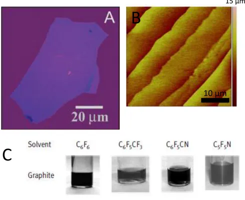
Isolating graphene layers chemically from the bulk graphite is an alternative method in which the intercalation of atoms or molecules through the graphite [15] yields the seperation of graphene layers. However partial separation of the bulk graphite yields a dispersion that contains variety of graphene fragments and graphitic films [16]. To overcome this non-uniformity of the resulting graphene layers, chemical reduction of graphene oxide [17] and chemically functionalized graphene [18] were introduced (Fig. 1.1 (c)). However since these materials are suffer from low conductivity, achieving the conductivity order of the pristine graphene with this method is a handicap to date.
5
Figure 1.1: Techniques to obtain graphene. (a) Mechanically exfoliated graphene
on oxidized Si dielectric surface. Reprinted with permission from Novoselov, K.S., et al., Electric field effect in atomically thin carbon films. Science, 2004. 306(5696): p. 666-669. Copyright © 2004, American Association for the Advancement of Science. (b) Atomic force microscope image taken from the surface of graphitized SiC substrate. Reprinted with permission from Kim, J., et al., Principle of direct van
der Waals epitaxy of single-crystalline films on epitaxial graphene. Nature
Communications, 2014. 5. Copyright © 2014, Nature Publishing Group. (c) Liquid phase graphene dispersions prepared by using various chemical agents. Reprinted with permission from Bourlinos, A.B., et al., Liquid-Phase Exfoliation of Graphite
Towards Solubilized Graphenes. Small, 2009. 5(16): p. 1841-1845. Copyright ©
2014, Wiley-VCH Verlag GmbH & Co. KGaA, Weinheim.
Today one of the most commonly used synthesis technique in graphene science is chemical vapor deposition (CVD). The advantages of the CVD synthesis over other techniques are scalability to large area, being low cost and effortless, and the consistent quality of the resulting graphene layers. Very large area CVD synthesized graphene samples were demonstrated and used as transparent electrodes in functional touch screen panel [19]. To form a graphene layer via CVD synthesis, a catalyst substrate is needed for the decomposition of carbon atoms from the carbon feedstock gas flowing through the CVD chamber. Nickel and copper substrates are frequently used as catalyst substrates, however usage of transition metals such as, Ir [20], Au [21], Ru [22], Pd [23] in CVD synthesis have also been demonstrated. The transport properties of the CVD synthesized graphene films are not superior compared to the mechanically exfoliated ones. This is due to the polycrystalline structure of the metal
C
B
10 µm 15 µm
6
substrates on which the graphene forms. However with the efficient controls of the gases flowing through the CVD chamber, large area single crystal graphene has already been reported [24]. For large area electronic applications, high quality samples with uniform transport properties are essential. Many breakthrough improvements on the quality of resulting graphene films in CVD synthesis have been reported [19, 25, 26]. Because of the low solubility limit of carbon in copper, graphene growth procedure is self-limited on copper substrates [25]. That property of copper provides the advantage of straightforward synthesis of single layer graphene. Copper foils are low cost and scalable substrates for graphene growth. The surface quality of the copper foils and the transfer printing process determine the performance and reliability of the graphene transistors. Commercially available copper foils, however, have very rough surfaces due to the rolling process. Deep scratches on the rough copper foil due to the rolling process, yield detrimental effects especially during the transfer printing process.
Previous works have showed that the morphology of the copper surface is one of the key parameters to have better quality graphene films [27]. To achieve the full surface coverage of the high quality graphene film; impurities, defects, grain boundaries and other surface features that can serve as a nucleation seed should be carefully engineered [27]. For that purpose, variety of techniques for smoothing the copper surfaces have been reported. Luo et al. [28] used standard electropolishing technique to smooth the copper surfaces. Their Raman spectroscopy investigation implied better quality graphene film with high surface coverage compared to the unpolished copper samples [28]. Similar electrochemical polishing technique was used in the work by Yan. et al [29]. Together with the high pressure annealing, they produced hexagonal single crystal graphene domains nearly 2mm in size [29]. Alternatively, melted copper surfaces were also used to form these single crystal hexagonal graphene flakes in previous works [30, 31]. Apart from these techniques, Vlassiouk et al.[32] reported the role of hydrogen gas as a surface activator and etchant. The shape and size of the single crystal graphene domains can be controlled precisely by adjusting the partial pressure of hydrogen gas [32]. In addition, Robertson et al. [33] showed the formation of few layer, single crystal, graphene flakes by changing the growth conditions.
Another prominent technique to form a smooth copper surface is the thin film deposition of copper on rigid substrates[34]. Howsare et al. [34] showed that adding a barrier layer between the deposited Cu and Si interface can further increase the quality of the graphene film by suppressing the interdiffusion between these layers. Moreover, Zhao et al. [35] investigated the effect of single crystal copper substrates on growth of the graphene layers. They reported the atomic structure of the graphene film and the grain orientations shows different properties going in different lattice directions [35].
7
It is known that the quality of the copper surface directly effects the transport properties of the resulting graphene layer [36]. Orofeo et al. [36] demonstrated the hole mobility of the graphene grown on the Cu film is nearly 10 times greater than that of the graphene grown on the Cu foil by chemical vapor deposition. In addition to surface morphology, crystallography of copper substrate also plays a cruical role in the formation of the graphene film [37]. Wood et al. [37] reported that, because of the carbon’s higher diffusion rates at (111) surface, it is more likely to have monolayer graphene on that surface compared to other surfaces
In our experiments we used the high quality single layer graphene on commercially available ultra-smooth copper foils. In the industry, copper foils have been used as negative electrodes for lithium-ion batteries. For these applications surface quality plays a critical role in the performance of the batteries. Recent progress of large scale production of smooth copper foils can also provide opportunities to improve performance of graphene transistors.
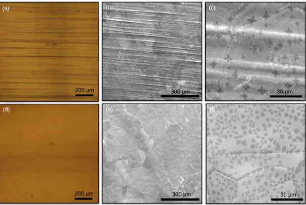
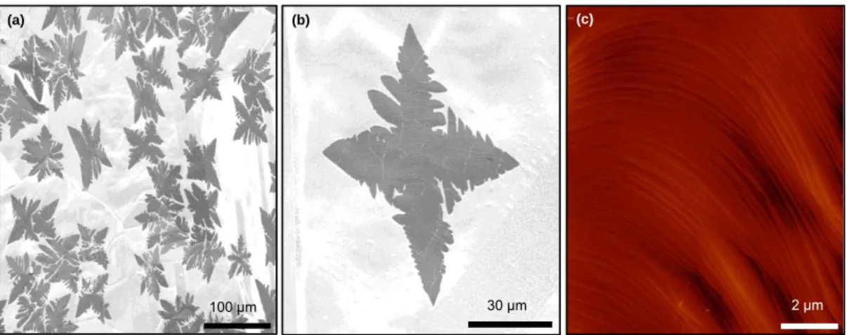
We used relatively rough Alfa Aesar foil (item #13382) which is commonly used for CVD graphene growth (Fig. 1.2 (a-c)) and commercially available ultra-smooth surface copper foils (Mitsui mining and smelting co., LTD, B1-SBS) (Fig. 1.2 (d-f)). To investigate the effect of the surface roughness to the quality of the graphene layer, both the ultra smooth copper and the rough copper foils were placed in the same growth chamber to be exposed to same growth conditions. We also investigated the surface topography of the ultra-smooth copper foils with SEM and AFM. The ratio of the partial pressure of hydrogen and methane gases define the growth rate and shape of the graphene flakes. By sending the methane gas into the chamber with different intervals we obtain both the graphene flakes (Fig 1.3(a), (b)) and full coverage graphene film (Fig. 1.3 (c)) on the ultra-smooth copper foils. Figure 1.3 (a) shows the SEM images of copper surface partially covered by graphene flakes. The surface roughness of the copper is around 100nm. However, after the growth, graphene flakes form ripples (Fig. 1.3 (c)) likely because of physical instability of perfectly flat graphene layer [38-41].
8
Figure 1.2: Effects of copper surface morphology to graphene growth. (a) Optical microscope image of rough copper foil (Alfa Aesar foil (item #13382)). Deep scratches on the rough copper foil due to the rolling process, are clearly visible (b) Scanning electron microscopy (SEM) image of the rough copper surface. (c) The magnified SEM image of the rough copper foil surface. The growth was terminated after 10 sec. to obtain dispersed graphene flakes. (d) Optical microscope image of ultra-smooth copper foil (Mitsui mining and smelting co. LTD., B1-SBS) and (e) SEM image of ultra smooth copper surface, after the graphene growth. (f) Ultra smooth copper surfaces with graphene flakes. The density and shape of the graphene flakes are different on the rough and smooth foils. The averaged grain size of the smooth copper foil after the growth is around 200 µm.
(e) (b) (c) (a) 200 µm (a) (d) 200 µm 300 µm (b) 300 µm (e) 30 µm (c) (f) 30 µm
9
Figure 1.3: Graphene flake formation at early stages of growth. (a,b) SEM
images of the surface of the ultra smooth copper partially covered by graphene flakes. To achieve ~60µm flakes, methane gas was flushed into chamber for 5 seconds then left to cooling to room temperature. Smoothness of the surface and size of the grain boundaries of the copper are clearly visible. (c) AFM image showing the surface topography of full graphene layer on the ultra smooth copper foil. Graphene ripples, which are formed from the graphene flakes, are clearly seen.
Since electronic and optical properties of the graphene can’t be examined on conducting metal substrates, the transfer printing of graphene layers to insulating substrate are essential in CVD synthesis. There are two commonly used transfer printing method for CVD synthesized graphene; namely the polymer-assisted transfer printing and roll-to-roll transfer printing [42].
PDMS (polydimethylsiloxane) is a silicon elastomer which is generally used for molding of microchannels [43] or as an optical mask for soft lithography [44]. Due to the low surface energy [45] and the hydrophobic nature of the PDMS [46] one can easily attach and retrieve graphene on PDMS surface (Figure 1.4). By using the PDMS stamping method, dry transfer of large area patterned multilayer graphene samples has been demonstrated [47]. However, formation of cracks along the graphene layer during the stamping and removal of PDMS to the insulator surfaces breaks up the uniformity of the transfer printed graphene layer by using PDMS stamping method. 2 µm (c) 100 µm (a) 30 µm (b)
10
Figure 1.4: Graphene transfer by using PDMS stamping. (a,b) The nickel
substrate is etched in FeCl3 solution to obtain the floating graphene on liquid surface.
(c)Then direct transfer to the rigid substrates by fishing out the graphen layer floating on the surface. (d-f) PDMS stamping to graphene holding nickel substrate and etching the metal foil in FeCl3 solution to obtain graphene on PDMS. (g,h) Stamping
the graphene holding PDMS to the dielectric surface to have conformal contact which results in the transfer of graphene layer on dielectric layer. Reprinted with permission from Kim, K.S., et al., Large-scale pattern growth of graphene films for
stretchable transparent electrodes. Nature, 2009. 457(7230): p. 706-710. Copyright
(2009) Nature Publishing Group.
Another polymer-assisted graphene transfer printing method is using PMMA (polymethyl methacrylate). Being highly conformal and having low density compared to PDMS, PMMA is able cover and embed the surface structures when baked [48]. Basically, spin coating of PMMA and etching the graphene holding metal substrates results in graphene holding PMMA [49]. Putting the graphene holding PMMA on the target substrate and removing the PMMA with acetone yields the graphene on desired target substrate. Disadvantages of the method can be mentioned as the unsuccessful removal of the whole PMMA along the graphene layer which affects the transports measurements by introducing scattering points [50]. In addition, PMMA transfer method could remain random cracks on the surface. However it has been reported that applying another layer of PMMA before the removal of PMMA could prevent the formation of cracks during the transfer [51].
11
To obtain a non-residual and crack-free transfer of CVD synthesized graphene layers we developed the photoresist drop casting method (Fig. 1.5). In this method, we poured thick droplets of photoresist (S1813) on graphene grown smooth copper surfaces and waited overnight at 70 0C. After a photoresist layer was hardened on smooth copper surfaces, they were immersed into nitric acid solution (~%22) for non-residual etching of copper film. Then graphene holding photoresist layer was placed on the 100 nm thick SiO2 coated on Si wafer. Reflowing mechanism of the
photoresist layer at 120 0C left the graphene layer on the substrate. Removal of the remaining photoresist layer yielded large area graphene films with high surface coverage.
Figure 1.5: Transfer printing via photoresist drop casting. Reprinted with
permission from Polat E.O., Kocabas C., Broadband optical modulators based on
graphene supercapacitors. Nano Letters, 2012. 12(11): p. 5598-5602.). Copyright
(2013) American Chemical Society
For the applications requiring larger area graphene, roll to roll transfer printing is the most efficient way compared to polymer assisted transfer techiques. Recently graphene based transparent electrodes is a great interest for the next generation flexible optoelectronic devices. In this method, CVD synthesized graphene on metal substrates is attached to a adhesive polymer film. To obtain a conformal contact between the graphene holding metal substrate and the advesive polymer film, generally cylindrical hot rollers are used [19, 52]. Etching metal substrate in solution yields the the graphene holding polymer film. This process can be easily scaled up to very large dimensions [19]. Since the process requires flexible films, using rigid substrates can cause damages in the transferred graphene film. To transfer the large area graphene on rigid substrates such as wafers or glass, hot-pressing technique was also demonstrated [53].
Etch Cu foil in Nitric Acid Solution Chemical vapor deposition of
graphene Graphene
Cu foil
Pour a thick layer of photoresist on graphene Bake at 70 0C for 12 hours Reflow the PR at 90 0C Substrate Remove PR
12
Raman spectroscopy provides clear finger prints of graphene layers. Raman spectrum of the graphene samples was measured using a confocal microraman system (Horiba Jobin Yvon) in back-scattering geometry. A 532 nm diode laser was used as an excitation source and the Raman signal was collected by a cooled CCD camera. Figure 1.6 shows Raman spectra of the graphene on gold foils. Figure 1.6 (a) shows the Raman spectrum of the graphene synthesized on gold surface. The inset in Figure 1.6 (a) shows the optical micrograph of the graphene on the gold foil. The grain boundaries and wrinkles on the polycrystalline gold surface are clearly seen. Figure 1.6 (b) and (c) show the Raman spectrum of the graphene as grown on gold and after the transferring to silicon wafer.
Figure 1.6: Raman spectroscopy of graphene. (a) Raman spectrum of the graphene
as grown on gold surface. The inset shows the optical micrograph of the same area. (b) Raman spectrum of the graphene on SiO2/Si substrate. The inset shows the zoomed spectrum of the 2D peak and a Lorentzian fit. The width of the Lorentzian is around 37 cm-1. (c) Raman spectra of the graphene samples grown at a range of temperatures between 850 0C and 1050 0C. Reprinted with permission from Oznuluer, T., et al., Synthesis of graphene on gold. Applied Physics Letters, 2011. 98(18). Copyright © 2011 AIP Publishing LLC
The expected Raman peaks of D, G, D`, and 2D can be seen on the graph. The position of D, G, D`, and 2D peaks are 1371, 1600, 1640, and 2743 cm-1 on gold and 1339, 1584, 1620 and 2676 cm-1 on SiO
2/Si substrate. There is a significant red shift
after the transfer process, likely due to the release of compressive strain on the graphene film. The inset in Figure 1.6 (c) shows the zoomed 2D peak and the Lorentzian fit. The fit has a symmetric Lorentzian shape with a width of 37 cm-1. The shape and the width of the 2D peak is a good indication of single layer graphene layer or noninteracting a few layers of graphene. The Raman D-band signal of graphene on gold is relatively more intense than the graphene grown on copper. This intense D band is likely due to the large lattice mismatch between gold and graphene. The lattice constant of bulk graphite and hexagonally closed-packed gold surface.
1500 2000 2500 3000 Int ensi ty (a.u. ) Wavenumber (cm-1) 1500 2000 2500 3000 Int ensi ty (a.u. ) Wavenumber (cm-1) (a) (b) 2600 2700 2800 data f it D G D’ 2D 2D D’ G D 1000 2000 3000 10500C 10000C 9500 C 9000 C 8500 C Int ensi ty(a.u. ) Wavenumber(cm-1) (c) 50 µm
13
1.3 Electronic properties of graphene
As we mentioned in previous parts, graphene is a two dimensional carbon crystal with unusual physical properties. Since any material’s electronic and optical properties is directly dependent on the crystal structure here we first study the crystal structure of graphene. Carbon, being a source element of life, has four valance bonds. In the ground state, it has 6 electrons dispersed to the shells with the configuration as 1s2 2s2 2p2. Graphene has sp2 hybridization of carbon atoms. In this kind of
hybridization s, px, py orbitals forms the σ bonding by combining [54]. σ bonds are
strong covalent bonds between the carbon atoms in the two dimensional x-y plane of graphene which are responsible for the amazing mechanical properties of graphene such as extremely high young modulus and breaking strength[55]. On the other hand, the remaining pz orbitals, which are perpendicular to the x-y plane, forms the
formation of delocalized π bonds by lateral interaction [54]. Carbon atoms in graphene are arranged as a honeycomb lattice. Figure 1.7 is a ball and stick model showing the crystal structure of graphene. The unit cell of graphene is represented by basis vectors 𝑎⃗⃗⃗⃗ and 𝑎1 ⃗⃗⃗⃗ . There are two carbon atoms per unit cell (A and B). The 2 carbon-carbon distance is graphene is 1.42 Å and represented by 𝑎𝑐𝑐 in Fig 1.3.
Figure 1.7: Crystal structure and basis vectors of graphene hexagonal lattice.
x acc y 𝑎1 𝑎2 A B
14
Therefore, by using the simple geometry, the basis vectors of graphene lattice can be written as 𝑎1 ⃗⃗⃗⃗ = √3𝑎𝑐𝑐(√3 2 , 1 2) (1.1) And, 𝑎2 ⃗⃗⃗⃗ = √3𝑎𝑐𝑐(√3 2 , − 1 2) (1.2)
Magnitude of these vectors denoted with 𝑎,
𝑎 = |𝑎⃗⃗⃗⃗ | = |𝑎1 ⃗⃗⃗⃗ | = √3𝑎2 𝑐𝑐 (1.3)
By using orthogonality condition, 𝑎𝑖
⃗⃗⃗ ∙ 𝑎⃗⃗⃗ = 2𝜋𝛿𝑗 𝑖𝑗 (1.4)
Reciprocal lattice vectors 𝑏⃗⃗⃗ and 𝑏1 ⃗⃗⃗⃗ are, 2
𝑏1 ⃗⃗⃗ = 𝑏 (1 2, √3 2 ) (1.5) And, 𝑏2 ⃗⃗⃗⃗ = 𝑏 (1 2, − √3 2 ) (1.6) Where, 𝑏 =4𝜋 3 𝑎 (1.7)
15
Figure 1.8: Brillouin zone and reciprocal basis vectors of graphene lattice.
The electronic band structure of graphene is first calculated by P. R. Wallace at 1947 [56]. Assuming the electrons can hop to only nearest neighbor atoms and next nearest neighbor atoms, one can determine the corresponding vectors for three nearest neighbor atoms in real space as,
𝑐1 ⃗⃗⃗ = 𝑎 (1 2, √3 2 ) (1.8) 𝑐2 ⃗⃗⃗ = 𝑎 (1 2, − √3 2 ) (1.9) 𝑐3 ⃗⃗⃗ = 𝑎(−1,0) (1.10)
For the six next-neighboring atoms, the real space vectors are;
𝑐1′ ⃗⃗⃗⃗⃗ = ∓ 𝑎⃗⃗⃗⃗ 1 (1.11) 𝑐2′ ⃗⃗⃗⃗⃗ = ∓ 𝑎⃗⃗⃗⃗ 2 (1.12) 𝑐3′ ⃗⃗⃗⃗⃗ = ∓(𝑎⃗⃗⃗⃗ − 𝑎2 ⃗⃗⃗⃗ ) 1 (1.13)
Therefore the tight-binding Hamiltonian including only nearest and next-nearest terms [57];
′
𝑏1
16 𝐻 = −𝑡 ∑ (𝑎𝜎,𝑖† 𝑏𝜎,𝑗 + 𝐻. 𝑐 〈𝑖,𝑗〉,𝜎 ) − 𝑡′ ∑ (𝑎 𝜎,𝑖 † 𝑏 𝜎,𝑗+ 𝑏𝜎,𝑖†𝑏𝜎,𝑗+ 𝐻. 𝑐) 〈𝑖,𝑗〉,𝜎 (1.14)
where 𝑎𝜎,𝑖 and 𝑏𝜎,𝑗 are the annilihation operators for the electrons of different sublattices having spin 𝜎. Also 𝑡and 𝑡′ stands for the nearest neighbor and next nearest neighbor hopping energy [57]. To obtain the electronic band structure of graphene, Schrödinger equation needs to be solved for the Bloch wavefunctions with the Hamiltonian given in the equation (1.14). The resulting energy eigenvalues appears in the form [58];
𝐸∓(𝒌) = ∓𝑡√(3 + 𝑓(𝒌) − 𝑡′𝑓(𝒌) (1.15) Where, 𝑓( ) = 2 cos(√3 𝑎) + 4 cos (√3 2 𝑎) cos ( 3 2 𝑎) (1.16)
Plotting equation (1.15) for 𝑡 = 2,7 𝑒𝑉 and 𝑡′ = −0,54 𝑒𝑉 yields;
Figure 1.9: Electronic band structure of graphene.
17
Figure 1.9 shows the electronic band structure of graphene. The low lying band represents the valance band while the above band stands for the conduction band. They are crossing each other at the corners of the Brillouin zone (See Fig. 1.8 𝐾 𝑎𝑛𝑑 𝐾′ points). These are so called ‘‘Dirac points’’ or ‘‘charge neutrality points’’.
Graphene’s band structure represents the zero band gap semi-metal. At low energies, near to the charge neutrality points, the band structure shows the linear behaviour. This is similar to photon dispersion relation with a Fermi velocity 𝑣𝐹 ≈ 106 𝑚𝑠−1 instead of speed of light. Expanding (1.15) near a Dirac point 𝑲 yields,
𝐸∓(𝒒) ≈ ∓ℏ𝑣𝐹|𝒒| (1.17)
where 𝒒 ≪ 𝑲 with the assumption 𝒌 = 𝑲+q [57].
Plotting eq (1.15) with the above approximation, Figure 1.9 turns out to be,
Figure 1.10: Linear dispersion of graphene at low energies.
In that sense, the band structure of graphene can be referred as relativistic-like. Many of the unusual electronic properties of graphene are sourced from this linear band structure (Fig. 1.10). One of them is cyclotron mass of charge carriers in graphene.
18
The effective mass of charge carriers in graphene depends on the square root of the charge density [5, 57, 59].
Cyclotron mass in solids is by definition,
𝑚∗ = ℏ
2ℏ( 𝜕𝐴(𝐸)
𝜕𝐸 )
(1.18)
With the the area that is travelled by an the an electron in k space,
𝐴( ) = ℏ 2 (1.19)
Inserting eq. (1.19) in eq. (1.18) yields
𝑚∗= ℏ2 (𝜕𝐸
𝜕 )
−1 (1.20)
For an electron under the application of external field, eq (1.20) leads to,
𝑚∗ = 𝑒
𝑐 𝐻 𝑤𝑐
(1.21)
Therefore, considering the linear dispersion of graphene (eq 1.17), the cyclotron mass for graphene is [57]
𝑚∗ =√𝜋
𝑣𝐹 √𝑛
(1.22)
The effective mass in graphene is dependent on the charge density (eq 1.22) and is a different version of the cyclotron mass given in the eq (1.21).
The density of states of graphene is given by [60]
𝜌(𝐸) = 4 𝜋2 |𝐸| 𝑡2 1 √𝑍0 𝑭 (𝜋 2, √ 𝑍1 𝑍0) (1.23)
where 𝑭 stands for the elliptic integral [60]. With the same approximation used above to find the linear dispersion for low energies, 𝒒 ≪ 𝑲 and 𝒌 = 𝑲 +q, the density state for 4 fold degenerate case turns out to be [57],
𝜌(𝐸) =2𝐴𝑐 𝜋
|𝐸| 𝑣𝐹2
(1.24)
With the hexagonal unit cell area 𝐴𝑐 and Fermi velocity 𝑣𝐹.
One can simply change the electronic properties of the graphene by electrostatic doping. Applying external fields tune the conductivity or resistivity of the graphene layer by changing the charge carrier concentration. Since the transistor is a main
19
element in variety of the electronic circuits, first devices to control the conductivity of graphene was field effect transistors (FETs) [2]. It is found that the conductivity of the mechanically cleaved graphene linearly changes with the applied gate voltage and the behaviour symettrical to both polarities around charge neutrality point [5]. A graphene based FET is a three terminal device. These terminals, namely the source, drain and gate electrodes, are required for the application of the external field while maintaining a current flow on the graphene layer. In the graphene based field effect transistors a moderately or highly doped silicon substrate is used for gating the graphene. An oxide or nitrate layer which is deposited on Si substrate serves as a dielectric layer to prevent the electrical shortage between the graphene and the Si gate. After the transfer printing of graphene on this dielectric surface, graphene is shaped via lithograpic techniques to isolate the channels defined by source and drain electrodes (Fig. 1.11 (a)).
Figure 1.11: Graphene based field effect transistors (FETs). (a) A schematic
showing the back-gate FET with a graphene layer aligned between source and drain electrodes on the dielectric layer. (b) Three dimensional exploded view of a top-gate graphene based FET. Thin dielectric layer is deposited on graphene layer to apply the gate voltage from top of the device. Reprinted with permission from ‘‘Pince, E. and C. Kocabas, Investigation of high frequency performance limit of graphene field
effect transistors’’. Applied Physics Letters, 2010. 97(17) Copyright (2010)
American Institute of Physics.
The biggest advantage in fabricaticating a graphene based FET is obtaining high carrier mobilities. For mechanially exfoliated graphene samples, carrier mobilities around 15,000 cm2V-1s-1 have been reported in different works [2, 5, 61]. Terminating the scattering mechnisms in graphene yields extreme carrier mobility values such as 200,000 cm2 V-1 s-1 in graphene based field effect transistors [11, 12].
Devices using top gate electrode (Fig 1.11 (b)) need a thin dielectric layer deposited on the graphene layer to fabricate the gate electrode on top. This situation had some disadvantages decreasing the carrier concentration in previous works [62, 63] . However the demonstration of high mobility top gate device [64] and the comparison with the back gate devices [65] provides the different device schemes for various electronic measurements [66].
Graphene