High-Q silicon-on-insulator optical rib
waveguide racetrack resonators
Isa Kiyat and Atilla Aydinli
Department of Physics, Bilkent University, Ankara, 06800 Turkey [email protected]
Nadir Dagli
Department of Electrical and Computer Engineering, University of California, Santa Barbara, CA, 93106, USA
Abstract: In this work, detailed design and realization of high quality factor (Q) racetrack resonators based on silicon-on-insulator rib waveguides are presented. Aiming to achieve critical coupling, suitable waveguide geometry is determined after extensive numerical studies of bending loss. The final design is obtained after coupling factor calculations and estimation of propagation loss. Resonators with quality factors (Q) as high as 119000 has been achieved, the highest Q value for resonators based on silicon-on-insulator rib waveguides to date with extinction ratios as large as 12 dB.
© 2005 Optical Society of America
OCIS codes: (130.3120) Integrated optics devices; (230.5750) Resonators.
References and links
1. B. E. Little, J. S. Foresi, G. Steinmeyer, E. R. Thoen, S. T. Chu, H. A. Haus, E. P. Ippen. L. C. Kimerling, and W. Greene, “Verticaly coupled glass microring resonator channel droping filters,” IEEE Photon. Technol. Lett. 11, 215-217 (1999).
2. S. T. Chu, B. E. Little, W. Pan, T. Kaneko, S.Sato, and Y. Kokubun, “Second-order filter response from parallel coupled glass microring resonators,” IEEE Photon. Technol. Lett. 11, 1426-1428 (1999).
3. B. E. Little, H. A. Haus, J. S. Foresi, L. C. Kimerling, E. P. Ippen, and D. J. Ripin, “Wavelength switching and routing using absorption and resonance,” IEEE Photon. Technol. Lett. 11, 816-818 (1999).
4. A. F. J. Levi, R. E. Slusher, S. L. McCall, J. L. Glass, S. J. Pearton, and R. A. Logan “Directional light coupling from microdisk lasers,” Appl. Phys. Lett. 62, 561-563 (1993).
5. D. J. W. Klunder, E. Krioukov, F. S. Tan, T. Van der Veen, H. F. Bulthuis, G. Sengo, C. Otto, H. J. W. M. Hoekstra, and A. Driessen, “Verticaly and laterally waveguide-coupled cylindirical microsesonators in Si3N4on SiO2technology,”Appl. Phys. B 73, 603-608 (2001).
6. B. E. Little, J. S. Foresi, G. Steinmeyer, E. R. Thoen, S. T. Chu, H. A. Haus, E. P. Ippen. L. C. Kimerling, and W. Greene, “Ultra-compact Si− SiO2microring resonator optical channel dropping filters,” IEEE Photon. Technol. Lett. 10, 549-551 (1998).
7. J. Niehusmann, A. V¨orckel, P. H. Bolivar, T. Wahlbrink, W. Henschel, and H. Kurz, “Ultrahigh-quality-factor silicon-on-insulator microring resonator,” Opt. Lett. 29, 2861-2863 (2004)
8. K. K. Lee, D. R. Lim, L. C. Kimerling, J. Shin and F. Cerrina, “Fabrication of ultralow-loss Si/SiO2waveguides by roughness reduction,” Opt. Lett. 26, 1888-1890 (2001)
9. W. R. Headley, G. T.Reed, S. Howe, A. Liu, and M. Paniccia, “Polarization-independent optical racetrack res-onators using rib waveguides on silicon-on-insulator,” Appl. Phys. Lett. 85, 5523-5525 (2004)
10. J. M. Choi, R. K. Lee, and A. Yariv “Control of critical coupling in a ring resonator-fiber configuration: appli-cation to wavelength-selective switching, modulation, amplifiappli-cation, and oscilation,” Opt. Lett. 26, 1236-1238 (2001)
11. RSoft Designing Group, Ossining, NY, USA; http://www.rsoftdesign.com
12. I. Kiyat, A. Aydinli and N. Dagli,“A Compact Silicon-on-Insulator Polarization Splitter,” IEEE Photon. Technol. Lett. 17, 100-102 (2005)
13. V. Subramaniam, G. N. De Brabander, D. H. Naghski and J. T. Boyd, “Measured of mode field profiles and bending and transition losses in curved optical channel waveguides,” J. Lightwave Technol. 15, 990-997 (1997) 14. SOITEC Silicon on Insulator Thechnologies, Bernin, France; http://www.soitec.com
1. Introduction
Due to their high frequency selectivity optical ring resonators may be used in massive integra-tion of many optical devices, including channel dropping filters [1] , WDM multiplexers [2], on-off switches [3], ring lasers [4]. Ring resonators have been realized in various waveguide materials systems both with low index contrast [5] as well as high index contrast [6]. Among the high index contrast material platforms, silicon-on-insulator (SOI) provides a low cost alter-native with the possibility of integration with mature silicon microelectronics processing tech-nology. Most of the effort on SOI systems has been devoted to realization of ring resonators using strictly single mode optical wire waveguides with ultra small dimensions in the nanopho-tonic regime [7]. However, as the dimensions get smaller, fabrication tolerances become harder to meet. With submicron cross sections, coupling in and out of ring resonator devices as well as minimization of propagation losses becomes a major hurdle [8]. Used as a channel dropping fil-ter, a ring resonator should have low propagation and bend losses which lead to high Q values for better channel selectivity. Therefore, design and realization of SOI ring resonators using single mode SOI waveguides with large cross sectional areas is crucial. This approach of mak-ing use of the large index contrast with larger cross sections allows the design of small radius rings with lower propagation losses and higher Q values as well as achieving better fabrication tolerances. In this communication, we report on design and realization of SOI ring resonators with large single mode waveguides and highest Q values reported to date. In a very recent letter, Headley et.al. reported on [9] polarization independent SOI ring resonators with Q factors as high as 90000.
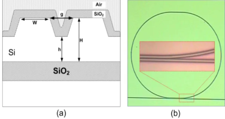
Fig. 1. (a) Cross sectional schematic view of the designed rib waveguide and the coupling region. The dimensions used in fabrication are H=1.00µm, w=1.0 µm, h=0.58µm and g=0.8µm (b) Optical micrographs of one of the fabricated resonators and its coupling region.
2. Theory and design
Detailed theoretical analysis for ring resonators can be found in many journal articles, [10]. We will, therefore, give here only some of the resultant equations. A ring resonator system is composed of a ring waveguide optically coupled to an input bus waveguide and optionally to a
second bus waveguide to drop the coupled wavelength. The optical power transmitted through the bus waveguide for single bus case is
It= | (1 −κ) 1/2 − exp(−(α T/2 + iφ)) 1− (1 −κ)1/2 exp(−(α T/2 + iφ)) |2 (1)
Here,κis the fraction of power coupled between the waveguide and the ring, so that 1−κ is the throughput portion of the power that is not coupled to the ring.αT andφ are the optical power loss and the phase accumulated per round trip in the ring, respectively and are defined asαT =αL andφ(λ) = (2π/λ0)neL for a resonator of length L, total optical loss coefficient, α, effective refractive index of ne and free space wavelength,λ0. At a particular resonance wavelength, we can get zero transmitted power at the throughput port if and only if
κ= 1 − exp(−αT) (2)
equation is satisfied. This is the so-called critical coupling condition which leads to high quality factors with the largest extinction ratios.
The design of large cross section SOI ring resonators with high Q factors starts by determin-ing the largest waveguide dimensions that satisfy sdetermin-ingle mode condition. After a preliminary estimation using effective index methods, exact dimensions of the waveguides have been de-termined after extensive numerical simulations using the three dimensional beam propagation method (BPM) feature of the BeamProp package [11]. This is followed by the estimation of the expected propagation losses which is critical in the design of SOI ring resonators with high Q factors. Measurements on straight waveguides designed and fabricated with dimensions ob-tained in the simulation step, were performed to determine the upper limit on the expected propagation losses. A cross sectional schematic view of the waveguide structure with the di-mensions used during the fabrication is illustrated in Fig. 1(a). An optical micrograph of the fabricated racetrack resonator is shown in Fig. 1(b) and the inset shows the coupling region in more detail.
In most Si rib waveguide devices, quasi single mode waveguides with large cross sections are preferred to minimize insertion losses. Design of ring resonators using SOI rib waveguides with typical widths and heights of 3µm or larger, however, leads to rings with radii larger than 10 mm due to radiation losses at smaller radii. This would lead to poor free spectral range. To obtain compact devices suitable for higher integration that have larger free spectral range, ring resonators with curvatures of submillimeter radii, are needed. Thus, smaller waveguide dimen-sions are essential for compact ring resonators. Extensive numerical calculations led to width and height of 1.00µm and slab height of 0.58µm for the final waveguide design. Recently, we have studied this structure and used it to realize a passive polarization splitter [12]. These waveguide dimensions result in a single mode pear shaped structure.
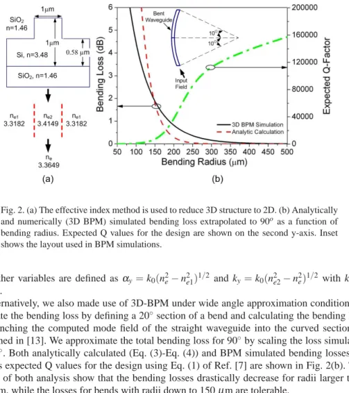
A major issue in the design of ring resonators is the estimation of bending loss. We first calculated the bending loss using a two dimensional analysis based on Marcuse’s equation for bending slab waveguides. The details of the analysis can be found in [13]. Briefly, in this approach, the 3-D waveguide structure is reduced to 2-D (See Fig. 2(a).) using the effective index method, and the resulting analysis leads to bending loss in dB’s for a given angular section∆θ(in radians) of radius R as
Lossbend= −10log(exp(−αbend∆θR)) (3) whereαbend is the optical bending loss coefficient and is given by
αbend = α2 y k30ne(1 +αyw2) ky2 (n2 e2− n2e1) exp(αyw)exp( −2α3 y 3n2 ek20 R) (4)
Fig. 2. (a) The effective index method is used to reduce 3D structure to 2D. (b) Analytically and numerically (3D BPM) simulated bending loss extrapolated to 90o as a function of bending radius. Expected Q values for the design are shown on the second y-axis. Inset shows the layout used in BPM simulations.
The other variables are defined asαy= k0(n2e− n2e1)1/2 and ky= k0(n2e2− n2e)1/2 with k0= 2π/λ0.
Alternatively, we also made use of 3D-BPM under wide angle approximation conditions to simulate the bending loss by defining a 20◦section of a bend and calculating the bending loss by launching the computed mode field of the straight waveguide into the curved section as explained in [13]. We approximate the total bending loss for 90◦by scaling the loss simulated for 20◦. Both analytically calculated (Eq. (3)-Eq. (4)) and BPM simulated bending losses, as well as expected Q values for the design using Eq. (1) of Ref. [7] are shown in Fig. 2(b). The results of both analysis show that the bending losses drastically decrease for radii larger than 300µm, while the losses for bends with radii down to 150µm are tolerable.
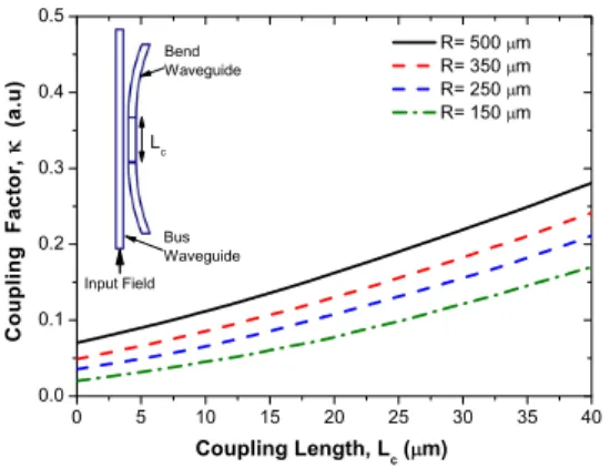
Following the determination of the range of radii that can be used in the design of ring res-onators, the coupled power factor from the bus waveguide to an adjacent waveguide bend has to be calculated. 3D BPM simulations are also employed for this purpose. A straight waveguide is placed close to a bent waveguide similar to the one used to simulate the bending losses. The optical power launched into the straight waveguide is monitored at the output of the bent waveguide (inset of Fig. 3). The minimum coupling gap is determined by the limits of opti-cal photolithography which, in our case, is 0.8µm. This value limits the gap coupling factor between the bus waveguide and the bent waveguide. To overcome this problem and increase coupling factor for critical coupling, straight waveguide sections are inserted into the bent waveguide sections in the coupling region next to the bus waveguide. This transforms our de-sign to a racetrack resonator. With a coupling gap of 0.8µm, the need for a racetrack shape becomes inevitable as the ring radii gets smaller, since coupling factor is too small for smaller radii (See Fig. 3).
Using the critical coupling condition defined in Eq. (2), and estimating the total optical loss in the resonators, one can find the necessary coupling factor. The total optical loss includes both bending and propagation losses. Bending loss is determined through BPM simulations as mentioned earlier, while the propagation loss is experimentally measured on waveguides
Fig. 3. Numerically (3D BPM) calculated coupling factors as a function of straight coupling length for different radii. Inset shows the layout used in BPM simulations
fabricated with same dimensions used for the bus waveguides of the ring resonator system. In accordance with the literature [8], we find the upper limit for propagation loss to be 5.5 dB/cm. 3. Fabrication and measurements
We fabricated the ring resonator system on Unibond SOI wafers [14], to make use of their good thickness uniformity. The top Si layer was 1µm thick with a buried oxide layer of 1µm and a handle Si layer thickness of 625µm. We started by cleaving a 15x15 mm chip from a whole wafer. After a three solvent degreasing process, a photoresist layer of about 0.75µm in thickness was spun on the top Si side of the chip. Contact photolithography was applied to transfer the patterns of resonators to the chip. The patterns were etched down by 0.42µm on the top silicon layer of the SOI chip by reactive ion etching (RIE). We used a CHF3+ O2 recipe in RIE process that results in smooth sidewalls. The RIE etch was followed by chemical cleaning of the remaining photoresist residues and deposition of about 0.9µm SiO2thick layer on the chip using plasma enhanced chemical vapor deposition, ending the device fabrication, Fig. 1(b). Finally, In order to obtain good facets, we used an aqueous KOH solution to thin the substrate down to about 150µm before cleaving the device.The final length of the chip was 7 mm.
The chip was mounted in an integrated optics measurement setup. The input optical signal was obtained from an external cavity tunable laser with a resolution of 1 pm coupled to the straight bus waveguides using a tapered and lensed fiber with a spot size of 2µm. The polar-ization of the input light was controlled by a fiber polarpolar-ization controller before being coupled to the chip. An infrared camera is used to align the fiber and the input facet. The light at the output of the bus waveguide was collected with a microscope objective and passed through a polarizer of high extinction ratio before reaching a Ge photodetector. Total insertion loss was measured to be 27 dB with unpolished facets. The transmitted optical power was obtained as a function of wavelength.
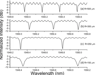
The measured TE transmission spectra of the fabricated resonators are shown in Fig. 4. for various bending radii measured at the throughput port of the ring resonator system. In addition to the sharp dips in the throughput spectrum, small amplitude oscillations due to Fabry-Perot resonances between the ends of the straight bus waveguide are clearly observed. We summarize the optical (including free spectral range (FSR), full width at half maximum (FWHM),
Q-factor and extinction ratio) as well as some physical characteristics of the fabricated resonators in Table. 1. Quality factors as high as 119000 have been observed for radii of 350 µm or larger. These Q factors are the largest reported Q values for large cross section Si rib waveguide racetrack resonators. The lower Q values for smaller radii rings are an indication of higher losses.
Fig. 4. Measured transmission spectra of the fabricated silicon-on-insulator rib waveguide racetrack resonators for radii of 500, 350, 250 and 150µm for the same span of wave-lengths.
Table 1. Summary of characteristics of fabricated and measured resonators
Radius (µm) Lc(µm) FSR (pm) FWHM (pm) Q-Factor Extinction Ratio (dB)
500 2 205 13 119000 7.8
350 32 290 13 119000 10.4
250 26 490 17 91000 12.2
150 38 630 35 44000 10.8
4. Conclusion
In summary, we have presented design, fabrication and optical characterization of high-Q SOI ring resonators with single mode large cross section waveguides. Using standard optical pho-tolithography technology, the quality factor, Q values reported in this work are the highest Q values achieved in the SOI platform, excluding submicron Si wire resonators. The experimental Q values for smaller radii are larger than expected, indicating lower losses than assumed in the design. It is clear that we do not achieve perfect critical coupling which would results in lower than maximum Q-factor [7], while low coupling factor results in low extinction ratio. Our re-sults show that we reach a good compromise between good extinction ratios and high quality factors.
Acknowledgments