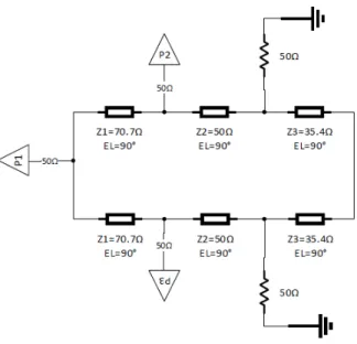
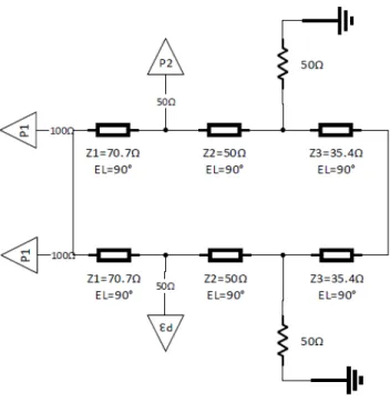
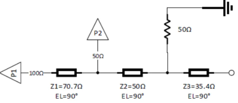
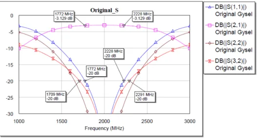
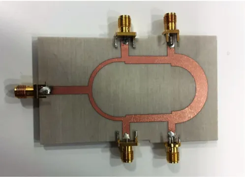
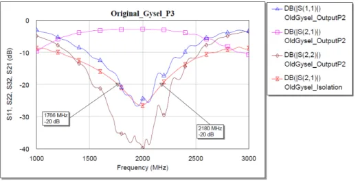
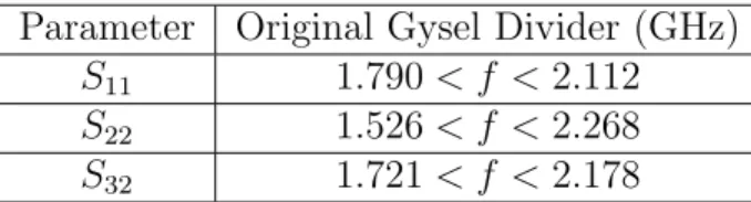
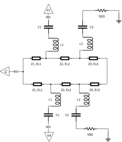
A modified wideband Gysel power divider structure
Tam metin
Şekil
Benzer Belgeler
Azadirachtin uygulanan gruplarda kontrol gruplarına göre gözlemlenen bu artmaların istatistiksel olarak da önemli olduğu analizlerle belirlendi ve deney
We demonstrate red-shifting absorption edge, due to quantum confined Stark effect, in nonpolar InGaN/GaN quantum structures in response to increased electric field, while we show
PAU İlahiyat Fakültesi Dergisi (Pauifd) Güz 2018, Cilt: 5, Sayı: 10, s: 305-329 Belirtildiği gibi İbn Sînâ dış ve iç idrak güçlerinin verileriyle dış dünya ile beraber
Sonra, 22 sayısı çift olduğu için 2’ye bölüyoruz, 11 sayısına gönderiyoruz.. Buradan tek- rar 3x11+1=34 sayısına, oradan 17’ye, 17’den 52’ye ve böyle- ce
Efekta General English B1-1, B1-2, B1-3 düzey ders kitaplarında okuma ve yazılı anlatım etkinliklerine ayrılan etkinlik ve alıştırma sayısının dinleme,
Fotoğraf 3: Üç Ayak Gücü Düzeneği Fotoğraf 4: Demir Çubuk, Kolan Dokuma Tezgâhı Kaynak: (Fotoğraf 3) Yüceer Arslan, 2014:127, (Fotoğraf 4) Serpil Erdeliğ Demirbaş,
1) Bir sayının 27 eksiği 37 ediyor. Bu sayı kaçtır? 8) Emin , 48 ve 44 sayılarını kullanarak çıkarma işlemi yaptı. 28 fındığı tabaktan alırska tabakta kaç
The maximum average result of 30 classification steps with 30 randomly selected test samples is observed with 12 neurons in the hidden layer for 7 hours sleep recording as 87.5%.
