LOW DIMENSIONAL STRUCTURES FOR
OPTICAL AND ELECTRICAL
APPLICATIONS
a thesis
submitted to the department of physics
and the institute of engineering and science
of bilkent university
in partial fulfillment of the requirements
for the degree of
master of science
By
˙Imran Ak¸ca
I certify that I have read this thesis and that in my opinion it is fully adequate, in scope and in quality, as a thesis for the degree of Master of Science.
Prof. Dr. Atilla Aydınlı(Advisor)
I certify that I have read this thesis and that in my opinion it is fully adequate, in scope and in quality, as a thesis for the degree of Master of Science.
Prof. Dr. S¸efik S¨uzer
I certify that I have read this thesis and that in my opinion it is fully adequate, in scope and in quality, as a thesis for the degree of Master of Science.
Assist. Prof. Dr. Ceyhun Bulutay
Approved for the Institute of Engineering and Science:
Prof. Dr. Mehmet B. Baray Director of the Institute
ABSTRACT
LOW DIMENSIONAL STRUCTURES FOR OPTICAL
AND ELECTRICAL APPLICATIONS
˙Imran Ak¸ca M.S. in Physics
Supervisor: Prof. Dr. Atilla Aydınlı July, 2008
Low dimensional structures such as quantum dots have been particularly attrac-tive because of their fundamental physical properties and their potential appli-cations in various devices in integrated optics and microelectronics. This thesis presents optical and electrical applications of low dimensional structures. For this purpose we have studied silicon and germanium nanocrystals for flash memory applications and InAs quantum dots for optical modulators.
As a quantum dot, nanocrystals can be used as storage media for carriers in flash memories. Performance of a nanocrystal memory device can be expressed in terms of write/erase speed, carrier retention time and cycling durability. Charge and discharge dynamics of PECVD grown nanocrystals were studied. Electron and hole charge and discharge currents were observed to differ significantly and strongly depend on annealing conditions chosen for the formation of nanocrystals. Our experimental results revealed that, discharge currents were dominated by the interface layer acting as a quantum well for holes and route for direct tunneling for electrons.
On the other hand, possibility of obtaining quantum dots with enhanced electro-optic and/or electro-absorption coefficients makes them attractive for use in light modulation. Therefore, waveguides of multilayer InAs quantum dots were studied. Electro-optic measurements were conducted at 1.5 µm and clear Fabry-Perot resonances were obtained. The voltage dependent Fabry-Perot mea-surements revealed that 6 V was sufficient for full on/off modulation. Electro-absorption measurements were conducted at both 1.3 and 1.5 µm. Since the structure lases at 1285 nm, high absorption values at 1309 nm were obtained. The absorption spectrum of the samples was also studied under applied elec-tric field. Absorption spectra of all samples shift to lower photon energies with
iv
increasing electric field.
Keywords: Silicon nanocrystals, Germanium nanocrystals, nonvolatile memories,
quantum dots, electro-optic modulation, electro-absorption modulation, optical waveguides.
¨
OZET
D ¨
US¸ ¨
UK BOYUTLU YAPILARIN ELEKT˙IR˙IK VE
OPT˙IK UYGULAMALARI
˙Imran Ak¸ca
Fizik B¨ol¨um¨u, Y¨uksek Lisans Tez Y¨oneticisi: Prof. Dr. Atilla Aydınlı
Temmuz, 2008
Kuvantum nokta gibi d¨u¸s¨uk boyutlu yapılar, sahip oldukları fiziksel ¨ozellikleri, optik ve mikro-elektronikteki geni¸s uygulama alanları ile olduk¸ca ilgi ¸cekmektedir. Bu tezde d¨u¸s¨uk boyutlu yapıların optik ve elektrikteki uygulamalarindan bahsedilmektedir. Bu ama¸cla silikon ve germanyum nanokristal i¸ceren kalıcı hafızalara ve InAs kuvantum nokta i¸ceren optik kipleyicilere y¨onelik ¸calı¸smalar yapılmı¸stır.
Aslında birer kuvantum nokta olan nanokristaller y¨uk depolayabildikleri i¸cin kalıcı hafıza olarak da kullanılabilmeleri olasıdır. Nanokristal belleklerin per-formansı yazma/silme hızı, y¨uk tutma s¨uresı ve devir s¨uresi ile belirlenmekte-dir. PECVD metodu ile ¨uretilen nanokristalerin ¸sarj ve de¸sarj ¨ozellikleri ince-lenmi¸stir. Elektron ve de¸siklerin ¸sarj, de¸sarj akımlarının pi¸sirme sıcaklıklarına ba˘glı olarak birbirinden farklılık g¨osterdi˘gi g¨ozlemlenmi¸stir. Deney sonu¸clarına g¨ore, de¸siklerin de¸sarj akımının kuvantum kuyusu gibi davranan ara y¨uz tabakası tarafından, elektronların de¸sarj akımının ise direk t¨unelleme tarafından sa˘glandı˘gı g¨ozlemlenmi¸stir.
Di˘ger taraftan, kuvantum noktaların y¨uksek elektro-optik ve elektro-so˘gurma katsayılarına sahip olma olasılıkları, bu malzemeleri ı¸sı˘gın mod¨ulasyonu a¸cısından olduk¸ca ¨onemli kılmaktadır. Bu ama¸cla, InAs kuvantum noktalar i¸ceren dalga kılavuzu yapıları uzerinde calı¸sılmı¸stır. Elektro-optik ¨ol¸c¨umleri 1.5 µm dalga boyunda ger¸cekle¸stirilmi¸s ve Fabry-Perot rezonansları elde edilmi¸stir. Fabry-Perot ¨ol¸c¨umlerinin sonu¸clarına g¨ore, 6 V i¸cin ı¸sık tamamen a¸cılıp ka-patılabilmektedir. Elektro-so˘gurma ¨ol¸c¨umleri 1.3 ve 1.5 µm dalga boylarında ger¸cekle¸stirilmi¸stir. Kullanılan yapılar ger¸cekte lazer olarak tasarlanmı¸s ve 1285 nm’de ı¸sıyan yapılar oldukları i¸cin en y¨uksek so˘gurma de˘gerleri 1309 nm’de
vi
elde edilmi¸stir. So˘gurma e˘grileri uygulanan gerilim altında incelenmi¸s ve artan gerilimle beraber so˘gurma e˘grilerinin d¨us¨uk foton enerjilerine do˘gru kaydıkları g¨ozlemlenmi¸stir.
Anahtar s¨ozc¨ukler : Silikon nanokristal, Germanyum nanokristal, kalıcı hafıza,
kuvantum nokta, elektro-optik mod¨ulasyon, elektro-so˘gurma mod¨ulasyon, optik dalga kılavuzları .
Acknowledgement
First and foremost, I would like to thank my research advisor, Professor Atilla Aydınlı. I knew Professor Aydınlı since I was a first year senior student. He offered me an excellent opportunity, when I asked about working in his laboratory during the summer. I have been happily working for Professor Aydınlı ever since. I admire his personality and broad knowledge very much. He helped me generously and gave me tremendous support over the years. I have benefited a lot from his continuous encouragement and invaluable advice. I am also very impressed by his enthusiasm for the scientific pursuit. I feel very fortunate for the opportunity to have him as my research advisor.
I am very thankful to Assistant Professor Aykutlu Dana. I learned a lot from him in both experimental and theoretical analysis of the nanocrystal nonvolatile memories. He has been supportive of my work and I also enjoyed taking his excellent courses.
I am indebted to the former members of the Integrated Optics Group, Feridun Ay, ˙Isa Kiyat, and Selcen Aytekin for helping me get through the initial learning stage as a new integrated optics group student.
I am also thankful to the current members of the Integrated Optics Group, A¸skın Kocaba¸s, Ay¸se Erbil, Se¸ckin S¸enlik, and Samet Yumruk¸cu for their friend-ship and support.
I am also particularly grateful to Selim Ol¸cum for his friendship and numerous technical discussions.
I would like to thank Professor Ra¸sit Turan at Middle East Technical Uni-versity, Turkey, Professor Nadir Da˘glı at University of California, Santa Barbara, USA for the discussions and collaboration. I am also grateful to Professor An-drea Fiore at Ecole Polytechnique Federale de Lausanne (EPFL), Switzerland for InAs quantum dot samples, and Assistant Professor Aykutlu Dana for germanium nanocrystal samples.
viii
I would also like to thank our laboratory physicist, Murat G¨ure and technician Erg¨un Karaman for their technical support during my research.
I would like to acknowledge Umut Bostancı, for collaborations on silicon nanocrystal optical waveguide project. I am very grateful to him for his sup-port in clean room processes.
I am also grateful to the numerous help from other clean room folks. Among them were M¨unir Dede, Rohat Melik, and Tuncay ¨Ozel.
I am also appreciative of the financial support I received through a fellowship from T ¨UB˙ITAK.
I would like to thank to all staff of the Institute of Materials Science and Nanotechnology for their invaluable support during my research.
I am also thankful to the directors of the UNAM, Professor Salim C¸ ıracı and Assistant Professor Mehmet Bayındır for providing excellent facilities in UNAM. I would like to thank my family and Akın Avcı for their love, support and encouragement.
Finally, I want to thank and acknowledge my thesis examination committee: Professors Atilla Aydınlı, Ceyhun Bulutay, and S¸efik S¨uzer.
Contents
1 Introduction 1
1.1 Fundamentals of Nanoparticles . . . 1
1.1.1 Silicon and Germanium Nanocrystals . . . 2
1.1.2 Quantum Dots . . . 5
1.2 Thesis Outline . . . 7
2 Silicon and Germanium Nanocrystal MOS Capacitors for Mem-ory Applications 9 2.1 Introduction . . . 9
2.2 Experimental . . . 12
2.2.1 Preparation of Germanium Nanocrystals . . . 12
2.2.2 Preparation of Silicon Nanocrystals . . . 13
2.2.3 Fabrication of Nanocrystal MOS Capacitors . . . 21
3 Modelling of Nanocrystal MOS Capacitors 24 3.1 Fundametals of MOS Capacitors . . . 24
CONTENTS x
3.2 Basic Conduction Mechanisms for MOS Capacitors . . . 27
3.3 Fundamentals of Nanocrystal MOS capacitor . . . 29
3.3.1 Charging of Nanocrystal MOS capacitors . . . 29
3.3.2 Discharging of Nanocrystal MOS Capacitors . . . 30
4 Electrical Characterization of Nanocrystal MOS Capacitors 34 4.1 Germanium Nanocrystal MOS Capacitors . . . 34
4.1.1 High Frequency Capacitance-Voltage Measurements . . . . 34
4.1.2 Flat-band Voltage Measurements . . . 35
4.1.3 Charging of Nanocrystals . . . 36
4.1.4 Discharging of Nanocrystals . . . 37
4.2 Silicon Nanocrystal MOS Capacitors . . . 39
4.2.1 Flat-Band Measurements . . . 39
4.2.2 Charging of Nanocrystals . . . 42
4.2.3 Discharging of Nanocrystals . . . 42
4.3 Conclusions . . . 43
5 Electro-optic and Electro-absorption Properties of InAs Quan-tum Dot Waveguides 45 5.1 Introduction . . . 45
5.2 InAs Quantum Dot Waveguides Under Applied Field . . . 50
CONTENTS xi
5.2.2 Measurement Set-up . . . 51
5.3 Simulations of InAs Quantum Dot Waveguides . . . 52
5.4 Measurements and Results . . . 55
5.4.1 Electro-optical Measurements . . . 55
5.4.2 Electro-absorption Measurements . . . 58
5.5 Conclusions . . . 60
List of Figures
2.1 Plama enhanced chemical vapor deposition mechanism. . . 12 2.2 Formation of Ge NCs as a function of anneal temperature and
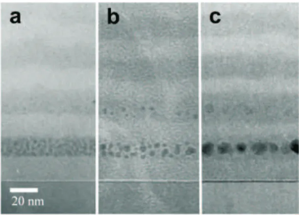
GeH4 flow rate as observed by TEM. Multi-layer structures of
germanosilicate with flow rates of 120, 110, 100 and 90 sccm are seen away from the substrate (bottom to top) after annealing at a) 650oC, b) 770 oC, and c) 850 oC for 5 minutes. . . . 14
2.3 Experimental set-up of the photoluminescence . . . 15 2.4 Effect of Si concentration on the photoluminescence. Si rich
sili-con nitride films with varying NH3 flow rates were investigated.
Note that the redshift in photoluminesce curve with increasing Si concentration. . . 16 2.5 Effect of annealing temperature and time on the
photolumines-cence. Annealed and unannealed Si rich silicon dioxide films were used for this experiment. The PL curve is maximum for 1200 oC
and 1 hour annealing conditions. . . 18 2.6 Set-up for ellipsometry measurements. . . 19 2.7 Ellipsometric study of Si-rich SiO2 films with varying annealing
temperatures and times. . . 20
LIST OF FIGURES xiii
2.8 Refractive index values of Si-rich silicon nitride film between 500 and 1000 nm. . . 21 2.9 Nanocrystal MOS fabrication fabrication steps. . . 22 2.10 (a) A glass barrier is placed over a part of the silicon substrate
for shielding the plasma. Under this barrier no material growth is observed. (b) This figure illustrates the structure of the sample after PECVD gradient growth method. . . 23
3.1 A MOS capacitor structure with Si-ncs are used as floating gate. . 25 3.2 a)During accumulation, electrons detrapped from nanocrystals
with the applied positive gate voltage.b) . . . 26 3.3 During inversion electrons trapped inside the nanocrystals by
ap-plying negative positive voltage to the gate electrode. . . 27 3.4 Schematic representation of the Fowler Nordheim tunneling under
high voltage. In here ΦB barrier height, EF M metal Fermi level,
EF Ssemiconductor Fermi level, doxoxide thickness, dF N tunneling
distance, and Vgate gate voltage . . . 28
4.1 Experimental data of charging of n (right) and p (left) type ca-pacitors. Charging currents as a function of charge voltage are measured for samples annealed at 700-800oC. . . . 36
4.2 Discharge current densities as a function of time for n and p type devices (in terms of substrate types). The holes decay faster than the electrons for samples annealed at low temperatures whereas they decay much slower for samples annealed at higher temperatures. 37
LIST OF FIGURES xiv
4.3 Band structure of Ge nanocrystal MOS capacitor, a) annealed at low temperatures, b) annealed at high temperatures. Note the ef-fect of quantum well at the interface and the increased nanocrystal size. . . 39 4.4 Cumulative flat-band voltage shift as a function of pulse voltage.
Tunnel oxide layer was grown by gradient growth method. The dip beyond 15 V indicates the in-layer charge motion. . . 40 4.5 For this sample gradient growth method was applied to the
nanocrystal formation layer. At 15 V of pulse voltage in-layer charge motion is seen which corresponds to a negative hysteresis. . 41 4.6 Cumulative flat-band voltage shift of the sample which was not
grown by gradient growth method. Charge motion is observed inside the nanocrytstal layer and at the oxide-nitride interface at specific voltages. . . 41 4.7 Cumulative flat-band voltage shift of the stoichiometric sample as
a function of the pulse voltage. Note that there is no in-layer charge motion for this sample. . . 42 4.8 Decay of the stored charges of the Si-nc MOS capacitors which has
a gradually increasing layers. With increasing thickness decay rate of the charges decreases. . . 43
5.1 EL data and detailed structure of the InAs quantum dot waveguides. 51 5.2 Measurement set-up for electrical and optical measurements. . . . 52 5.3 Fundamental mode profile of the InAs quantum dot waveguides for
TE polarization. The effective index of the structure is obtained as 3.27 from simulation. . . 54
LIST OF FIGURES xv
5.4 Fundamental mode profile of the InAs quantum dot waveguides for TM polarization. The effective index of the structure is obtained as 3.248 from simulation . . . 54 5.5 Fabry-Perot resonances at 1515 nm for 6 Volt reverse bias. The
dots show the experimental data and the line indicates the opti-mum curve fit. . . 56 5.6 Voltage dependent shift of Fabry-Perot resonances. Significant
tuning is observed with relatively low voltages. . . 56 5.7 Variation in refractive index as a function of applied voltage at 1515
nm. The dots show the experimental data and the line indicates the linear fit. . . 57 5.8 The graphical representation of the calculation of overlap factor.
The confinement factor is calculated from this overlap region by simply integrating the shaded area. . . 59 5.9 Change in absorption due to applied reverse bias for 1 mm long
sample. Red shift of the spectra should be noted with increasing applied voltage. . . 60 5.10 Change in absorption due to applied reverse bias for 1.6 mm long
Chapter 1
Introduction
1.1
Fundamentals of Nanoparticles
Nanoparticles are zero-dimensional structures with a diameter varying between one to few hundreds of nanometers. When the dimensions of the material are scaled down to nanometer range, the atomic and electronic structures may gain some unique features which make the material favorable for many applications. The properties of the nanoparticles are mostly size dependent. For small nanopar-ticles, the properties vary and they are specific to each size. At large sizes, nanoparticles would have the properties similar to bulk.
The main mechanism that triggers the unusual behavior of the nanoparticles is quantum confinement. Quantum confinement model is based on the effective-mass approximation theory. It is an inherent concept for all the low-dimensional structures, such as quantum wells, quantum wires, and quantum dots, which display confinement in 1, 2 and 3 dimensions, respectively.
Quantum confinement becomes effective when the particles dimensions are comparable to exciton Bohr radius. According to the quantum confinement the-ory, electrons in the conduction band and holes in the valence band are confined spatially by the potential barrier. Bound states are formed in the quantum wells
CHAPTER 1. INTRODUCTION 2
energies of which are determined by the potential of the barrier and the well width as well as other material parameters. The case of the quantum dots represent the ultimate confinement configuration with discrete energy states due to confinement in all directions. The density of states also changes dramatically from the bulk case, reducing along the direction of confinement and ultimately reaching atom like discrete states. It is well known from basic quantum mechanics that as the width of the spatial confinement decreases energy separation between the bound states increases. Therefore, the energy that is required for the optical transition from valence band to conduction band increases and as a result, effective band gap increases relative to the bulk value [31].
Thus, quantum confinement model can also explain the blue shift of the lumi-nescence spectrum with decreasing of the particle size. According to the model, the emission wavelength and intensity depend on the nanoparticle diameter, size distribution, and concentration.
Nanoparticles can be amorphous or crystalline and when they are crystalline they are called as nanocrystals. In this thesis, we will mainly concentrate on silicon nanocrystals (Si-nc) and germanium nanocrystals (Ge-nc).
1.1.1
Silicon and Germanium Nanocrystals
Silicon is the material of choice in the microelectronic industry. This remarkable success is due to various factors such as the wide availability of silicon and its good thermal and mechanical properties that make it easy to manufacture silicon based devices. On the other hand, silicon has an indirect band-gap structure that limits the optical emission and hence modulation.
Porous silicon was the first material that has been reported to display an intense photoluminescence [8]. After that, Si-ncs have become popular for their relatively high quality of luminescence efficiency properties. The luminescence of Si nanocrystals has been studied in single layer and multi layer structures and relatively high efficient electroluminescence (EL) values were obtained [9].
CHAPTER 1. INTRODUCTION 3
Si-ncs and Ge-ncs may have a radii close to or smaller than the exciton Bohr radius. Once the diameter becomes smaller than the exciton radius, the energy levels in the particle become quantized and the transitions are locked into specific energy states. The term silicon nanocrystal refers to a range of materials around the transition region from amorphous to microcrystalline phase in the silicon thin film. It is similar to amorphous silicon (a-Si) but it has many useful advantages over the a-Si in the extreme limit of small size. First, if grown properly it can have a higher electron mobility. Second, it shows increased absorption in the red and infrared wavelengths, which makes it an important material for use in solar cells. Third, it has lower hydrogen concentration.
Ge-ncs have smaller band gap compared to silicon. Therefore, Ge-ncs are thought to be better suited for data retention operations than Si-ncs in non volatile memory applications.
There is a impressive number of papers in the literature reporting that pho-tonic excitation of Si-ncs and Ge-ncs induces a strong luminescence [15, 38]. Typ-ically, the luminescence spectrum covers the visible and the near-infra red regions, from 600 nm to 1000 nm. The physical mechanisms associated with luminescence is still controversial. Different models have been proposed to explain both the intense luminescence and the higher photon energy. The quantum confinement model is widely used to explain experimental results. Due to the quantum con-finement effect, the luminescence spectrum of the nanocrystals shifts to lower photon energies (blue shift) with decrease of the nanocrystal size, and enhanced emission is observed.
According to quantum confinement model, the energy that is required for the emission of a photon, depends on the nanocrystal size. Brus et.al proposed an analytical model to relate the quantum confinement effect and confinement radius in nanocrystals. When the higher order terms are neglected, the relationship between the energy and size is given as [5]:
Eg,N C = Eg,bulk− 1.8q2 e ²R + ¯h2π2 2µR2 + O µ 1 R3 ¶ (1.1)
CHAPTER 1. INTRODUCTION 4
where Eg,N C is the lowest eigenvalue for the confined exciton, Eg,bulk is the
bulk material bandgap, µ is the reduced mass of the electron-hole pair, and R is the radius of the nanocrystal . The factor 1.8 that appears in Coulomb attraction term accounts for the overlap of electron and hole wave functions.
Several different techniques have been used to produce Si-nc and Ge-ncs such as: plasma enhanced chemical vapour deposition (PECVD) [20], sputtering depo-sition [47], pulsed laser depodepo-sition (PLD) [48], physical vapour depodepo-sition (PVD) [52], ion implantation [13], all followed by thermal annealing. Extensive studies have been carried out to better understand the basic mechanisms of nanocrystal production and growth. Experimental PL and EL emission from these nanocrys-tals typically depend on both the nanocrystal size as well as the size distribution of these nanocrystals.
Si and Ge nanocrystal based devices become popular after the realization of unique properties of the nanocrystals. Si-nc and Ge-nc based photoluminescent displays, light emitting diodes (LED), optical waveguides and non-volatile mem-ories have been extensively studied.
Meldrum et al. have been active in the area of Si-nc array photoluminescent displays. They have fabricated Fabry-Perot microcavity resonators by growing a silicon rich oxide (SRO) layer between two silver films of 200 nm and 20 nm, followed by annealing at 500 oC. A HeCd laser emitting at 325 nm was used
for the PL excitation. By varying the SRO layer thickness, they tuned the light emission in the range from 475 nm to 875 nm, covering most of the visible region. The emitted light was bright enough to be recordable by means of a digital camera [32].
Enhanced light emission of the Si-ncs triggered the research on Si-nc based light emitting diodes and a huge number of article has been published on this topic [14, 21]. The first reported result on the fabrication of Si-nc based LEDs was obtained with porous n-doped silicon. A thin (12 nm) gold layer was used for the contact. In 1996, Hirschman et al. published possibly the first attempt to integrate a Si-nc (PS) LED with microelectronic circuit [14]. In their work, they used a bipolar transistor to modulate light emission in controlling the current
CHAPTER 1. INTRODUCTION 5
flow through the LED. The most efficient Si-nc based LED has been obtained by Cho and co-workers who reported an external quantum efficiency of 1.6% [21]. The Si-nc were produced in a silicon nitride layer by PECVD and was sandwiched between n-type SiC and p-type Si.
In an effort to further improve the current status of the flash memories many approaches are under study including the use of nanocrystals. Nanocrystal based non volatile memories is therefore a popular topic among the others. The charge, discharge and retention dynamics of the Si-ncs memories are being studied and the obtained results are promising. In the first part of this thesis, we study the electrical properties of semiconducting nanocrystal based MOS capacitors in order to understand their charge and dischage characteristics. This work is a good example of an electrical application of low dimensional structures in the form of nanocrystals.
1.1.2
Quantum Dots
One of the major problems involved in nanocrystal research is the inhomogeneity of the particles which causes inhomogeneous broadening effects in the PL and EL spectrum. This problem can be minimized by preparing uniform nanoparticles in the form of quantum wells, wires, or dots.
Quantum dot is a zero dimensional structure which is spatially confined in three dimensions and is characterized by a completely discrete energy spectrum. Such structures can be produced by modern epitaxial growth techniques. The epitaxial growth techniques have a very slow growth rate, which allow one to control very accurately the dimension in the growth directions. The well known epitaxial growth techniques of molecular beam epitaxy (MBE) and metal organic chemical vapor deposition (MOCVD) achieve monolayer control in the growth direction.
The Stranski-Krastanov growth mechanism is used to explain formation of self-assembled quantum dots in MBE and MOCVD systems. In this method,
CHAPTER 1. INTRODUCTION 6
the lattice mismatch between substrate and the deposited material results in strain in the crystal lattice. As more material is deposited, it eventually be-comes energetically more favorable for the material to form islands. As a result, three-dimensional islands are formed rather than a uniform film. Density and size of these quantum dots can be controlled using computer controlled growth conditions.
This thesis is concerned specifically with the InAs/InGaAs combination. The lattice constant of InAs is approximately 7% greater than the lattice constant of InGaAs. When InAs is deposited on InGaAs layer, significant strain develops at the interface. Beyond a critical thickness of InAs, the growth mode changes from layer-by-layer growth to the formation of three-dimensional islands. When the InAs islands are capped with a second layer of InGaAs, the islands form three dimensional potential wells, known as self assembled quantum dots. These quantum dots typically have base sizes of 10 nm, but much less is known about their physical size, shape and composition.
Quantum dots are particularly significant for optical applications due to their theoretically high quantum yield. They are specifically intented for use in tum computing, laser, light emitting diodes, and photovoltaic devices. The quan-tum dot lasers will be discussed in this section.
Semiconductor lasers are key components in optical communications. The basis of laser operation depends on the creation of nonequilibrium populations of electrons and holes. In 1970, C. Henry proposed that, using quantum wells as the active layers in a laser would result in more efficient devices operating at lower threshold currents than lasers with bulk active layers. In addition, the use of a quantum well, provides the tuning capability of the wavelength. In 1975, the first quantum well laser was demonstrated, but it was many times less efficient than a conventional laser. After the realization of new materials growth capabilities (MBE), more efficient structures have been fabricated.
Quantum dots were the promising materials for lasers. Arakawa and Sakaki predicted that quantum dot lasers should exhibit less temperature dependent performance than existing semiconductor lasers [4]. Other benefits of quantum
CHAPTER 1. INTRODUCTION 7
dot active layers include further reduction in threshold currents and an increase in differential gain. Thus, quantum dot lasers with high quality, uniform quantum dots in the active layer have become popular.
Fiore et al. have worked on InAs/GaAs quantum dot lasers and obtained high gain values for these structures [16]. They built InAs quantum dot based quantum dot laser lasing at 1280 nm using a ridge waveguide structure. The quantum dots were sandwiched between a p-type and an n-type layer to form a p-n junction. Quantum dot lasers were studied under forward bias. However, little is known on the reverse biased characteristics of these structures. In the second part of this thesis, we report the electro-optical properties of these InAs quantum dots for possible use in optical modulators.
1.2
Thesis Outline
This thesis presents optical and electrical applications of low dimensional struc-tures. The chapters are organized as follows:
In Chapter 2, we discuss the design, fabrication, and characterization of silicon and germanium nanocrystal layers made by plasma enhanced chemi-cal vapor deposition. Photoluminescence, raman scattering, transmission elec-tron microscopy, and ellipsometry measurements are used for characterization of nanocrystals. Moreover, the effects of the nanocrystal size, density and anneal-ing temperature and time on the photoluminescence are studied. Finally, the fabrication of Si-nc and Ge-nc MOS capacitors are presented.
In Chapter 3, the modelling of the charging and discharging mechanism of silicon and germanium nanocrystal MOS capacitors are studied. These devices are silicon and germanium nanocrystal floating gate MOS capacitors designed to correlate the optical properties of silicon and germanium nanocrystals to the charging and discharging mechanisms. We use the model that we proposed earlier, which assumes charge storage in quantized energy levels of nanocrystal instead of deep traps.
CHAPTER 1. INTRODUCTION 8
In Chapter 4, charge and discharge measurements of nanocrystal MOS capac-itors are explained and results are given. Electron and hole charge and discharge dynamics are studied. Electron and hole charge and discharge currents are ob-served to differ significantly and depend strongly on annealing conditions chosen for the formation of nanocrystals. At low annealing temperatures, holes are seen to charge slower but to escape faster than electrons. They discharge slower than electrons when annealing temperatures are raised. We demonstrate that discharge currents are dominated by the interface layer acting as a quantum well for holes and by direct tunneling for electrons.
Chapter 5 describes the electro-absorption and electro-optical properties of InAs quantum dot waveguide structures under an applied electric field. After giving the definition of electro-optic and electro-absorption effects, the test de-vices are described in detail. The electrical and optical characterization of the structures are explained and the measurement set-up is given. For electro-optic measurements, the Fabry-Perot Interferometer method is used and the voltage dependent Fabry-Perot resonances are obtained. The experimental results are fit-ted to well known Fabry-Perot transmission formula and electro-optic coefficient for InAs quantum dots is obtained. The results reveal that enhanced electro-optic coefficient is obtained for InAs quantum dot based ridge electro-optical waveguides compared to bulk GaAs. For electro-absorption measurements, optical transmis-sion experiments are conducted under varying voltages. The results indicate that with increasing voltage change in absorption increases and absorption edge shifts to lower photon energies. The electro-optical and the electro-absorption demon-strates that InAs quantum dots are good candidates for modulator applications. In Chapter 6, a brief summary of the performed studies and the conclusions reached are given and future directions for research in these topics are suggested.
Chapter 2
Silicon and Germanium
Nanocrystal MOS Capacitors for
Memory Applications
2.1
Introduction
Recently, nonvolatile memory devices utilizing nanocrystals in floating gate de-vices have received considerable attention due to their promising memory perfor-mance and high scalability. In nanocrystal memory devices, nanocrystals such as semiconductors [39], metals [23], and compound semiconductors [51] are sand-wiched between the control oxide and the tunneling oxide layers as charge storage nodes to replace the continuous floating gate layer which are used in conventional memories.
The nonvolatile Si-nc and Ge-nc memories have been extensively studied. A complete review of the literature exceeds the scope of this thesis, so we will briefly review some general features reported in the literature focusing especially on charge and discharge dynamics of carriers in nanocrystal memories.
CHAPTER 2. NANOCRYSTAL MOS CAPACITORS 10
Busseret et al. have studied nonvolatile memory devices, which were basi-cally MOS capacitors. The polysilicon floating gate was replaced by LPCVD grown Si-ncs where nanocrystals acts as storage node. They showed that the ap-proach of De Salvo on charge and discharge dynamics of the nanocrystals is not completely appropriate for experimental observations. They proposed a so-called granular model in which electrons interact with the nanocrystals one by one. The experimental results indicated that charge dynamics of Si-ncs were related to the number of Si-ncs occupied by one charge and not to the average number of charges per Si-nc [6].
Campera and Iannaccone have studied the charging and discharging processes in Si-nc flash memories during write/erase operations. As a result of the exper-imental studies and numerical simulations, they have shown that electrons are stored in quantum confined states in the nanocrystal conduction band. They have also focused on the effect of hydrogen annealing on the role of traps in the nanocrystals during charging and discharging mechanisms [7].
Yang et al. have observed the charge trapping and retention in Ge-ncs. For this purpose, a MOS structure with Ge-ncs distributed in the gate oxide was fabricated. Ge-ncs were synthesized using the low-energy Ge ion implantation which was followed by a thermal annealing at 800 oC. They have observed that,
electron trapping had occurred at both negative and positive charging voltages, on the other hand holes were trapped at only positive charging voltages. The retention time of the electrons are long in the case of positive charging [29].
She et al. have studied the write/erase speed of Ge-nc memory devices. By using single-charge tunneling theory, they have proposed a model to describe the retention. The effects of nanocrystal size, tunnel-oxide thickness, and high-k tunnel material on the device performance were studied. They have shown that Ge-nc memory devices could provide at least 106 times larger retention-time to
write-time ratio than conventional floating-gate devices. They have proposed that the device performance could be enhanced using high-k, and low barrier tunel materials [44].
CHAPTER 2. NANOCRYSTAL MOS CAPACITORS 11
Koh et al. have worked on effects of traps on charge and discharge mecha-nisms of Ge-nc memories. Transistor and capacitor structures with Ge-ncs were fabricated to study the trap energy levels. Temperature dependent measurements were conducted to observe the effect of the traps on Ge-nc charging dynamics. Nanocrystal size and the trap energy-level relationship for a long-term charge retention performance was extracted from simulation results [22].
Sousa et al. have presented electron- and hole-based data storage operations in Si1−x-Gex nanocrystal nonvolatile memories. Due to the lower confinement
barrier, electrons are removed much faster than holes which makes holes more appropriate for long charge retention operations. The only disadvantage of the hole-based operation was slower data programming in comparison to electrons. Additionally, they have observed that that the increase of Ge composition reduces the electron retention time [12].
Kanoun et al. have investigated the charging effects in Ge-ncs embedded in SiO2 matrix fabricated by LPCVD technique. They have used
capacitance-voltage (CV) and currentcapacitance-voltage (IV) analysis. In C-V measurements, a hysteresis was observed which indicates that holes are charging in the Ge islands. Different ramp times were used in C-V measurements to demonstrate the hole charging is the origin of the transient current. I-V measurements have demonstrated the charging effects and hysteresis was observed only at low temperatures [28].
Despite all of the above, charge and discharge characteristics of nanocrystal and where the charges are stored are not well known. We, therefore, in this thesis study the charge and discharge characteristics of nanocrystals and explore the possibility of charge storage in the quantized levels of the nanocrystals. Effects of high temperature annealing on the performance of the nanocrystal based MOS capacitors are also presented.
CHAPTER 2. NANOCRYSTAL MOS CAPACITORS 12
2.2
Experimental
2.2.1
Preparation of Germanium Nanocrystals
PECVD Deposition
Plasma-enhanced chemical vapor deposition (PECVD) is a technique com-monly used in micro-fabrication to deposit layers of insulating materials and amorphous or polycrystalline silicon. The plasma is used to help stimulate a reaction on the substrate surface of two or more spices from the gas phase. The major advantage of PECVD is, its lower temperature capability with respect to other systems, such as conventional CVD. For example, for silicon deposition in a CVD system , the required temperature is 700-900 oC, on the other hand, this
value decreases to 250-350oC in a PECVD system. The schematic representation
of a PECVD system is given in Figure 2.1.
Chamber RF Temperature Roughing Pump Clean NH3 N2 N O2 NO2 SiH4 sample Vent Line APC
Figure 2.1: Plama enhanced chemical vapor deposition mechanism.
The germanosilicate films were grown using a parallel-plate type PECVD reactor (Plasmalab 8510C). 180 sccm SiH4(2% in N2), 225 sccm NO2 and varying
flow rates of GeH4 (2% in He) were used. The sample temperature and process
pressure were 350 oC, 1000 mTorr, respectively. 10 W of RF power was applied
during the deposition. After deposition, germaniumsilicate films were annealed at high temperature in order to provide phase seperation between oxide and
CHAPTER 2. NANOCRYSTAL MOS CAPACITORS 13
germanium. Annealing
In Ge-nc formation processes, typical temperatures for nanocrystal formation vary between 600-800 oC. Therefore, the PECVD grown germanosilicate films
were annealed at temperatures ranging from 650 to 850oC for duration of 5
min-utes under nitrogen environment. Since Ge diffuses into SiO2 very fast, even at
relatively low temperatures Ge-ncs are easily formed by diffusion. At high tem-peratures and low annealing times it may also diffuse to the interface. Presence of Ge at the interface creates an interface layer, which has to be considered in the analysis of flash memories.
Characterization
The PECVD grown germanosilicate films were characterized using transmis-sion electron microscopy (TEM).
Transmission electron microscopy (TEM) images of a multilayered Ge-nc sam-ple show the formation of nanocrystals as a function of annealing temperature as seen in Figure 2.2. The layers contain increasing amounts of Ge in layers away from the silicon substrate. The nanocrystals are clearly seen as black spots on the image, with their nearly spherical shape and uniform size. Using TEM data, the size of the nanocrystals were estimated. The nanocrystal diameter increases nonlinearly from 2.5 nm to 7.4 nm as the annealing temperature is increased from 650 oC to 850 oC.
TEM data provide us the information on processing parameters to obtain Ge nanocsrytals.
2.2.2
Preparation of Silicon Nanocrystals
PECVD Deposition
CHAPTER 2. NANOCRYSTAL MOS CAPACITORS 14
Figure 2.2: Formation of Ge NCs as a function of anneal temperature and GeH4
flow rate as observed by TEM. Multi-layer structures of germanosilicate with flow rates of 120, 110, 100 and 90 sccm are seen away from the substrate (bottom to top) after annealing at a) 650oC, b) 770 oC, and c) 850 oC for 5 minutes.
thin films. For silicon nitride thin film deposition, SiH4and NH3 gases are used.
Stoichiometry of the film can be controlled by the relative flow rates of the two gases used during deposition. Excess Si content in the oxide and nitride thin films is adjusted by controlling of the flow rates of the source gases (SiH4, N2O, and
NH3).
We deposited Si-rich silicon dioxide or Si-rich silicon nitride films by using PECVD method (Plasmalab 8510C). Si-rich silicon dioxide films were grown using 200 sccm SiH4 (2% in N2), 8 sccm NO2, at a sample temperature of 250 oC, a
process pressure of 1000 mTorr under and an applied RF power of 10 W. For Si-rich silicon nitride films the flow rate of 350 sccm for SiH4, and 10 sccm for
NH3 were used. All other fabrication conditions were same. After the deposition,
the SiOx film was annealed at high temperature, causing the phase separation
between Si and SiO2 with the formation of Si-ncs.
Annealing
The high temperature annealing was done using alumina ovens with the am-bient gas of N2. The annealing temperatures ranging from 1100-1200 oC and
annealing durations varying between 1 to 2 hours were studied. Although sili-con nitride films were not annealed at high temperatures, Si-nc formation was
CHAPTER 2. NANOCRYSTAL MOS CAPACITORS 15
observed possibly due to high stress content of the PECVD grown nitride films. The density and size distribution of Si-ncs can be controlled by silicon content (with SiH4 flow rate) and annealing temperature (for SiO2 films). The change in
the Si-nc size can be observed in photoluminescence (PL) measurements, if the PL peak shifts to lower photon energies, this means Si-nc size gets larger and vice versa.
Characterization
For characterization of silicon nanocrystals, photoluminescence (PL) and el-lipsometry methods were used.
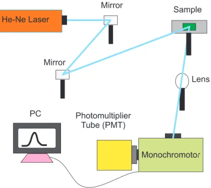
There are many process parameters that effect the luminescence spectrum of the PECVD grown Si-ncs. These effects can be listed as nanocrystal size and distribution, annealing temperature, time, and atmosphere. By using the PL set-up, given in the Figure 2.3, we have investigated these effects on Si-rich silicon oxide and nitride films.
Figure 2.3: Experimental set-up of the photoluminescence
The experimental setup that is used to take PL data uses the 632 nm line of a He-Ne laser or 514.5 nm or 488 nm of an Ar+ laser as the excitation source. The
CHAPTER 2. NANOCRYSTAL MOS CAPACITORS 16
sample is illuminated using a cylindrical lens for a line focus to minimize sample heating. Photoexcited luminescence is collected by a collection lens corrected for spherical aberrations and F number matched to a double monochromator. A GaAs based photomultiplier was used in the photon counting mode to record the data.
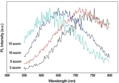
The luminescence intensity depends on the amount of excess Si concentration. Luminescence intensity is maximum for a concentration of Si in excess equal to 30% of the SiO2 concentration. When a larger concentration of Si is added,
the luminescence signal decreases with the Si concentration. The position of the luminescence peak also red shifts with increasing Si concentration as can be seen from Figure 2.4. 500 550 600 650 700 750 800 3 sccm 10 sccm P L In te n s it y (a .u .) Wavelength (nm) 15 sccm 5 sccm
Figure 2.4: Effect of Si concentration on the photoluminescence. Si rich silicon nitride films with varying NH3flow rates were investigated. Note that the redshift
in photoluminesce curve with increasing Si concentration.
The size of the Si-ncs were controlled by the flow rate of the NH3gas. Instead
of varying the flow rate of SiH4, we used a fixed SiH4 value of 350 sccm and
changed the flow rate of NH3 between 3 to 15 sccm. An increase in NH3 flow
rate can be considered as similar to a decrease in SiH4 flow rate. For 3 sccm of
NH3, the position of the PL peak was at about 750 nm, and this value decreased
to 600 nm when the concentration of the gas reached to 15 sccm. This means the size of the Si-ncs get smaller as the NH3 flow rates increase.
CHAPTER 2. NANOCRYSTAL MOS CAPACITORS 17
These observations can be understood within the quantum confinement model of nanocrystals since increasing Si concentrations (indicated by decreasing NH3
flow rates) lead to formation of larger nanocrystals. Energy separation between the bound states decreases as the nanocrystal size increases leading to red shift of the observed luminescence. For us, this is a signature for the presence of Si nanocrystals allowing us to optimize the growth conditions of the layers to be used in the MOS capacitor structures
On the other hand, the Si-nc formation mechanism in SiO2 matrix layer
requires a thermal activation temperature greater than 900 oC which is stated
by Li et al [26]. This feature suggests a growth mechanism which promotes the clustering of small Si-nc into larger Si-nc under high temperature annealing. This process is called Ostwald ripening, which is a spontaneous process that occurs because larger crystals are more energetically favored than smaller crystals. This mechanism proposes that the smaller sized Si clusters act as a source for the bigger sized clusters. As a result, disappearance of small Si clusters leads to the formation of larger sized Si nanocrystals.
Moreover annealing at high temperature can eliminate most of the defects that are formed during growth mechanism. The luminescence intensity grows as the annealing time increases and also large Si-ncs can be formed by increasing the annealing time. The annealing temperature and time were scanned for Si-ncs in silicon dioxide matrix. The results are given in Figure 2.5.
The Si-rich silicon dioxide films in Figure 2.5 were prepared using 200 sccm of
SiH4 and 8 sccm of N2O at 350 oC. The minimum PL signal was obtained from
as grown films as expected. For 1200 oC the PL peak shifted toward the lower
photon energies which is a direct result of clustering of small Si-ncs into larger Si-ncs. The annealing time slightly changed the PL spectrum. For the samples that were annealed at 1100 oC, 2 hours of annealing resulted in a redshift in the
PL which supports the formation of large Si-ncs by increased annealing time. The optimum temperature and time were obtained as 1200oC and 1 hour, respectively
for Si-rich silicon dioxide films.
CHAPTER 2. NANOCRYSTAL MOS CAPACITORS 18 500 550 600 650 700 750 800 850 0 3000 6000 9000 12000 15000 1100 oC, 2hours P L In te n s it y (a .u .) l (nm) 1200 oC, 1hour 1100 oC, 1hour as grown
Figure 2.5: Effect of annealing temperature and time on the photoluminescence. Annealed and unannealed Si rich silicon dioxide films were used for this experi-ment. The PL curve is maximum for 1200 oC and 1 hour annealing conditions.
the shape and the intensity of the luminescence emission spectra [50]. The ambi-ent gas during annealing can be used for passivation of the samples. In hydrogen environment, luminescence can increase by as much as one order of magnitude (11). This increase in luminescence is attributed to the termination of dangling bonds by hydrogen atoms which are responsible for non-radiative recombination. Passivation can also induce a blueshift or a redshift of the PL spectrum. This data is indicative of the presence of Si nanocrystals and their size which is important in the design and fabrication of Si nanocrystal based MOS capacitors.
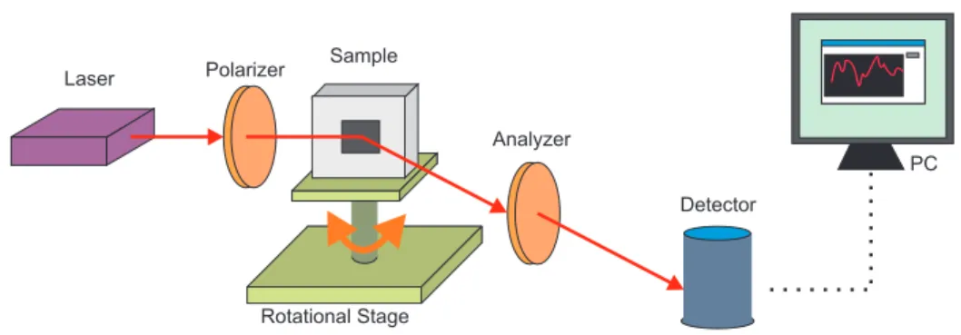
Optical ellipsometry was used to determine the optical properties (refractive index and extinction coefficient) of Si-ncs layers in the wavelength range from 400 to 1000 nm. The experimental set-up is given in Figure 2.6.
The ellipsometer is a commercial device made by Wollam Inc. It is a variable angle spectroscopic device capable of taking data in a wide range of incidence angles as well as wavelengths.
CHAPTER 2. NANOCRYSTAL MOS CAPACITORS 19 Laser Polarizer Analyzer Detector PC Sample Rotational Stage
Figure 2.6: Set-up for ellipsometry measurements.
Tauc-Lorentz dispersion model was used to describe the Si-ncs optical proper-ties. It is based on the determination of the imaginary part, ²2 , of the dielectric
function. The energy dependence of ²2 is modeled as the product of the Tauc
joint density of states with a Lorentz oscillator [3]:
²2(E) = 1 E AE0C(E−Eg)2 (E2−E2 0)+C2E2 f orE > Eg 0 otherwise (2.1)
In this formula, only one oscillator is used. The parameters A, C, E0represent
the amplitude and broadening of the oscillator and the peak transition energy, respectively. Eg is the optical band gap. The real part of the dielectric function
²1 is obtained by Kramers Kronig integration of ²2.
For ellipsometric measurements, two sets of samples were prepared, one with Si-rich silicon nitride and one with Si-rich silicon dioxide films. The optimum sample thickness was determined as 250 nm to obtain a reasonably high PL intensity and to avoid interference effects in ellipsometric measurements. The effect of PECVD gas flow rates and annealing temperatures on optical properties were studied by scanning each parameter.
Before ellipsometric studies, PL measurements were conducted, and the sam-ple that did not show any luminescence effect, was not considered for ellipsometric measurements so that, the number of parameters were limited. The Si-rich silicon dioxide films in Figure 2.6 were prepared using 200 sccm of SiH4 and 8 sccm of
CHAPTER 2. NANOCRYSTAL MOS CAPACITORS 20
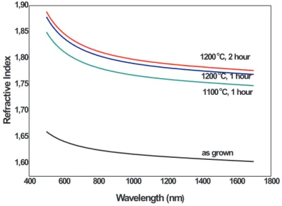
as 2.0 in the UV was obtained for rich nitride films, and 1.8 for annealed Si-rich oxide films. For comparison, the refractive index of what is considered as the stoichiometric silicon dioxide and silicon nitride films were also measured and refractive index values of 1.45 for silicon dioxide and 1.7 for silicon nitride films were obtained at 800 nm. The change in refractive index of Si-rich oxide films with annealing temperature and time is given in Figure 2.7.
400 600 800 1000 1200 1400 1600 1800 1,60 1,65 1,70 1,75 1,80 1,85 1,90 1100oC, 1 hour 1200oC, 2 hour 1200oC, 1 hour R e fr a c ti v e In d e x Wavelength(nm) as grown
Figure 2.7: Ellipsometric study of Si-rich SiO2 films with varying annealing
tem-peratures and times.
The refractive index of the unannealed sample was obtained as 1.62 at 800 nm. This value increased with the increasing annealing temperature and reached to 1.81 for annealing at 1200 oC for 2 hours. High temperature annealing triggers
the phase separation between Si and SiO2 and resulted in larger nanocrystal
formation. What was earlier a mixed matrix of SiO2 laced with Si atoms is now
SiO2 with clusters of Si nanocrystals. The sample that was annealed at 1200 oC
for 2 hours had the highest refractive index value of 1.81. The effect of annealing time become insignificant beyond a critical value, which may be considered as the saturation of the phase separation between Si and SiO2. Again, the results of
ellipsometric studies are indicative of the formation of Si nanocrystals and allows us to determine the growth conditions for the formation of Si nanocrystals.
CHAPTER 2. NANOCRYSTAL MOS CAPACITORS 21
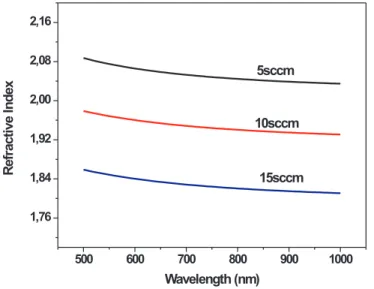
sccm of SiH4 and varying flow rates of NH3 between 5 to 10 sccm were studied
using ellipsometry, and the refractive index change as a function of the wavelength is given in Figure 2.8 500 600 700 800 900 1000 1,76 1,84 1,92 2,00 2,08 2,16 R e fr a c ti v e In d e x Wavelength (nm) 15sccm 10sccm 5sccm
Figure 2.8: Refractive index values of Si-rich silicon nitride film between 500 and 1000 nm.
2.2.3
Fabrication of Nanocrystal MOS Capacitors
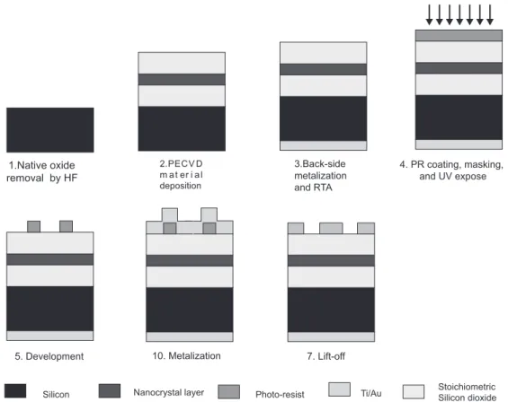
The memory devices used in this study were MOS capacitors with a trilayer dielectric stack consisting of Si/Ge nanocrystals sandwiched between a tunneling and a capping SiO2 layers. The n and p-type Si substrates with a resistivity of
1-10 Ωcm were cleaned by Piranha process followed by dipping in dilute HF for 1 min to remove the native oxide from the surface. Back side metalization was done by 10 nm of Titanium (Ti) and 50 nm of gold (Au) evaporation. To have a high quality ohmic contact, samples were subjected to rapid thermal annealing (RTA) in forming gas (5 % H2and 95 % N2) at 500oC for an optimized annealing time of
60 s. Then, a tunneling oxide layer of thickness 4 nm was grown on Si substrate by dry oxidation. The intermediate layer, containing of Si-ncs or Ge-ncs, was then deposited by PECVD method as explained previously. The thickness of the nanocrystal layer was 10 nm. The Si-rich silicondioxide and germanosilicate
CHAPTER 2. NANOCRYSTAL MOS CAPACITORS 22
samples were then annealed in N2 atmosphere in an alumina oven at 1200 oC
for 1 hour and between 650-850 oC for 5 minutes, respectively. Finally, the top
oxide layer (20-25 nm thick) was deposited by PECVD method. After defining the 1x1 mm capacitors by optical lithography, front side ohmic metalization was done by 10 nm of Ti and 50 nm of Au evaporation. As a last step, the samples were put into acetone solvent for lift-off process. The fabrication steps are given Figure 2.9. 1.Native oxide removal by HF 2.PECV D m a t er i a l deposition 4. PR coating, masking, and UV expose
5. Development 10. Metalization 7. Lift-off
Stoichiometric Silicon dioxide
Silicon Nanocrystal layer Photo-resist Ti/Au
3.Back-side metalization and RTA
Figure 2.9: Nanocrystal MOS fabrication fabrication steps.
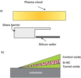
In samples where it was desired to obtain a well controlled thickness gradient, during PECVD material growth process, a glass barrier was placed over the silicon substrate. This procedure was not applied to all samples, but for some of them to observe the effect of film thickness on the storage and escape of electrons and holes. Using this method, device optimization can be made very quickly for PECVD grown devices. Schematic representation of this growth method is given in Figure 2.10.
CHAPTER 2. NANOCRYSTAL MOS CAPACITORS 23 Plasma cloud Glass barrier a) b) Si NC Tunnel oxide substrate Control oxide Silicon wafer
Figure 2.10: (a) A glass barrier is placed over a part of the silicon substrate for shielding the plasma. Under this barrier no material growth is observed. (b) This figure illustrates the structure of the sample after PECVD gradient growth method.
Chapter 3
Modelling of Nanocrystal MOS
Capacitors
3.1
Fundametals of MOS Capacitors
The nanocrystal memories that we have produced were basically metal-oxide-semiconductor (MOS) capacitors. To understand the operation mechanism of the nanocrystal flash memories, one has to know the operation mechanism of MOS capacitors. A typical MOS structure with silicon nanocrystal floating gate is given in Figure 3.1.
There are four different modes of operation for a MOS structure which are accumulation, depletion, flat-band, and inversion.
Accumulation
Accumulation occurs when a voltage less than the flat-band voltage,VF B, is
applied. The negative charges on the gate attracts holes from the substrate to the oxide-semiconductor interface. In the case of nanocrystal floating gate MOS capacitors, the electrons inside the nanocrystals are detrapped and holes are accumulated. Only a small amount of band bending is needed to build up the
CHAPTER 3. MODELLING OF NANOCRYSTAL MOS CAPACITORS 25 Si substrate Tunnel oxide Si-rich oxide Si-ncs Control oxide V+ V-Electrode Gate Electrode
Figure 3.1: A MOS capacitor structure with Si-ncs are used as floating gate.
accumulation charge. The schematic illustration of charge transport and band-diagram during the accumulation operation of Si-nc MOS capacitors is given in Figure 3.2.
Depletion
Depletion occurs for positive voltages. When a positive voltage is applied to the gate, the holes in the semiconductor close to the gate are repelled by the positive charge on the gate, and they exit the device from bottom contact. They leave behind a depleted region which is insulating due to the absence of mobile carriers. The depletion layer width further increases with increasing gate voltage until oxide breakdown occurs.
Deep depletion refers to widening of the depletion layer beyond its thermal equilibrium width. Deep depletion can also occur in thin oxide MOS capacitors, with oxide thickness less than 5 nm. In such devices an inversion layer cannot form because minority carriers tunnel through the oxide to the gate electrode and consequently, deep depletion occurs.
CHAPTER 3. MODELLING OF NANOCRYSTAL MOS CAPACITORS 26 Si substrate Tunnel oxide Si-rich oxide Si-ncs Control oxide V-V+ Electrode Gate Electrode Electron detrapping a) Metal gate Gate oxide Ec Ei Ef Ev
Nanocrystals Accumulation layer of holes
P-Si Vg<<0
Tunnel oxide
b)
Figure 3.2: a)During accumulation, electrons detrapped from nanocrystals with the applied positive gate voltage.b)
Inversion occurs at voltages beyond the threshold voltage. Negative charges inside the substrate are attracted by the positive gate voltage and a negatively charged inversion layer at the oxide-semiconductor interface is formed. In the case of Si-nc MOS structures, electrons are trapped inside the nanocrystals. The schematic representation of charge transport and band diagram during the inver-sion operation of nanocrystal MOS capacitors is given in Figure 3.3
Flat-band
When there is no charge in the semiconductor, the energy band diagram be-comes flat, this is referred as flat-band. The voltage separating the accumulation and depletion regime is called as flat-band voltage, VF B. The flat band voltage
is obtained when the applied gate voltage equals the work-function difference be-tween the gate metal and the semiconductor. If there is also a fixed charge in the oxide and/or at the oxide-silicon interface, the expression for the flat-band voltage must be modified accordingly.
CHAPTER 3. MODELLING OF NANOCRYSTAL MOS CAPACITORS 27 Metal gate Gate oxide Ec Ei Ef Ev Nanocrystals Tunnel oxide
Inversion layer of electrons Depletion layer P-Si Vg>>0 Si substrate Tunnel oxide Si-rich oxide Si-ncs Control oxide V+ V-Electrode Gate Electrode Electron trapping b) a)
Figure 3.3: During inversion electrons trapped inside the nanocrystals by applying negative positive voltage to the gate electrode.
3.2
Basic Conduction Mechanisms for MOS
Ca-pacitors
Most amorphous insulators under an electric field show a range of nonlinear current-voltage dependence, and can be interpreted based on certain conduction mechanisms. The fundamental mechanisms in the description of the current-voltage (I-V) characteristics of a MOS structure are Fowler-Nordheim (FN) and direct tunneling.
Fowler-Nordheim Tunneling
FN tunneling has been studied extensively in MOS structures where it has been shown to be the dominant current mechanism, especially for thick oxides (> 4 nm)) [42]. The basic idea is that quantum tunneling of carriers occurs through a triangular potential barrier in the presence of a high electric field as shown in Figure 3.4.
The barrier of the insulator is pulled down by the electric field and as a result electron tunneling from the metal Fermi level into the oxide conduction band
CHAPTER 3. MODELLING OF NANOCRYSTAL MOS CAPACITORS 28
Direct Tunneling
a)
b)
Figure 3.4: Schematic representation of the Fowler Nordheim tunneling under high voltage. In here ΦB barrier height, EF M metal Fermi level, EF S
semicon-ductor Fermi level, dox oxide thickness, dF N tunneling distance, and Vgate gate
voltage
becomes possible. To check whether the leading current mechanism in the device is FN tunneling, I-V data is typically plotted as ln(JF N/Eox2 ) - 1/Eox, a so-called
Fowler-Nordheim plot. FN tunneling is worked under high electric field, therefore using the FN tunneling to in charge/discharge operations will result in defects or carrier accumulation, and eventually breakdown occurs [42].
Direct Tunneling
In the simple case for oxide thickness smaller than 2 nm, direct tunneling dominates, the electrons pass through the full oxide thickness and the gate current is due to direct tunneling [19]. The graphical representation of direct tunneling mechanism and corresponding band diagram is given in Figure 3.4.
Direct-tunneling regime enables fast and low voltage operations but is limited by charge loss in the continuous floating gate. The probability of direct tunneling is a very strong function of the width of the barrier that electron tunnels through (oxide thickness in MOS devices).
CHAPTER 3. MODELLING OF NANOCRYSTAL MOS CAPACITORS 29
3.3
Fundamentals of Nanocrystal MOS
capaci-tor
In [27], it is assumed that, only nanocrystals are responsible for charge/storage and a single electron is stored in a nanocrystal. Based on these assumptions flat-band voltage shift can be written as:
∆VF B = qnnc ²ox (tox+ ²oxtnc 2²ge ) ' qnnctox ²ox (3.1)
where q is the electronic charge, tox is the total oxide thickness including
control and tunnel oxides, tnc is the average diameter of the nanocrystals, ²’s are
the dielectric constants of respective materials.
To understand dynamical properties of memory elements, charging and dis-charging currents must be calculated taking into account tunnelling through the barrier for a given electric field within the tunnelling region. The currents also depend on availability of initial and final states. Since there are many device parameters that determine the charge-discharge currents, obtaining an analyti-cal formula is difficult. Therefore, in the following charge, discharge and erase currents are studied separately, and appropriate formulas are given whenever possible.
3.3.1
Charging of Nanocrystal MOS capacitors
We try to model charging with the simplest approach. During the write cycle, the device is in accumulation and initially there is no stored charge in the device. In this case, the oxide field Ftox will be determined by the gate voltage Vgate
approximately as Ftox ' Vgate/tox, where tox is the total oxide thickness.
For calculating the tunnelling current through a trapezoidal barrier, two limits in terms of applied field can be used. High-field limit is occurred when the voltage drop across the barrier is greater than the unperturbed barrier height. This results
CHAPTER 3. MODELLING OF NANOCRYSTAL MOS CAPACITORS 30
in the well known Fowler-Nordheim current. When the tunneling oxide is very thin, the direct tunnelling limit is observed. In direct tunneling the voltage drop across the barrier is smaller than the original barrier height. Since, low voltage operation is desired in flash memory devices, we assume low fields and calculate direct tunnelling currents for the charging case. In this case, the charging current density becomes [17].
Jc=
AF2
tox
VB
× exp[−(1 − (1 −Ftoxttox VB )3/2)BV 3/2 B Ftox ] (3.2) where A = q2m si/16π2mox¯h, B = 2 √
8moxq/3¯h, Ftox is the tunnel oxide field
during charging, mox is the tunnel effective mass and VB is the barrier height
between the oxide and the substrate.
The availability of the final states will determine the deposited actual charge. Using a capture cross section per nanocrystal, this problem can be solved. The differential charge deposited per unit area dσ in a time interval dτ can be calcu-lated as:
dσ = pcDtrapJc(Ftox)dτ (3.3)
where pcis the average capture cross section, and Dtrapis the available density
of final states. The capture probability may depend on nanocrystal shape.
3.3.2
Discharging of Nanocrystal MOS Capacitors
During retention, the device is in depletion and Vgate = 0. If we assume that
the nanocrystal bound states are responsible for storage of carriers, the discharge of the electrons occurs by tunnelling from the nanocrystal ground state to the substrate, either by direct or trap assisted tunnelling. For the case of direct tunnelling, the current density describing the discharge of the nanocrystals is different than Eq. 3.2 because initial states are nanocrystal states instead of
CHAPTER 3. MODELLING OF NANOCRYSTAL MOS CAPACITORS 31
bulk states. Assuming a delta-function distribution for the nanocrystal states
DN C(E) = NN Cδ(E − EN C) located at the quantization energy of EN C and a
single stored carrier for every nanocrystal, the discharge current density can be given as
Jd= qNN CTt(ENC)νN C (3.4)
where νN C ' ¯hπ/2mged2 is the semi-classical escape attempt rate for NCs of
diameter d [36].
The transmission probability Tt(E, Ftox) for a single electron at energy E can
be calculated through the WKB approximation as
Tt(E) ≈ 4 exp[−(1 − (1 − Ftoxttox
VB(E)
)3/2)BVB(E)
3/2
Ftox
]. (3.5)
The tunnel oxide field is determined by the amount of stored carriers as well as by the band-bending. For a given stored charge, the oxide field depends on the tunnel oxide thickness, total oxide thickness, substrate doping, gate work-function and dielectric constants. In order to obtain an appropriate result, we consider the case where stored charge is small and tunnel oxide field is proportional to the stored charge , Ftox≈ ∆VF B/2tox.
For the calculation of the discharge current through Eqs. 3.4 and 3.5, the barrier height must also be calculated. The barrier height is a function of the nanocrystal ground state energy given by VB(E) = VB0− EN C, where VB0 is the
bulk barrier height. The conduction band minimum of Ge NCs as a function of size is given by [35]
ECBM(d) = ECBM(∞) +
11.86
d2+ 1.51d + 3.3936 (3.6)
CHAPTER 3. MODELLING OF NANOCRYSTAL MOS CAPACITORS 32
can be used to estimate EN C, which can be used in the estimation the tunnelling
barrier observed by the nanocrystals during discharge.
The size distribution of nanocrystals leads to a distribution of energies. Con-sidering the finite width of size distribution, using a broadened density of states is more appropriate than using delta function distribution. In this case, the stored charge is distributed to the available nanocrystal states according to a Fermi-Dirac distribution.
Assuming thermal equilibrium within the nanocrystal layer, the distribution of carriers to available states and the quasi-Fermi level can be calculated for a given total stored charge. In this case, for a given total areal density of NN C, the
total number of stored carriers is given by
nc= NN C √ 2πσE Z exp[−(E − E N C,ave)2/2σE2] 1 + exp[(E − EF,N C)/kBT ] dE (3.7)
where EN C,ave is the average nanocrystal ground state energy, EF,N C is the
quasi-Fermi level of the nanocrystals layer, and σE is the half-width of the
nanocrystals energy distribution.
The quasi-Fermi level is a weak function of temperature, but depends strongly only on the ratio of total stored charge to number of nanocrystals. Therefore, for a given flat-band voltage shift, the quasi-Fermi level depends on the nanocrystal density, and average ground state energy of the nanocrystals. Escape of carriers near or above the quasi-Fermi level dominates the discharge current. Therefore, discharge current depends on the number of stored carriers which is proportional to the flat-band voltage shift.
A simple formula for the discharge current is desirable to compare the ef-fect of design parameters on charge retention. However, simple expression for the quasi-Fermi level and tunnelling current can not be obtained without fur-ther simplifying assumptions. A simple formula can be obtained by assuming a rectangular shaped density of states, neglecting band bending effects, assuming a gate work-function that is aligned with the substrate Fermi level and calculating