On-chip integrated nanowire devices with controllable nanogap for
manipulation, capturing, and electrical characterization of nanoparticles
Can Uran1, 3, 4, Emre Unal3, 4, Ramazan Kizil5, and Hilmi Volkan Demir1,2, 3, 4,*
1Department of Electrical and Electronics Engineering, 2Department of Physics, 3Nanotechnology Research Center, 4Institute of Materials
Science and Nanotechnology, Bilkent University, Bilkent, Ankara 06800 Turkey
5Department of Chemical Engineering, Istanbul Technical University, Istanbul 34469, Turkey
*Tel:[+90]( 312) 290 1021, e-mail: [email protected]
Dielectrophoresis (DEP) allows for electric field assisted assembly in spatially non-uniform field distribution, where the induced moment is translated into a net force on polarized particles towards the high field gradient. For example, for a spherical particle of radius r with a permittivity constant of εp in a host medium with the
permittivity of εm, the dielectrophoretic force is given by (1):
[
]
rmsm
DEP r K E
F =2
π
3ε
Re (ω
)∇ 2 (1)where r is the particle radius, ω is the angular frequency and Erms is the root mean square electric field. K(ω) is
the Clausius-Mossotti function, which depends on the complex permittivity of the spherical particle and the medium [1].
We present a nanoscale device platform constructed with dielectrophoretic self-assembly of our segmented nanowires. These aligned nanowires automatically provide electrical contacts to the captured nanoparticles to allow for electrical probing at the nanoscale. This enables full integration from nanoparticles to nanowires to microelectrodes to macroprobes on a single chip, spanning a size range of more than six orders of magnitude. For processing, we first pattern the bottom metal layer made of Au (bottom electrodes) that provides an electrical path to upper electrodes through AC coupling. We subsequently deposit a silicon nitride layer, which serves as the dielectric layer for capacitive coupling between the lower electrodes and the upper electrodes, and finally pattern the upper gold microelectrodes. The dielectric layer prevents electrical shortage of these electrodes to metallic nanowires during the assembly process and enables characterization of each nanowire individually. The separation between the tips of the second layer (upper) electrodes fingers are designed to be 5-6 µm long, where the nanowires align at the highest field gradient.
Using electrodeposition, we synthesize Au-Ag-Au segmented nanowires in porous membranes made of aluminum oxide (Whatman Anodisc) used as the template. We start the deposition of the gold segment using a current level of 1.6 mA at a deposition rate of 60 nm/min while the reduction occurs for a potential range of -1.70 V and -2.65 V. For subsequent Ag segment that determines the size of our gap, we employ a constant current level of -1.6 mA while varying deposition times to make Ag segments of varying lengths tuned from 300 nm down to 20 nm. Our rate of silver deposition is 85 nm/min for a potential range of -1.40 V and -1.70 V. After aligning Au-Ag-Au nanowires, their middle Ag segments are removed chemically etching Ag with dilute nitric acid (HNO3) solution and/or by post-baking process at 200°C for 75 min. This allows for the two ends of
the nanowires to be automatically and precisely aligned. Thermal baking enables us to smoothen the nonuniform morphology of the nanogaps, and strengthens the electrical contacts of the gold segment ends of the nanowires to the microelectrodes [2].
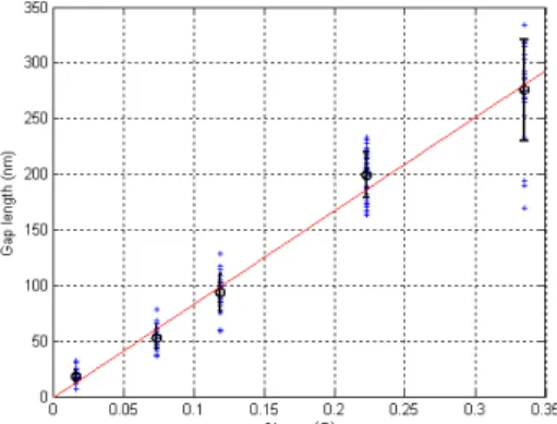
Fig. 1 shows different lengths of Ag segments. The length of these Ag segments is linearly proportional to the total charge driven into the pores of the membrane during electrodeposition, and the deposition time of silver, which conveniently allows for controlling the lengths of Ag segments as we use constant current. We form a nanogap with a size equal to the size of our Ag segment after the Ag segment is selectively etched.
We also synthesize narrow nanowires with high aspect ratio in track-etched polycarbonate membranes, which have diameters <40 nm with the goal of capturing single nanoparticles to capture and characterize. It is very challenging to fabricate such nanowire structures with e-beam lithography (EBL) and focused ion beam (FIB) technology. The in-template NW synthesis is also a highly parallel and cheap process, enabling the synthesis of our nanowires in massive number.
Using DEP, we align our nanowires, which are dispersed randomly in liquid medium on the pre-fabricated microelectrode arrays with the purpose of single nanowire alignment across each of the electrode pairs in the array. After dielectrophoretic alignment of these nanowires on the electrode arrays, we obtain a three-dimensional suspended air-bridge architecture across a pair of electrodes (Fig. 2). Standard nanofabrication of such a suspended structure is very demanding at these dimensions.
217
TuK4
11.30 - 11.45
Figure 2. Suspended nano-bridge architecture achieved by dielectrophoresis of the nanowire on electrodes.
We observe the effects of frequency, voltage and nanowire concentration parameters on DEP experiments. The resulting dielectrophoretic force is strong for Au-Ag-Au nanowires in methanol at 10 kHz, and electric field of ~105 eV needs to be applied across the fingers to achieve required dielectrophoretic force on nanowires. We use
a reasonable nanowire concentration of 2.5x10⁷ ml-1, which reproducibly achieves high yield alignments more
than %20.
Using DEP for the second time, we capture gold nanoparticles at the nanogaps by applying sinusoidal waveform with Vpp of 10 V at 1 MHz across primary pads in aqueous solution. Furthermore, we successfully capture
cadmium selenide/zinc sulfide (CdSe/ZnS) nanocrystals in toluene with diameters of ~20 nm, with the help of ultra-violet (UV) illumination at an optical wavelength of 254 nm increasing nanocrystal polarizability by photogenerating electron-hole pairs inside them.
In Fig. 3(a)-(d), we show our proof-of-concept demonstration of the nanowire platform integrated with microelectrodes by I-V measurements and SEM imaging in each step of the integration. First, we observe electrical conductance through the Au-Ag-Au NW by probing the microelectrodes, which the two Au ends are in contact (shown in the inset of Fig. 3(b)). However, after the removal of middle section, we observe the open circuit behavior, confirming the formation of a nanogap (shown in the inset of Fig. 3(c)). Finally, after capturing nanoparticles in the gap, we observe strong electrical conduction again across the electrodes (shown in the inset of Fig. 3(d)), when metal nanoparticles bridge the gap implying that our on-chip nanowire device platform is convenient for nanoparticle capturing and their electrical characterization [3].
In summary, we reported on nanowire device platforms that are fabricated by aligning segmented (Au-Ag-Au) nanowires across microelectrode arrays under AC-electric-field and controllably forming nanogaps via selectively removing the middle (Ag) segment. This platform holds great promise to capture and probe nanoparticles.
Acknowledgements: This work is supported by EU MOON, EU NOE PHOREMOST and TUBITAK 104E114, 106E020, 107E088, 107E297, 109E002, 105E065, and 105E066. H.V.D. also acknowledges additional support from Turkish Academy of Sciences (TUBA GEBIP) and European Science Foundation (ESF-EURYI).
References
[1] H. A. Pohl, Dielectrophoresis-The behavior of neutral matter in nonuniform electric fields, Cambridge Uni. Press (1978). [2] S. Liu, J. B.-H. Tok, and Z. Bao Nano Lett., Vol. 5, 1071-1076 (2003).
[3] C. Uran, et al., IEEE J. Special Topics in Quantum Electronics, 2020057 (2009).
Figure 1.Gap length vs. injected charge in electrodeposition. (Plus signs represent the lengths of Ag segments, and error bars represent the standard deviation across Ag segment lengths.)
Figure 3. SEM images of (a) microelectrode fingers before nanowire alignment showing open circuit I-V characteristics in the inset, (b) aligned Au-Ag-Au segmented nanowire by using DEP and clamps showing electrical conduction in the inset, (c) nanowire after gap formation in the middle showing open circuit again in the inset), and finally (d) nanoparticles captured in the size controllable nanogap by using DEP showing electrical conduction in the inset).