IMPLEMENTATION OF HIGH
QUALITY-FACTOR ON-CHIP TUNED MICROWAVE
RESONATORS AT 7 GHz
Rohat Melik1,2and Hilmi Volkan Demir1,2 1Department of Electrical and Electronics Engineering,
Nanotechnology Research Center, and Institute of Materials Science and Nanotechnology, Bilkent University, Ankara 06800, Turkey 2Department of Physics, Nanotechnology Research Center, and Institute of Materials Science and Nanotechnology, Bilkent University, Ankara 06800, Turkey; Corresponding author: [email protected]
Received 20 June 2008
ABSTRACT: We report on the design, analytical modeling, numerical
simulation, fabrication, and experimental characterization of chip-scale microwave resonators that exhibit high quality-factors (Q-factors) in the microwave frequency range. We demonstrate high Q-factors by tuning these microwave resonators with the film capacitance of their LC tank circuits rather than the conventional approach of using external capaci-tors for tuning. Our chip-scale resonator design further minimizes en-ergy losses and reduces the effect of skin depth leading to high Q-fac-tors even for significantly reduced device areas. Using our new design methodology, we observe that despite the higher resonance frequency and smaller chip size, the Q-factor is improved compared with the pre-vious literature using traditional approaches. For our 540m ⫻ 540
m resonator chip, we theoretically compute a Q-factor of 52.40 at the
calculated resonance frequency of 6.70 GHz and experimentally demon-strate a Q-factor of 47.10 at the measured resonance frequency of 6.97 GHz. We thus achieve optimal design for microwave resonators with the highest Q-factor in the smallest space for operation at 6.97 GHz. © 2008
Wiley Periodicals, Inc. Microwave Opt Technol Lett 51: 497–501, 2009; Published online in Wiley InterScience (www.interscience.wiley.com). DOI 10.1002/mop.24103
Key words: microwave; resonators; quality-factor; tuning; fabrication 1. INTRODUCTION
High quality-factor (Q-factor) resonators are required for good performance in applications such as microwave devices, mobile phones, radars, wireless universal serial buses (USB), and wireless local area networks (WLAN). In such applications, on-chip reso-nators are preferred because they reduce power consumption, prevent connection losses, and facilitate on-chip integration. These lead to compact, low-cost systems. However, it is difficult to produce chip-scale, small-size resonators that exhibit high Q-factors at high frequencies. In general, smaller resonators yield lower Q-factors. To date, microwave resonators based on on-chip spiral coils have been successfully demonstrated, with unloaded
Q-factors of inductors up to a maximum of 40 at 5 GHz [1] and 50
at 2 GHz [2], which would further be reduced for operation at higher frequencies [1, 2]. In these studies, to realize resonators using these inductors, external capacitors are used to tune the inductors, which undesirably increase the effective device area and decrease the resonator Q-factor. The use of such an externally connected capacitor further results in longer propagation times and fewer operating channels for communication. It has also previ-ously been shown that higher Q-factors can be achieved using cavity geometries. But this then comes at the cost of significantly increased size, resulting in much larger chips (as long as several millimeters on one side) [3] and in more complicated fabrication steps. Therefore, these are not ideal methods to obtain a compact and high Q-factor microwave resonator operating at a high fre-quency. In addition to the need for a high-frequency, high-Q resonator, there is a strong demand for bio-implant resonators in medical applications that would satisfy the biocompatibility
con-straints [4]. In this work, with the motivation to address the need for compact high-Q bioimplantable microwave resonators, we develop and demonstrate on-chip biocompatible resonators with high Q-factors of about 50 in the microwave frequency range, despite their chip-scale, small size (sub-millimeter on one side).
In the literature, Q-factors are typically stated in unloaded cases, excluding the external loading effects [5, 6]. In this article, we report the measured Q-factors including the loading effects and the associated losses instead of merely citing unloaded Q-factors. Thus, we present the worst case Q-factor values, with the probe loading and related losses all included. Furthermore, we imple-ment the resonator aiming for a minimal device size while oper-ating with a high Q-factor at a high frequency. To do so, we develop a new design methodology that reduces the effect of skin depth in attaining high Q-factors. In our device, although the metal layer is very thin, we can achieve high Q-factors because of our new design approach. The area of our microwave resonator is
demonstrated to be as small as 540 m ⫻ 540 m while the
Q-factor is still kept high at 47.10, which is not possible with
previous approaches in the literature.
The resonator architecture is based on a spiral coil structure with a few turns tuned with the on-chip capacitance to obtain the highest Q-factor from the smallest lateral chip size. This approach relies on minimizing energy losses in the coil and also on using the film capacitance for tuning. We develop a two-port circuit model design for our on-chip coil. We support our analytical model with numerical simulations. Our analytical model obtains targeted res-onance frequencies that are very close to the resres-onance frequencies we obtained with numerical simulations and those that are later measured experimentally on our fabricated chips.
Although we implement our resonator chips using a standard microelectro-mechanical-systems (MEMS) fabrication procedure, we design them to be compatible with complementary metal oxide semiconductor (CMOS) processing, while also using only biocom-patible materials. Our resonators are of a size (a half millimeter by a half millimeter with 100 nm thick metal lines) to possibly be fabricated in large quantities, at a low per-unit cost, by standard CMOS processes and conveniently be integrated on-chip with CMOS electronics.
In this article, we present the design, analytical modeling, numerical simulation, fabrication, and experimental characteriza-tion of such compact high-Q microwave resonators. The rest of this article is organized accordingly as follows. We first present the theoretical background in Section 2 and then describe the micro-fabrication of our on-chip resonators and their experimental char-acterization along with our theoretical analysis in Section 3 and finally conclude in Section 4.
2. THEORETICAL BACKGROUND
We develop our circuit model for a spiral coil starting with the circuit model of a general transmission line [7]. We consider the coil as being composed of many transmission line segments in serial connection [8]. For each of these transmission lines, with half of their capacitance terminated both at the beginning and the end of each segment, we put together all of these transmission line segments and include the admittance to ground through the dielec-tric capacitance and substrate to construct the coil [9]. For further simplification, we convert this coil model into a conventional circuit that matches the coil structure. The circuit conversion is illustrated step by step from Figures 1(a)–1(c). In the literature, one of the ports is commonly taken as ground especially for the analysis of the measured S parameters, which significantly simpli-fies the analysis [10]. In our case, we produce the final circuit
model using two ports as shown in Figure 1(d). We perform all of our analytical modeling, analytical simulations, and designs based on this final two-port circuit model representation. The standard way of calculating a resonator Q-factor is based on measuring the 3-dB bandwidth ratio of S21magnitude [11], which is different from calculating an inductor Q-factor by measuring reflectivity after grounding one port of the circuit.
To calculate the circuit components for the coil model, we use the equations listed together for convenience in Table 1. These equations relate our structural design parameters to the circuit components of our coil resonator (and thus to the resonator spec-ifications). Our on-chip microwave resonator consists of metal layers (Au) that make up the spiral coil structure and the insulator layers (Si3N4) that isolate the metal layers from each other and the substrate (Si). In our circuit model, LS is the inductance of the spiral coil; Cfilm is the capacitance of the dielectric thin film between the coil and the substrate; CSiis the capacitance from the coil trace to the substrate for a half turn; CSis the capacitance between adjacent coil segments; RSiis the resistance of the sub-strate; and RSis the resistance of the spiral coil. Additionally, in Table 1, in the inductance Eq. (1), Lselfis the self-inductance, M⫹ and M⫺are the positive and negative mutual inductance, respec-tively; and in the coil resistance Eq. (6), ␦ is the skin depth. Moreover, device design parameters used in these equations in-clude the total length of the spiral coil (l), the metal width (w), the separation between metal lines (s), the dielectric thin film thickness (tfilm), the coil metal thickness (t), the total length and width of the resonator chip (LCand WC), and the number of turns (N).
In Table 1, the inductance parameters LS, Lself, M⫹, and M⫺are calculated [12]. For calculating CSiand RSi, experimental charac-terization results are used in the method given in Lee [13]. For RP and CP, the relations in Bahl [4] are utilized. We obtain RPand CP through the circuit conversion from Figures 1(b) and 1(c). Here RP and CPrepresent the combined impedances of RSi, CSi, and Cfilm.
RPis particularly important for the computation of substrate losses and CPis significant for the resonance frequency and the self-resonance factor.
Our design guidelines rely on the objective of maximizing
Q-factor of our on-chip microwave resonators. Thus, the Q-factor
definition is important. The Q-factor of a resonator is defined in the most general sense in Eq. (13) [14]:
Q⫽ 2 energy stored
energy loss in one oscillation cycle (13)
The empirical form of this Q-factor definition is presented in Eq. (12) in Table 1. However, this equation does not identify the lumped elements that store energy and those that dissipate energy.
Therefore, it does not provide guidance on how to increase the
Q-factor. For that reason, in our design methodology, we utilize
the definition of the Q-factor of the inductor (rather than the entire LC tank circuit of the resonator). We can obtain the resonator
Q-factor using both the inductor Q-factor (Qind) and capacitor Q-factor (Qc) as given in Ludwig and Bretchko [11]: 1
Qres
⫽ Q1
ind ⫹
1
Qc
. Structural design and material selection do not affect Qcvery much. However, Qind is directly affected by geo-metrical design and the material selection. As a result, we can maximize the resonator Q-factor by using the classical resonance definition and the methods to increase Qind. The inductor Q-factor
is given by Eqs. (14) and (15) [15].
Qind⫽ 2
peak magnetic energy⫺ peak electric energy
energy loss in one oscillation cycle (14)
Qind⫽ R L
冋
1⫺冉
o冊
2册
(15)The open form of this equation is presented in Eq. (10) in Table 1, which explicitly shows the design factors that affect the inductor
Q-factor (i.e., the elements that store energy and those that
dissi-pate energy). As shown in Eqs. (14) and (15), Qindis proportional to the difference between peak magnetic energy and peak electric energy, and the resonance frequency is the one where these two energies are equal, i.e., where the inductor’s Q-factor is zero. This is the point where the tank circuit has the minimum transmitted power. Equation (11) of Table 1 gives the basic definition of the
Figure 1 Our circuit model conversion: We first consider a source driving the conventional circuit of the coil with two ports in (a), then consider one of these ports to be grounded in (b), from which we obtain the common representation of a parallel RLC circuit in (c). Unlike other approaches, here we expand this model further into a simple two-port circuit representation in (d) to be used for all of our analytical simulations.
TABLE 1 List of Empirical Equations Used to Calculate Circuit Components from Design Parameters
LS ⫽ 兩 Lself兩 ⫹ 兩 M⫹兩 ⫺ 兩 M⫺兩 (1)
Cfilm ⫽ orlw
tfilm
(2)
CSi ⫽ 0.5lwCsub, where Csub ⫽ 1.6 ⫻ 10⫺10
F cm2 (3) CS ⫽ 0lt s (4) RSi ⫽ 2 lwGsub , where Gsub ⫽ 0.4 1 ⍀cm2 (5) RS ⫽ l w␦ ⫻ 共1 ⫺ e1␦兲 (6) ␦ ⫽
冑
2 0 , where ⫽ 2f (7) RP ⫽ 1 2C film 2 R Si ⫹ RSi共Cfilm⫹ CSi兲2 Cfilm2 (8) CP ⫽ Cfilm 1⫹2共C film⫹ CSi兲CSiRSi2 1⫹2共C film⫹ CSi兲2RSi2 (9) Qind ⫽ LS RS ⫻ 2RP 2RP⫹冋冉
LS RS冊
2 ⫹ 1册
RS ⫻冤
1 ⫺ RS2冉
CP 2⫹ CS冊
LS ⫺ 2L S冉
CP 2 ⫹ CS冊
冥
(10) f0 ⫽ 1 2冑
LC (11) Q ⫽ f0 ⌬f (12)resonance frequency f0, which corresponds to the point where Qind is zero and alternatively to the point where the transmitted power is minimum. When using the numerical or experimental data, we compute the resonance frequency from the point of minimum transmitted power. Because the device we fabricate is an on-chip resonator that does not require any tuning with an external capac-itor, we calculate the Q-factor theoretically as given in Eq. (12) of Table 1.
3. EXPERIMENTAL CHARACTERIZATION AND ANALYSIS
We design our devices to have a resonance frequency in the microwave frequency range in accordance with the criterion of maximum feasible Q-factor while maintaining the minimal size for targeted biomedical applications. To maximize the Q-factor of our microwave resonator, we construct our design methodology based on maximizing the inductor’s Q-factor. As discussed in Section 2,
Qindexplicitly includes the effect of design parameters on reso-nance and identifies the energy loss and storage elements. Given these guidelines, we set the device parameters. Table 2 summa-rizes two of our designs to demonstrate the effect of different design parameters for comparison purposes.
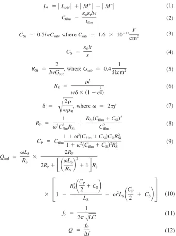
We use silicon as substrate and Au as metal layer as they are biocompatible (so that our resonator can be used as bio-MEMS sensors in future applications). We directly lay down the first metal layer used for contacts directly on the substrate to decrease sub-strate losses. We choose the Si3N4 thin film, which is also bio-compatible while featuring a low loss tangent (as low as 5⫻ 10⫺4) and a high dielectric constant (as high as 8) in the microwave frequency range. The low loss tangent significantly decreases the loss, whereas the high dielectric constant increases the dielectric film capacitance. To increase the resonance frequency and Qind and to make a compact resonator, we reduce the resonator chip area; LCand WCare thus as short as possible. By increasing the metal width (w), we decrease the sheet resistance and, hence, increase the Q-factor. An increase in the metal width with constant spacing between metal lines (s) increases the lateral area; we thus optimize the metal width and spacing, considering the Q-factor and compactness. The higher the metal spacing is, the lower the resonance frequency is. Generally, although smaller metal spacing increases Qind, one should also consider the effect of the ratio between w and s. This ratio should not be too large; otherwise, the parasitic capacitance eventually decreases Qind. The first design with 10m spacing features higher Qindbecause the w/s ratio of the other device is too large and thus the parasitic capacitance decreases the Q-factor.
In Figure 2, we show Qindcomputed for both designs (with s⫽
10 m and s ⫽ 5 m). Here, we observe that the maximum
inductor Q-factor of the first design with s⫽ 10m is higher than that of the second one with s⫽ 5m. At resonance frequencies, their inductor Q-factors cross the zero line; the first design with
s⫽ 10m has a resonance frequency of 6.70 GHz, and the second
design with s⫽ 5m has a resonance frequency of 7.00 GHz. High-Q factor in our designs is achieved because we use the capacitance of the dielectric thin film between the coil and the substrate for on-chip tuning and obtain an all on-chip, small-size microwave resonator. In fact, because we use the high dielectric capacitor instead of an external capacitor, the spiral inductor is
utilized the way that a cavity resonator would be. Thus, we obtain a high Q-factor, comparable to the results of cavity resonator studies, but here without sacrificing the small chip area. Therefore, this study effectively combines two different approaches: The spiral inductor concept and cavity resonator design techniques. In addition, considering the factors that reduce the losses and enhance the Q-factor by a careful inspection each of the circuit parameters in Figure 1(a), the losses are minimized and the Q-factor is maximized at a resonance frequency of 7 GHz. Also, if we further modify our resonator design to operate at even higher frequencies, the chip size becomes smaller and the Q-factor is enhanced be-cause of our design methodology, which is again different from the traditional approaches.
The first step in the fabrication procedure includes standard lithography and liftoff directly on a Si substrate to lay down the first metal layer made of Au with a thickness of 0.1m. We then deposit a Si3N4thin film using a plasma-enhanced chemical vapor deposition (PECVD) system; this film is 0.1m thick. To pattern the Si3N4film, we perform a second lithography to open vertical interconnection areas using a wet etching process with HF (hy-drofluoric acid). In the subsequent Au metallization step, we erect the interconnection layer. In the third lithography and Au metal-lization steps, we construct the top coil and contact pads and finally obtain our on-chip microwave resonator. Figure 4 summarizes our process flow to fabricate our devices and shows one of the fabri-cated devices. We characterize these fabrifabri-cated devices using a vector network analyzer (HP8510C). We calibrate our setup using
TABLE 2 Our Device Design Parameters
Design LC(m) WC(m) N w (m) s (m) tfilm(m) t (m)
1 540 540 2 100 10 0.1 0.1
2 520 520 2 100 5 0.1 0.1
Figure 2 Qindcomputed for our designs with s⫽ 10m and s ⫽ 5 m. [Color figure can be viewed in the online issue, which is available at www.interscience.wiley.com]
Figure 3 The process flow for the microfabrication of our on-chip microwave resonators shown in cross-sectional view at the stages of (a) metallization on the substrate, (b) dielectric film coating, (c) film patterning (wet etching), (d) interconnect metallization, and (e) final top coil metal-lization, along with (f) a top-view micrograph of our fabricated device. [Color figure can be viewed in the online issue, which is available at www.interscience.wiley.com]
the ISS (impedance standard substrate). In our measurements, we take 801 points and perform 128-point averaging both in calibra-tion and measurement.
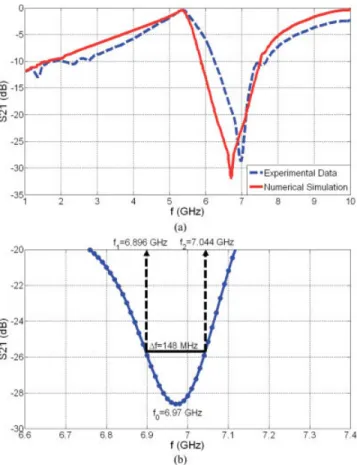
Figures 4 and 5 show the S21 parameters (in dB) that are experimentally measured and numerically simulated (in CST Mi-crowave Studio) together for our first and second designs (s⫽ 10 m and 5 m), respectively. We measure the Q-factors of the microwave resonators from the 3-dB bandwidth ratio of the S21 magnitude by taking transmission measurements [11]. Therefore, we obtain the loaded Q-factor including the external effects, which is different from calculating the Q-factor of an inductor alone by measuring reflectivity after grounding one port of the circuit. We observe sharp dips in the transmitted power at the resonance frequencies both in Figures 4(a) and 5(a). We measure the reso-nance frequencies (where S21is minimum) to be 6.97 and 7.12 GHz for our first and second designs, respectively. These experi-mental results match very well with the theoretical values of 6.70 and 7.00 GHz. Our theoretical and experimental results are sum-marized in Table 3.
To clearly illustrate 3-dB bandwidth measurements, Figures 4(b) and 5(b) depict the same experimental S21data presented in Figures 4(a) and 5(a), zooming in the resonance regions. As can be clearly seen in Figures 4(b) and 5(b), we measure⌬f of the first and second devices to be 148 and 178 MHz; these closely match the numerically calculated ⌬f values of 128 and 169 MHz, respec-tively. Using Eq. (12), we then experimentally obtain Q-factors for the first and second devices of 47.10 and 38.48; these are also in close agreement with the numerical results of 52.40 and 41.30, presented in Table 3.
Here, it is worth noting that we take all of our measurements loaded with standard microwave probes on the chips and then extract the Q-factors from these measurements in the loaded case including the losses coming from the probes. For example, for cavity resonators [5, 6], typically unloaded Q-factors are cited; these are calculated using the relation 1
Ql ⫽ 1 Qu ⫹ 1 Qe , where Qu is the unloaded Q-factor, Qlis the loaded Q-factor, and Qeis the external Q-factor. In these works, Quand Qeare larger than Ql. In
our case, we obtain and cite only the loaded Q-factors (Ql) in our experiments by placing the microwave probes on the chips and measuring the S21parameters with the probes. In our experimental characterization, the minimum point of this S21measurement gives
the resonance frequency f0; the points that are 3 dB above this minimum point give the 3-dB frequencies (f1 and f2); the
differ-ence between f1and f2gives the 3-dB bandwidth⌬f; and finally the ratio of f0to⌬f gives the loaded Q-factor as in Eq. (12), which is
also explicitly shown on the plots of Figures 4(b) and 5(b).
Figure 4 For our first device, (a) experimental measurement and numer-ical simulation of S21parameter and (b) zoom-in experimental S21data to illustrate the resonance frequency f0and the 3-dB bandwidth⌬f. [Color figure can be viewed in the online issue, which is available at www. interscience.wiley.com]
Figure 5 For our second device, (a) experimental measurement and numerical simulation of S21parameter and (b) zoom-in experimental S21 data to illustrate the resonance frequency f0and the 3-dB bandwidth⌬f. [Color figure can be viewed in the online issue, which is available at www.interscience.wiley.com]
TABLE 3 Theoretical and Experimental Resonance Frequencies, 3-dB Bandwidths, and Quality-Factors of Our Devices
f0(GHz) ⌬f (MHz) Q-factor
Theory Experiment Theory Experiment Theory Experiment
Device 1 6.70 6.97 128 148 52.40 47.10
Therefore, the Q-factors cited here present the worst case with probe loading (and thus related losses) included in the measure-ments and extraction of the Q-factors.
Using our new design approach, we also increase the Q-factor by decreasing the device size and increasing the resonance fre-quency as also stated in Eq. (10). However, with the conventional design techniques, the Q-factor would rather decrease with in-creasing frequencies. In our experimental study, after achieving a considerably high Q-factor at 7 GHz using a small footprint of 540
m ⫻ 540 m, we further modify our design for LC⫽ 270m,
WC⫽ 270m, N ⫽ 2, w ⫽ 50 m, s ⫽ 5 m, tfilm⫽ 0.1m, and t⫽ 0.1m. We use our analytical model to predict the operating
resonance frequencies, and we find out that the Q-factor is further improved despite the smaller chip size, while the resonance fre-quency is increased (13.08 GHz), as shown in Figure 6. This is a unique feature of our self-tuning design methodology, which is not possible with the traditional approaches.
The loaded Q-factors experimentally obtained with our all-on-chip microwave resonator using our new design methodology in this work are considerably larger than the current state-of-the-art for similar-size microwave resonators that are implemented with-out cavity geometries in traditional approaches. The excellent agreement between our experimental measurement results and theoretical simulation results (both analytical and numerical) ver-ifies our theoretical models and techniques.
4. CONCLUSIONS
We have designed, fabricated, and demonstrated 540m ⫻ 540
m on-chip microwave resonators working at 6.97 GHz with a
Q-factor of 47.10. These hold great promise for use as high-Q
chip-scale microwave resonators in different high-frequency ap-plications, e.g., in implant RF sensors. To achieve high Q-factors, our design methodology focused on tuning the on-chip coil induc-tance with the increased on-chip dielectric thin film capaciinduc-tance and minimizing energy losses. Also, we developed a two-port coil model representation, which we verified with our experimental results and numerical simulations. This model allows us to design and implement all-on-chip resonators whose resonance frequen-cies and Q-factors are precisely set and controlled with the device parameters in the design phase. As an interesting feature in our design approach, the effect of skin depth on the Q-factor is relatively reduced. Additionally, if our resonator design is modi-fied to operate at an increased frequency, the chip size becomes smaller and the Q-factor is enhanced, which is again a different feature from the traditional approaches. Here in this study, the
well-known spiral geometry, which is commonly utilized in in-ductors, is implemented as an all-on-chip microwave resonator for the first time.
ACKNOWLEDGMENTS
This work is supported by the European Science Foundation (ESF) European Young Investigator Award (EURYI) and the Turkish National Academy of Sciences (TU¨ BA) Distinguished Young
Sci-entist Award (GEBI˙P), and TU¨ BI˙TAK EEEAG 105E066,
105E065, 104E114, 106E020, 107E088, and 107E297, and EU IRG MOON 021391. The authors are pleased to acknowledge Dr. N. Kosku Perkgoz, Dr. Z. Dilli, A. Kocabaçs, and D. C¸ alıçskan for useful editing, discussions, experimental training, and support.
REFERENCES
1. J.N. Burghartz, D.C. Edelstein, K.A. Jenkins, and Y.H. Kwark, Spiral inductors and transmission lines in silicon technology using copper-damascene interconnects and low-loss substrates, IEEE Trans Micro-wave Theory Tech 45 (1997), 1961–1968.
2. K. Okada, H. Sugawara, H. Ito, K. Itoi, M. Sato, H. Abe, T. Ito, and K. Masu, On-chip high-Q variable inductor using wafer-level chip-scale package technology, IEEE Trans Electron Devices 53 (2006), 2401–2406.
3. P. Wu and Z. Yu, A micromechanical high-Q resonator based on hybrid cavity, In Microwave Conference Proceedings, 2005, p. 3. 4. I. Bahl, Lumped elements for RF and microwave circuits, Artech
House, London, 2003.
5. C.A. Tavernier, R.M. Henderson, and J. Papapolymerou, A hybrid micromachined high-Q cavity resonator at 5.8 GHz, In Proceedings of the 30th European Microwave Conference, 2000, p. 125.
6. H.-ju Hsu, M.J. Hill, R.W. Ziolkowski, and J. Papapolymerou, A duroid-based planar EBG cavity resonator filter with improved quality factor, IEEE Antennas Wireless Propag Lett 1 (2002), 67–70. 7. D.M. Pozar, Microwave engineering, Wiley, New York, 2005. 8. Y.K. Koutsoyannopoulos and Y. Papananos, Systematic analysis and
modeling of integrated inductors and transformers in RF IC design, IEEE Trans Circuits Syst 47 (2000), 699 –713.
9. J.R. Long and M.A. Copeland, The modeling, characterization, and design of monolithic inductors for silicon RF IC’s, IEEE J Solid-State Circuits 32 (1997), 357–369.
10. C.P. Yue, C. Ryu, J. Lau, T.H. Lee, and S.S. Wong, A physical model for planar spiral inductors on silicon, In IEEE International Electron Device Meeting, 1996, p. 155.
11. R. Ludwig and P. Bretchko, RF circuit design, Prentice Hall, New Jersey, 2000.
12. H.M. Greenhouse, Design of planar rectangular microelectronic induc-tors, IEEE Trans Parts Hybrids Packag 10 (1974), 101–109. 13. T.H. Lee, The design of CMOS radio-frequency integrated circuits,
Cambridge University Press, New York, 1998.
14. A. Zolfaghari, A. Chan, and B. Razavi, Stacked inductors and trans-formers in CMOS technology, IEEE J Solid-State Circuits 36 (2001), 620 – 628.
15. C.P. Yue and S.S. Wong, On-chip spiral inductors with patterned ground shields for Si-based RF IC’s, IEEE J Solid-State Circuits 33 (1998), 743–752.
© 2008 Wiley Periodicals, Inc.
Figure 6 Qindcomputed for our design with LC⫽ 270m. [Color figure can be viewed in the online issue, which is available at www. interscience.wiley.com]