Reversible decryption of covert nanometer-thick
patterns in modular metamaterials
G
OKHANB
AKAN,
1,2,*
S
ENCERA
YAS,
1M
URATS
ERHATLIOGLU,
1A
YKUTLUD
ANA,
3 ANDC
AGLARE
LBUKEN11UNAM-Institute of Materials Science and Nanotechnology, Bilkent University, Ankara 06800, Turkey 2National Graphene Institute, University of Manchester, Manchester, M13 9PL, United Kingdom 3E.L. Ginzton Laboratory, Stanford University, Stanford, California 94305, USA
*Corresponding author: [email protected]
Received 9 July 2019; revised 30 July 2019; accepted 3 August 2019; posted 5 August 2019 (Doc. ID 372170); published 10 September 2019
Continuous development of security features is mandatory for the fight against forgery of valuable documents and products, the most notable example being banknotes. Such features demonstrate specific properties under certain stimuli such as fluorescent patterns glowing under ultravio-let light. These security features should also be hard to copy by unlicensed people and be interrogated by anyone using easily accessible tools. To this end, this Letter demonstrates the development of an ideal security feature enabled by the realization of modular metamaterials based on metal– dielectric–metal cavities that consist of two separate parts: metal nanoparticles on an elastomeric substrate and a bot-tom mirror coated with a thin dielectric. Patterns generated by creating nanometer-thick changes in the dielectric layer are invisible (encrypted) and can only be detected (decrypted) by sticking the elastomeric patch on. The ob-served optical effects such as visibility and colors can only be produced with the correct combination of materials and film thicknesses, making the proposed structures a strong alternative to compromised security features. © 2019 Optical Society of America
https://doi.org/10.1364/OL.44.004507
Optical security features generate visual effects that are hard to imitate aiming authentication of original products [1]. Such features are ubiquitous and on many products of intellectual property such as electronics, licensed merchandise, books, and valuable papers/documents. Banknotes use a number of optical security features some of which are fluorescent fibers embedded in paper glowing under ultraviolet light, watermarks appearing under certain illumination conditions, patterns changing colors with changing angle of view (iridescence), im-ages created by infrared absorbing or reflecting prints [2]. The simultaneous use of these features improves the security of the product. As some of the features may be compromised over time, continuous development of new ones is a requirement to continue the anti-counterfeit efforts. Optical security fea-tures can also be designed for optical data encryption. Although authentication and optical data encryption are
typically used interchangeably in the literature, there is a critical difference between these two domains of applications: the information must be completely invisible in the encrypted state and be decrypted only with the right key for optical data encryption. Although optical data encryption is less common than authentication, its popularity increases as its need is anticipated to be inevitable in the near future with the ever-increasing computing power [3].
Most of the recently developed optical security features address both authentication and data encryption functions and take advantage of the advancements in the microfabrica-tion techniques. A variety of optical phenomena are used for these reports, including optical interference [4,5], plasmonics [6–12], photonic crystals [13–15], holograms [16,17], dielec-tric metasurfaces [18], luminescence [19], and Pauli blocking [20]. The encrypted patterns in these reports are created using optical or e-beam lithography [5–8,10,11,16–18], ultraviolet radiation [4,13], O2 plasma [14], laser scanning [9], printing on paper [20], stamping [12,15], and stenciling [5]. The pat-terns are then decrypted (or encrypted, if they are decrypted as fabricated) by applying humidity [4,14], magnetic field [13], spectroscopic scanning [6], polarized laser light [9,16], expo-sure to O2∕H2 gases [7,17], changing the refractive index of the medium [18], applying electrical signal [20], and observing the thermal image [5,10,11]. Despite these successful demon-strations, the adaptation of these techniques into practice is lim-ited mainly due to the scaling issues associated with the low yield and the need for sophisticated equipment during micro-fabrication or decryption/encryption. A promising alternative is using metal–dielectric–metal optical cavities that eliminate the need for generating micro- or nanoscale patterns, and enable the use of the naked eye or cameras to detect the patterns that are created by simply changing the dielectric thickness. Such an approach has been previously used for static color printing [21]. To adapt the optical cavities for security applications, this Letter realizes dynamic (modular) optical cavities by transfer-ring the top metal layer on a separate transparent elastomeric substrate (patch) and encrypting the data as nanometer-thick patterns on the dielectric [Fig.1]. Ultrathin top metal layers dewet the surfaces and form nanoparticles [22] creating meta-materials when they are stuck on the bottom part of the cavity.
Letter Vol. 44, No. 18 / 15 September 2019 / Optics Letters 4507
The novelty of this Letter is the realization of modular opti-cal cavities using a sopti-calable fabrication scheme and adapting them for convenient dynamic optical data encryption and authentication.
An optical cavity consists of a top absorber, e.g., a thin metal film, separated from a bottom mirror by a lossless dielectric layer. The optical response of such a cavity is determined by the optical properties and the thickness of each layer. For in-stance, an optical cavity consisting of 10 nm silver film as the absorber, 120 nm thickSiO2as the dielectric, and an optically thick (>80 nm) silver film as the mirror absorbs the red spec-trum of the visible regime exhibiting blue surface color. A small increment in the dielectric thickness redshifts the reflection spectrum and creates a lighter blue surface color [Fig. 2(a)]. As a result, any pattern generated by changing the dielectric thickness is visible to the naked eye and cameras. Without the top absorber layer, however, the rest of the structure is an interference surface whose reflection spectrum is very similar
to that of the bottom mirror [Fig.2(b)], hiding (encrypting) the small change in the dielectric layer’s thickness. Decryption can be achieved by coating the absorber layer directly on the pat-tern. However, this method is inconvenient, as it requires access to a deposition tool, and it cannot be reversed. To enable con-venient, dynamic, and reversible decryption, we demonstrate using a transparent elastomeric substrate such as a polydime-thylsiloxane (PDMS) patch that is precoated with the absorber layer. The patch is then stuck on the pattern for decryption and removed for re-encryption [Fig.1]. While our decision of using PDMS as the elastomeric substrate is based on our experience with the material, it has recently enabled other modular optical applications such as enhanced fluorescent emission using Au-nanoparticles-coated-PDMS [23] and upconversion ampli-fication by embedding lanthanide-doped nanocrystals in PDMS [24].
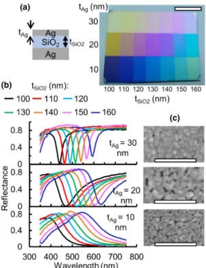
The optical cavities in Figs.1and2are based on 10 nm top Ag layer and 120–130 nm SiO2that are chosen after visualizing the color space that is attained by varying the thicknesses of the Ag and the dielectric layers. For the static cavities, 10 nm top Ag layer produces shades of blue as theSiO2 thickness varies
between 100 and 160 nm [Fig.3(a)]. For increasing Ag thick-ness, the surface colors are richer, but also fainter as the absorb-ance dip (resonabsorb-ance) sharpens [Fig.3(b)]. Top-down scanning electron microscope (SEM) images of 10 nm Ag film show nanoparticle formation [Fig.3(c)]. As a result, the optical re-sponse of the cavity with the percolating top silver film exhibits a wider and deeper resonance compared to a simple cavity con-sisting of continuous and flat layers. The measured optical response is matched by the numerical simulations when the percolating behavior of the top Ag film is accounted for.
Fig. 1. Dynamic and reversible decryption of an encrypted star pat-tern generated by raising theSiO2layer by 10 nm (theSiO2thickness
is 120 nm everywhere else) by sticking and removing a PDMS patch coated with Ag nanoparticles. The star pattern is 1 cm wide.
Fig. 2. Surface colors, cross section illustrations, and reflection spec-tra for (a) optical cavities consisting of 10 nm Ag (top) forming nano-particles, 120 and 130 nmSiO2dielectric (middle), and optically thick Ag mirror (bottom) and (b) the same structure without the top Ag layer.
Fig. 3. Static cavities with varying SiO2 and top Ag thicknesses.
(a) Photograph of the cavities. (b) Measured reflectance spectra of the cavities. The top Ag thicknesses are indicated in the figures. Scale bars: 1 cm. (c) SEM images of top Ag films.
The color space for the modular cavities is similar to that of the static ones for the top Ag thickness of 10 and 20 nm with slight shifts in the surface colors as a result of the refractive in-dex of PDMS being larger than that of air [Fig.4]. The SEM images of the silver films on PDMS exhibit similar behavior to those on SiO2 surfaces explaining the similarity of the color spaces. However, the surface colors of the static and modular cavities for 30 nm Ag thickness do not match, possibly due to the damages the silver film accumulates during repetitive sticking and removal of the patch.
The color contrast for changing dielectric thickness is more crucial than the surface color for the proposed operation. Thus, the color contrasts for 10 nm thick patterns are tested by varying the thicknesses of the top Ag film and theSiO2layer. The results show clear color contrasts for the thickness range of 10–20 nm for Ag and 120–140 nm for SiO2. Considering the observed contrasts and the robustness of the thin Ag films, the top Ag thickness is chosen as 10 nm for the following cases. While the pattern thickness for these cases is chosen as 10 nm as it is found sufficient for successful encryption and decryption, it is demonstrated that the patterns can be as thin as 2 nm to be successfully distinguished when decrypted.
The versatility of our approach is demonstrated using rigid and flexible substrates. Silicon wafers are the first choice as they are readily available in a lab environment and are suitable for any microfabrication process such photolithography [Figs.5(a)
and 5(b)]. Most of the patterns are created using stenciling (shadow masking). The stencils are produced by laser cutting of 150 μm thick acetate sheets. While this method enables large-scale images, the resolution is limited with the laser-cut-ting process and the thickness of the stencil. An alternative is photolithography that is capable of producing high-resolution, large-area patterns. Figure 5(c) shows a decrypted QR code pattern created using photolithography. The QR code is com-pletely invisible to the naked eye without the PDMS patch. The code is revealed by sticking the Ag-coated PDMS patch on and can be scanned after enhancing the contrast of the image.
As our approach involves blanket deposition of thin films and stenciling for creating patterns, it can be adapted for any substrate, including the flexible ones such as plastic sheets and aluminum foils [Figs.5(d)and5(f )]. The use of metal foils is especially promising, as they can provide both mechanical support and high reflectance acting as the bottom mirror. The use of flexible substrates helps to bring down the fabrica-tion cost and, more importantly, enables optical security fea-tures on almost any surface that can hold a metal layer such
as banknotes. Creating a multicolor pattern is also possible by defining the pattern using multiple thicknesses [Figs. 5(g)
and 5(h)]. In this case, however, most of the pattern can be detected by the naked eye without the top Ag film. Thus, it is not suitable for optical data encryption, but can only be used for authentication.
The optical data encryption relies on invisibility of the pat-terns without the PDMS patch and a noticeable color contrast with the patch on. Therefore, there is a lower limit on the pat-tern thickness to successfully decrypt the patpat-terns and an upper limit to properly encrypt them. The upper limit strongly de-pends on the reflectance of the mirror layer and can be larger for higher reflectance. For instance, a perfect mirror with 100% reflectance would demonstrate the same performance with a lossless dielectric layer of any thickness on it. Thus, the patterns can have any thickness and still be invisible to the naked eye. For an actual metal mirror, however, the reflectance is lower than 100% and with a dielectric layer on top of the mirror, absorption of the incident light further increases as a result of enhanced interaction of the light and the metal. In this case, a small change in the dielectric thickness can shift the reflection spectrum significantly enough to be noticed by the naked eye.
Fig. 4. Photograph of the modular optical cavities formed by stick-ing 10, 20, and 30 nm Ag-coated PDMS patches. Scale bars: 1 cm.
Fig. 5. Examples using various substrates and fabrication methods. (a)–(b) Hiding and revealing the pattern in a cavity on a Si substrate. The baseSiO2thickness is 120 nm. SeeVisualization 1for dynamic
decryption and re-encryption. (c) Revealed QR code pattern. The base SiO2thickness is 135 nm.Visualization 2shows dynamic decryption
and re-encryption. The use of (d) plastic and (e)–(f) Al foil as flexible substrates. Al foil is also coated with a 120 nm Ag mirror. Thus, the foil only serves as a mechanical support. (g)–(h) A flower pattern generated by changing theSiO2thickness from 90 nm (for the background) to 160 nm (for the center) by 10 nm increments in a clockwise direction. Scale bars: 1 cm.
For instance, while 10 nm thickness difference in theSiO2 di-electric layer is completely invisible on a high-reflectance Ag layer; it can be noticed by the naked eye at certain angles of view and lighting conditions for a Ag layer with lower reflec-tance. Therefore, for proper encryption, either high-reflectance metal mirrors should be used or patterns should be ultrathin at the expense of color contrast.
For the proposed function, an adhesion layer between the mirror layer and the substrate is necessary, as without it the bottom mirror peels off of the substrate while removing the PDMS patch. Just as importantly, PDMS patch should be fresh and be treated withO2plasma to increase the adhesion of the absorber layer. Without these precautions, the absorber layer is partially transferred on surfaces upon sticking and removing the patch.
The optical cavities exhibit an angle-dependent response as characterized by varying-angle spectroscopic measurements and observed by the naked eye while changing the angle of view. Although the angle-dependent response is undesired for many applications such as color printing applications [25–27], it is helpful for the proposed application, as it enables finding an angle of view that maximizes the color contrast. Furthermore, patterns changing colors with the angle of view are the basis of many optical security (authentication) tags, stickers, and strips.
The final study is testing the endurance of a modular cavity by repeatedly sticking and removing the PDMS patch. Neither the PDMS patch nor the bottom part of the cavity shows any deterioration optically or mechanically after 200 cycles. However, it is observed that dust particles are captured between the patch and theSiO2surface. The accumulation of such un-desired particles may adversely affect the optical performance during the decryption operation, especially for patterns with high resolution. This limitation can be mitigated by keeping the surfaces clean at all times. Another limitation of the method is the degradation of the top metal layer over time due to ex-posure to air. Possible solutions include using more resilient materials, e.g., Au, coating the metal layer with a thin barrier layer, and using metals that grow native oxide self-limiting the degradation process [22].
In summary, this Letter demonstrates the realization of modular optical cavities consisting of thin Ag-coated PDMS patches andSiO2-coated bottom mirrors. Patterns defined as nanometer-thick changes in the dielectric layer are encrypted without the PDMS patch and decrypted when the patch is stuck on the pattern, defining a new optical security modality. The proposed method can be employed for optical data encryp-tion, as well as security (authentication) features aiming anti-counterfeit applications.
Funding. Türkiye Bilimsel ve Teknolojik Araştirma Kurumu (117E203).
REFERENCES
1. B. Baloukas and L. Martinu, Optical Thin Films and Coatings, A. Piegari and F. Flory, eds., 2nd ed. (Woodhead Publishing, 2018), pp. 633–666.
2.“U.S. Currency Education Program,”https://www.uscurrency.gov/. 3. D. E. Denning,Am. Sci. 107, 83 (2019).
4. M. Qin, M. Sun, R. Bai, Y. Mao, X. Qian, D. Sikka, Y. Zhao, H. J. Qi, Z. Suo, and X. He,Adv. Mater. 30, 1800468 (2018).
5. G. Bakan, S. Ayas, M. Serhatlioglu, C. Elbuken, and A. Dana,Adv. Opt. Mater. 6, 1800613 (2018).
6. Q.-Y. Lin, E. Palacios, W. Zhou, Z. Li, J. A. Mason, Z. Liu, H. Lin, P.-C. Chen, V. P. Dravid, K. Aydin, and C. A. Mirkin,Nano Lett. 18, 2645 (2018).
7. X. Duan, S. Kamin, and N. Liu,Nat. Commun. 8, 14606 (2017). 8. J. Xue, Z.-K. Zhou, Z. Wei, R. Su, J. Lai, J. Li, C. Li, T. Zhang, and
X.-H. Wang,Nat. Commun. 6, 8906 (2015).
9. Q. Dai, M. Ouyang, W. Yuan, J. Li, B. Guo, S. Lan, S. Liu, Q. Zhang, G. Lu, S. Tie, H. Deng, Y. Xu, and M. Gu,Adv. Mater. 29, 1701918 (2017).
10. M. Makhsiyan, P. Bouchon, J. Jaeck, J.-L. Pelouard, and R. Haïdar,
Appl. Phys. Lett. 107, 251103 (2015).
11. D. Franklin, S. Modak, A. Vázquez-Guardado, A. Safaei, and D. Chanda,Light Sci. Appl. 7, 93 (2018).
12. B. Gallinet, F. Lütolf, L. Duempelmann, G. Basset, A. Luu-Dinh, M. Schnieper, and C. Bosshard, Photonic and Phononic Properties of Engineered Nanostructures VII(International Society for Optics and Photonics, 2017), p. 101121E.
13. H. Hu, J. Tang, H. Zhong, Z. Xi, C. Chen, and Q. Chen,Sci. Rep. 3, 1484 (2013).
14. K. Zhong, J. Li, L. Liu, S. Van Cleuvenbergen, K. Song, and K. Clays,
Adv. Mater. 30, 1707246 (2018).
15. Y. Meng, F. Liu, M. M. Umair, B. Ju, S. Zhang, and B. Tang,Adv. Opt. Mater. 6, 1701351 (2018).
16. F. Yue, C. Zhang, X. Zang, D. Wen, D. B. Gerardot, S. Zhang, and X. Chen,Light Sci. Appl. 7, 17129 (2018).
17. J. Li, S. Kamin, G. Zheng, F. Neubrech, S. Zhang, and N. Liu,Sci. Adv. 4, eaar6768 (2018).
18. S. Sun, W. Yang, C. Zhang, J. Jing, Y. Gao, X. Yu, Q. Song, and S. Xiao,ACS Nano 12, 2151 (2018).
19. M. R. Carro-Temboury, R. Arppe, T. Vosch, and T. J. Sørensen,Sci. Adv. 4, e1701384 (2018).
20. E. O. Polat, H. B. Uzlu, O. Balci, N. Kakenov, E. Kovalska, and C. Kocabas,ACS Photonics. 3, 964 (2016).
21. Z. Li, S. Butun, and K. Aydin,ACS Photonics 2, 183 (2015). 22. S. Ayas, A. E. Topal, A. Cupallari, H. Güner, G. Bakan, and A. Dana,
ACS Photonics 1, 1313 (2014).
23. J. Luan, J. J. Morrissey, Z. Wang, H. G. Derami, K.-K. Liu, S. Cao, Q. Jiang, C. Wang, E. D. Kharasch, R. R. Naik, and S. Singamaneni,
Light Sci. Appl. 7, 29 (2018).
24. L. Liang, D. B. L. Teh, N.-D. Dinh, W. Chen, Q. Chen, Y. Wu, S. Chowdhury, A. Yamanaka, T. C. Sum, C.-H. Chen, N. V. Thakor, A. H. All, and X. Liu,Nat. Commun. 10, 1391 (2019).
25. A. S. Roberts, A. Pors, O. Albrektsen, and S. I. Bozhevolnyi,Nano Lett. 14, 783 (2014).
26. M. A. Kats, R. Blanchard, P. Genevet, and F. Capasso,Nat. Mater. 12, 20 (2013).
27. G. Bakan, S. Ayas, T. Saidzoda, K. Celebi, and A. Dana,Appl. Phys. Lett. 109, 071109 (2016).