Т 4
-S -S 9 а .
MODELING AND CHARACTERIZATION OF CAPACITIVE
MICROMACHINED ULTRASONIC TRANSDUCERS
A DISSERTATION
SUBMITTED TO THE DEPARTMENT OF ELECTRICAL AND ELECTRONICS ENGINEERING
AND THE INSTITUTE OF ENGINEERING AND SCIENCES OF BILKENT UNIVERSITY
IN PARTIAL FULFILLMENT OF THE REQUIREMENTS FOR THE DEGREE OF
DOCTOR OF PHILOSOPHY
By
Ayhan Bozkurt
January 5, 2000
Ί к
l l o o a
I certify that I have read this thesis and that in my opin ion it is fully adequate, in scope and in quality, as a thesis for the degree of Doctor of Philosophy.
/··■ ///'
/ b k l l a h Atalar, Ph. D. (Supervisor)
I certify that I have read this thesis and that in my opin ion it is fully adequate, in scope and in quality, as a thesis for the degree of Doctor of Philosophy.
f
Hayrettin Köyjıen, Ph. D.I certify that I have read this thesis and that in my opin ion it is fully adequate, in scope and in quality, as a thesis for the degree of Doctor of Philosophз^
11
I certify that I have read this thesis and that in my opin ion it is fully adequate, in scope and in quality, as a thesis for the degree of Doctor of Philosophy.
I certify that I have read this thesis and that in my opin ion it is fully adequate, in scope and in quality, as a thesis for the degree of Doctor of Philosophy.
Tayfun Akin, Ph. D.
Approved for the Institute of Engineering and Sciences:
Prof. Dr. Mehmet^^;i№ay
ABSTRACT
MODELING AND CHARACTERIZATION OF CAPACITIVE
MICROMACHINED ULTRASONIC TRANSDUCERS
Ayhan Bozkurt
Ph. D. in Electrical and Electronics Engineering
Supervisor: Prof. Abdullah Atalar
January 5, 2000
The Capacitive Micromachined Ultrasonic Transducer (cMUT) is a device used for the generation and detection of ultrasonic sound waves. The device is constructed on a sil icon substrate using a microfabrication process. Individual cells constituting the device are membranes which have dimensions in the order of tens of microns, and are made up of a mechanicalh^ strong compound of silicon. The transducer itself has dimensions mea sured in centimeters, thus the total number of cells that make up a transducer is in the order of thousands. The excitation/detection of acoustic waves relies on the capacitance between the substrate and membrane: The presence of acoustic waves induces a small -AlC variation on the DC bias on the device, which can be used for detection, while a small -A.C component added to the DC bias by the drive circuit changes the electro-static attraction force on the membrane causing it to vibrate, producing acoustic waves. Basic advantages of cMUT devices include easy patterning of array structures, integration of drive/detection electronics with mechanical structures, and low cost.
In this study, basic theory describing the characteristics of cMUT devices were de veloped. The analytic formulation was used to test the validity of a Finite Element
Method (FEM) model. The FEM model, then, was emplo3'ed in the analysis of struc tures for which no analytical models are present. Specific problems solved using the FEM model included the characterization of cMUT devices with judiciously patterned electrodes. A more specific study showed that the bandwidth of an immersion device with an active area of radius 25 /¿m can be increased by 100% by simply setting the electrode radius to 10 /rm. The FEM analysis was, then, extended to handle the effects of substrate loss, which required the incorporation of an Absorbing Boundary Condition (ABC) into the model. A Normal Mode Theory analysis was conducted to give better insight to the physical nature of the effect of substrate loss to device characteristics. The dominant wavemode for a transducer of central frequency 2.5 MHz was found to be the lowest order anti-symmetric lamb wave mode (AO), for a silicon substrate of thickness 500 //m. A microfabrication process was developed for the production of cMUT devices. Hexagonally shaped transducers of radius 40 p.m were fabrictated on a conducting sili con substrated with silicon nitride as the sacrificial la.j'er and amorphous silicon as the membrane material. Both the gap and membrane thicknesses are set to 0.5 //m. 8, 16, and 24 /im gold plates were deposited as top eletrodes. The total number of active cells were 24 thousand for a substrate size of 0.7x0.7 cm^. Some experimental results were obtained from the fabricated transducers to support the analytical cMUT model. The device is found to have a central frequency of 2 MHz.
Keywords :
Capacitive Micromachined Ultrasonic Transducer (cMUT), Finite Ele ment Method (FEM) Modeling, Absorbing Boundary Condition (ABC), Normal Mode Theory, Microfabrication Process.ÖZET
KAPASİTİF MİKRO-İŞLENMİŞ ULTRASONİK ÇEVİRİCİLERİN
MODELLENMESİ VE KARAKTERİZASYONU
Ayhan Bozkurt
Elektrik ve Elektronik Mühendisliği Doktora
Tez Yöneticisi: Prof. Dr. Abdullah Atalar
5 Ocak 2000
Kapasitif Mikro-işlenmiş Ultrasonik Çevirici (kMUÇ), ultrasonik ses dalgalarının üre tilmesi ve algılanması için kullanılan bir cihazdır. Cihaz, silikon bir taban üzerinde mikro-fabrikasyon yöntemiyle üretilir. Cihazı oluşturan hücreler, boyutları on mikro nlar mertebesinde olan ve silikonun mekanik olarak sağlam bir bileşiğinden yapılan zarlardır. Çeviricinin kendisi santimetre cinsinden ölçülebilen boyutlara sahip olduğu için bir çeviriciyi oluşturan toplam hücre sayısı binlerle ifade edilir. Akustik dalgaların uyarılması/algılanması, zar ile taban arasındaki kapasitansa dayanır: Akustik dalgaların varlığı, cihaz üzerindeki DC öngeriliminde algılama için kullanılabilecek küçük bir AC dalgalanmaya j’ol açarken, sürücü devre tarafından DC öngerilime eklenen küçük bir AC bileşen zar üzerindeki elektrostatik çekim kuvvetini değiştirerek zarı titreştirip akustik dalgalar üretir. Dizilim (array) yapılarının kolay biçimlendirilmesi, mekanik yapıların sürücü/algılama devreleriyle entegras}'onu ve düşük maliyet kMUÇ cihazlarının temel a^·antajları arasında yer almaktadır.
Bu çalışmada, kMUÇ cihazlarını karakterize etmekte kullanılan temel teoriler gelişti rilmiştir. Analitik formulasyon, bir Sonlu Eleman Metodu (SE.M) modelinin doğruluğunu
sınamak için kullanımıştır. SEM modeli, daha sonra analitik modeli bulunmayan yapıların analizinde kullanılmıştır. Elektrotları belli amaçlar için biçimlendirilmiş kMUÇ’larm analizi, SEM modeli kullanılarak çözülen özel problemler arasında yer almaktadır. Daha özel bir çalışma, sualtı uygulamaları için kullanılan 25
fim
yarıçaph bir cihazın elek trot yarıçapının 10fim
yapılmasıyla cihazın bant genişliğinin % 100 arttırılabileceğini göstermiştir. SEM analizi, daha sonra taban kayıplarını da içerecek şeklide genişletilmiştir. Bu, SEM modeline Emici Sınır Koşulları’nm (ESK) eklenmesini gerektirmiştir. Ajaıca bir Normal Mod Teorisi analiziyle problemin fiziksel temelinin daha iyi anlaşılabilmesi sağlanmıştır. Bu analizle, merkez frekansı 2.5 MHz ve taban kalınlığı 500fim
olan bir çevirici için hakim dalga modunun en düşük sıralı anti-simetrik Lamb dalgası modu olduğu tespit edilmiştir. Bu çalışmada ayrıca kMUÇ cihazlarının üretimi için bir mikro- fabrikasyon yöntemi geliştirilmiştir. Bu yöntemle, zar malzemesi olarak amorf silikop, kalıp malzemesi olarak da silikon nitrat kullanılarak 40fim
çaplı altıgen biçimli çeviriciler üretilmiştir. Zar ve hava boşluğu kalınlıklarının her ikisi de 0.5fim
olarak seçilmiştir. Zarlar, elektrot olarak kullanılmak üzere 8, 16 veya 24fim
çaplı altın plakalarla kaplan mışlardır. 0.7x0.7 cm^’lik bir çevirici alanı üzerinde 24 bin aktif hücre inşaa edilmiştir. Merkez frekansı 2 MHz olarak ölçülen çeviricilerden analitik kMUÇ modelini destekleyen ölçüm sonuçları alınmıştır.Anahtar Sözcükler:
Kapasitif Mikro-işlenmiş Ultrasonik Çevirici (kMUÇ), Sonlu Eleman Metodu (SEM), Emici Sınır Koşulları (ESK), Normal Mod Teorisi, Mikro- fabrikasvon Yöntemi.ACKNOWLEDGMENTS
I would like to express my sincere gratitude to Dr. Abdullah Atalar for his supervision, guidance, suggestions and encouragement through the development of this thesis.
’I
I would like to thank to the members of my dissertation jury for reading the manuscript and commenting on the thesis.
I am indebted to Dr. Khuri-Yakub of the Ginzton Laboratory at Stanford University for providing the means for a summer internship. Many thanks are due to Dr. Degertekin and Dr. Ladabaum for their cooperation during my studies at the Ginzton Laboratory.
I would also like to thank to Dr. Ekmel Ozbay for his support during the experimental work at the Physics Department. Special thanks go to Erhan Ata, Murat Güre, and Burak Temelkuran who have been my teachers in the clean room.
Endless thanks to Sanlı! Not only an excellent colleague, he has always been my most supporting friend.
And I would like to express my sincere gratitude to the following people: Güçlü, Bacar, Tolga, Gürkan, Uğur Oğuz, Gün, Lütfİ3'e, for being my friends; Beygo, for giving life; Tünay, Hayri, Melis, for being there whenever I needed them; and Gülbin, for her endless support. Finally, like to thank to my parents, brother and Ebru, whose understanding made this study possible.
Contents
1 INTRODUCTION
1.1 Analysis 1.2 Experiment . . 31
2 ULTRASONIC TRANSDUCERS
2.1 The Micromachined Ultrasonic Transducer 2.2 Operational Principles and Parameters
3 ANALYTIC MODEL for cMUTs
3.1 Mason's Equivalent Circuit
3.2 cM UT Parameters; Collapse Voltage
3.3 cM UT Parameters: Bandwidth of Immersion cM UT
4
FEM MODELING OF cMUTs
4.1 Thermal and Electrostatic Analyses
4.2 Calculation of Electrostatic Pressure
6
6
910
10 12 1315
16 174.3 A N S Y S Modeling of cM UT 18
5
STATIC and DYNAMIC SIMULATION
20
5.1 Static A n a ly s is ... 21
5.1.1 First Order Iteration (Small D eflectio n )... 22
5.1.2 Static Analysis - Membrane Collapse V o lta g e ... 23
5.1.3 Static Analysis - Input C a p a cita n ce ... 25
5.2 Dynamic Analysis 26 5.2.1 Dynamic Analysis - Membrane Impedance 26 5.2.2 Dynamic Analysis - Electro-mechanical Transformer Ratio 26 '/
6 OPTIMUM IMMERSION cMUT
29
6.1 Partially Metalized cM UT - Membrane Sh a p e ... 316.2 Partially Metalized cM UT - Transformer Ratio 31 6.3 Partially Metalized cM U T - Simulation R e s u lt s ... 34
6.3.1 Bandwidth of cM UT - Constant B i a s ... 34
6.3.2 Bandwidth of cM U T - Variable B ia s ... 35
7 cMUT LOSS MODELING
38
7.1 FEM Model for Substrate C o u p lin g ... 397.2 Acoustic Impedance of cM UT with Loss 42
7.3 cM UT Loss vs. Model Dimensions 46
Ill
7.4 Normal Mode Theory A n a lysis... 47
8
DEVICE FABRICATION
54
8.1 An Introduction to M icrofabrication... 54 8.2 cM UT F a b rica tio n ... 55 8.3 Device D im ensions... 63 8.4 SEM Im a g e s ... 65 8.5 Experimental Setup 67 8.6 Measurement Results 708.7 Discussion and Further Work 72
9 CONCLUSION
73
A A MICROMACHINING GLOSSARY
76
B MATERIAL PARAMETERS
78
List of Figures
2.1 Schematic views of two silicon cMUT structures. 2.2 3D visualizations for various cMUT structures.
3.1 Equivalent electrical circuit for the cMUT membrane.
4.1 Metal object surrounded by medium of dielectric constant e. 4.2 ANSYS Model of Circular MUT.
4.3 Finite element mesh of the model geometry.
5.1 Application of temperature on model geometry. 5.2 Structural loads on model geometry.
5.5 Steps of iterative electrostatic-structural solution.
5.6 Iteration results for a stable and a collapsing membrane. 5.7 Acoustic impedance of membrane with zero residual stress.
11 18 19 19 21 22 22
5.3 Clamped MUT membrane model...
5.4 E-filed intensity (left) and membrane deflection (right) for V =100 Volts. 23 24 25 27
6.1 Reduced electrical circuit for the cMUT membrane... 29
6.2 Electro-mechanical transformer ratio, capacitance and bandwidth of cMUT transducer for electrode radius ranging from 2 to 24 /rm. 34 6.3 Butterworth network for electrical matching... 35
6.4 Normalized transducer bandwidth for two electrode sizes... 36
6.5 Collapse voltage values for varying electrode sizes... 36
6.6 Transducer bandwidth for DC bias equal to the collapse voltage... 37
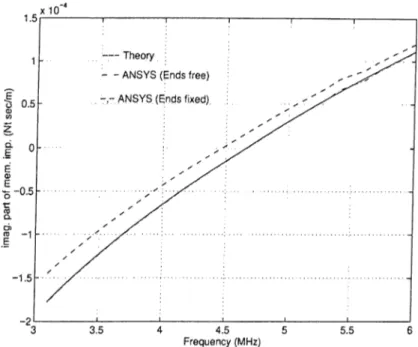
7.1 Cross-sectional view of cMUT structure. 39 7.2 Finite-element model of the cMUT... 40
7.3 Magnitude of nodal displacement on substrate (Left 1.0, Right 3.0 Mhz). 41 7.4 Fitted curve on ANSYS damp parameter determined by trial-and-error. . 42
7.5 Impedance of cMUT with substrate loss (real and imaginary parts) 42 7.6 Real impedance for a point contact... ■. . . . 43
7.7 Submodeling I : Substrate impedance. 43 7.8 Real substrate impedance for circular excitation... 44
7.9 Two-port representation for the cMUT membrane... 44
7.10 Submodeling II : Membrane as a two-port... 45
7.11 Forces at the rim of the membrane... 45
7.12 cMUT Impedance: unified and two-part m o d e l s ... 46 7.13 Real part of cMUT impedance for various substrate thicknesses. 47
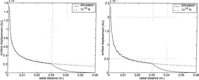
7.14 Lowest (0th) order symmetric and antisymmetric plate modes (SO and AO). 47 7.15 Dispersion curves for AO and SO modes in the frequency range 1.0-3.0 MHz 49 7.16 Particle velocity field distribution (Aq and FEA) at 1 MHz (ri=29.9 mm). 50 7.17 Total power coupled to the substrate and powers for Aq and Sq modes. 51
7.18 Equivalent circuit model which includes cMUT substrate lo.ss. 51 7.19 Total loss resistance of cMUT and resistances of
A
q andSo
modes... 52 7.20 Equivalent circuit model revisited: modal loss accounts for total loss. 538.1 Process steps 1, 2a, 2b, 2c, 2d and 3. 58
'/ 8.2 Process steps 4a, 4b, 4c, 4d, 4e and 5a... 59 8.3 Process steps 5b and 5c... 60 8.4 Top view of cMUT structure for various fabrication steps... 60 8.5 Zoomed view of mask (active membrane area 500x250 /xm^ approx.). 63 8.6 Basic building block used in drawing the cMUT mask. 64 8.7 SEM images of fabricated cMUT devices... 66
8.8 Experimental setup for cMUT characterization. 67
8.9 Detection circuit for cMUT. 68
8.10 Ginzton detection circuit for cMUT. (courtesy Dr. Sanlı Ergun) 69 8.11 Real and imaginary parts of cMUT impedance for various bias voltages. . 70 8.12 Simplified model for cMUT with ohmic losses... 71 8.13 Experimental results and model data... 71
List of Tables
4.1 Analogous field and material q u a n tities... 16
7.1 Device dimensions for the anatyses... ... 39 ■/
8.1 Equipment used in cMUT fab rication ... 55
8.2 Chemicals used in sample cleaning 56
8.3 Process charts 1-4 61
8.4 Process charts 5-8 62
8.5 cMUT fabrication process parameters. 64
8.6 Shunt input capacitance of cMUT as a function of electrode radius. 71
C hapter 1
INTRODUCTION
The generation and detection of ultrasonic waves has long been a concern in many fields of technology which include imaging, a general name for applications ranging from medical ultrasound to underwater acoustics; and nondestructive evaluation (NDE), which covers a huge set applications such as fiow measurement, material characterization, detection of holes/cracks/fractures, assessment of bonding quality of layered material, etc. In almost all applications, piezo-electric transducers were the unique choice, as alternatives such as capacitive transducers did not perform well when compared to their ultrasonic counterparts. Air-coupled and immersion capacitive ultrasonic transducers had long existed [1-3] and their characteristics and performance had been exhaustively evaluated. However, until recent developments in micromachining techniques which have led to the design of new versions of the devices [4-10], those were not considered as serious alternatives for piezo-electric transducers.
Piezo-electric transducers exploit a physical phenomenon called “piezoelectricity”: an electric field causes a crystal structure to change its shape, or reversely, a crystal produces an E-filed when it’s shape is changed. Capacitive ultrasonic transducers, on the other hand, use electrostatic forces: changing the charge on the plates of a capacitor
changes the mutual attraction force, causing the plates to displace. Likewise, a change in the plate displacement, when the voltage is held constant, causes a current to flow either out from, or in to the capacitor. A capacitive Micromachined Ultrasonic Transducer, is a collection of thousands of small capacitors with one plate being in the form of a free-to-vibrate membrane, each cell having dimensions in the order of tens of microns.
Capacitive Micromachined Ultrasonic Transducers (cMUT), have the same qualities of the piezo-electric transducers, when power output, dynamic range and operation fre quency are concerned. However, there are three basic advantages associated with cMUTs which deserve mentioning; First, they perform better in air. Materials used in the fab rication of piezo-electric transducers usually have acoustic impedances in the order of 30x10® kg/m^s, 5 orders of magnitude higher than that of air (400 kg/m^s). There has been a great effort in the development of matching layers, but these did not produce sat isfactory results as either materials with desired acoustic impedances were not available, or the matching layer was required to be impractically thin, or the matched transducer turned out to have a a very narrow band. However, proper adjustment of design pa rameters for cMUTs result in transducers that perform quite well even at frequencies as high as 11.4 MHz [6]. A second advantage is about the convenience in fabrication of complicated structures, such as array transducers. Piezo-electric array transducer pro duction requires the use of fine mechanical processing tools, and employs a cumbersome wiring step to connect the transducer to drive/detection electronics. For cMUTs, how ever, structures are pattered using standard lithography, which makes the fabrication of fancy structures quite convenient, and the drive electronics can be even constructed on the same substrate, removing the necessity for wiring. Third, silicon processing is a widely available well-established method. Therefore, cMUT devices are fabricated very cheapljc
Theories explaining the electro-mechanical properties of piezo-electric transducers have been well established, and the behavior of fabricated transducers can be precisely
predicted. Unfortunately, the same does not apply to cMUTs. Some theory and analysis methods explaining their operation have been proposed [4,7,11-13]. Still, the behavior of these devices require comprehensive analysis and design parameters must be well eval uated. As main motivational forces behind transducer development include applications in air-coupled NDE, new structures for efficient ultrasonic transmission into air need to be developed. Likewise, designs for 3-D immersion imaging using 2-D transducer ma trices require a good understanding of coupling between array elements. Furthermore, for all applications, sources of mechanical loss need to be evaluated, as the spectral characteristics of the device are greatly affected by loss.
This study has two focus points: the development of analysis tools for the evaluation of cMUT characteristics, and the experimental verification of proposed analysis meth ods. For the first objective, a lumped circuit representation for the cMUT device was developed by the help of numerical analysis tools. For the second, a microfabrication process was developed and implemented in a clean room environment. We now discuss both parts of the thesis in more detail:
1.1 Analysis
The basic analysis method to evaluate the performance of micromachined structures is to use an electrical equivalent circuit and express evaluation criteria in electrical terms such as insertion loss, or electrical bandwidth. Mason proposed an lumped electrical equivalent circuit for capacitive transducers [14]. This model has been extensively used in our analj'^ses to verify numerical results. Chapter 3 describes Mason’s model in detail.
Mason’s model describing cMUT characteristics only applies to particular device structure. Real-life structures, however, usually do not satisfy conditions to make the Mason’s model valid. As there are no closed form expression describing the behavior of those devices, numerical methods need to be employed. Chapter 4 describes how the
cMUT device is modeled using the Finite Element Model (FEM) and how eletrostatic and mechanical FEM probems can be coupled.
The FEM model proposed in Chapter 4 is first used to regenerate the results of Mason, and was found to produce correct results, as described in Chapter 5. Simulation for real-life structures are run and results are assessed bj^ comparing them to heuristic expectations. Simulations are then extended to accuratel}'^ work out device parameters (e.g., the collapse voltage) which are just estimated by Mason’s model.
One parameter of significance is the bandwidth of the transducer which, basically, determines the pulse response of the device. Part of this study focuses on the bandwidth optimization of immersion transducers, using anatysis, tools developed in Chapter 5. Although electrode patterning has been used for selective mode excitation of resonators, [15] and in the optimization of capacitive pressure transducers and microphones [16], there is no comprehensive study in the literature on the performance optimization of capacitive micromachined ultrasonic transducers (cMUTs) using electrode patterning. In Chapter 6 we present optimization criteria, analyses, and simulations which demonstrate that electrode patterning can be used to significantly enhance the performance of cMUTs.
Power coupled to anywhere other than the loading medium is considered as a loss term for a transducer.The basic loss mechanism for capacitive micromachined ultrasonic transducers is the power coupled to the substrate. Surface wave modes on solid half spaces and acoustic waveguides have been extensively studied [17]. The power coupled to these nodes can be determined by matching the stress amplitude at the membrane rirn to the wave amplitudes of these nodes. Consequently, loss can be incorporated into the lumped model of the cMUT. The same analysis can be used to determine cross-coupling to neighboring transducer elements. The amount of loss and cross-coupling is significant in the determination of transducer bandwidth and array performance. Chapter 7 finds out values for loss terms to be incorporated in Mason’s model. A modal theory analysis is included to give better insight to the physical nature of coupling to surface wave modes.
1.2 Experiment
Chapter 8 discusses a microfabrication process developed for the production of ch-IUT devices. There are well established fabrication processes reported in literature [4 ,6 ,1 8 - 20]. Here, we mimic the Stanford fabrication process described in [20], but we use our own mask design and process sequencing, and make use of equipment available in the Advanced Research Laboratory of the Physics Department of Bilkent University. The fabricated devices are found to have reasonable electrical performance, despite their low reliability. Although the experiments do not provide full support to the anal3Tic results, they still provide good insight to the fabrication techniques, and their electrical characteristics are well explained by a very basic model which is the starting point of the entire modeling work.
'I
All of the analyses described in Chapters 5 and 6 assume a transducer of circular shape, as an FEM model for a circular structure is easily generated. However, the fabricated transducers are of hexagonal shape to allow close packing. This will have an insignificant effect on device characteristics, and the analysis for a circular transducer will apply to the hexagonal structure.
To summarize, research work described in this thesis includes:
• Electrical Modeling of Capacitive Micromachined Ultrasonic transducers • Optimization of device characteristics using electrode patterning.
• Modeling of mechanical losses using both FEM anal}^sis results and mode theory. • Development of a microfabrication process for the production of cMUT devices.
C hapter 2
ULTRASONIC TRANSDUCERS
Ultrasonic transducers are devices capable of converting electrical signals into ultrasound and vice versa. They find wide application in the fields of non-destructive evaluation and medical imaging. Advances in microfabrication techniques enabled the construction of micromachined versions of these devices with significant advantages described in this chapter.
2.1 The Micromachined Ultrasonic Transducer
The almost universally used transducer type is that constructed using piezoelectric ma terials [17]. Though being very commonly used, piezoelectric transducers have low con version efficiency and their operation is limited to relatively low frequencies, because of mechanical limitations on the production of small devices. For improved system per formance and high resolution imaging, efficient high frequency transducers are required. Capacitive Micromachined Ultrasonic Transducers (cMUTs), perform much better than their piezoelectric counterparts in terms of the mentioned figures of merit. Microma chined ultrasonic tran.sducers [8,11,12,21], are produced using standard silicon processes
and are distinguished with their efficiency, strength and reliability.
Fig. 2.1 shows the cross-sectional view of two different cMUT devices. The device in the upper schematic has a vibrating membrane consisting of silicon nitride, supported by a silicon oxide layer. A thin gold layer is plated to act as an electrode. The silicon
i .J y w J .
Silicon;·.,
^ T o p Electrode ^Silicon Nitride
. Í M x ,iw iw ir> v t i> <t»Ílíí5wMéííV;*^
Figure 2.1: Schematic views of two silicon cMUT structures.
substrate on which the device is constructed is the second electrode. The device’s me chanical action is due to the electrostatic attraction force between the two electrodes. The device is circular, the dashed line in the figure showing its axis of rotation. The cen tral cavity into which the membrane can deflect is vacuumed. The vibrating membrane of the device in the lower schematic is supported by the silicon nitride layer itself.
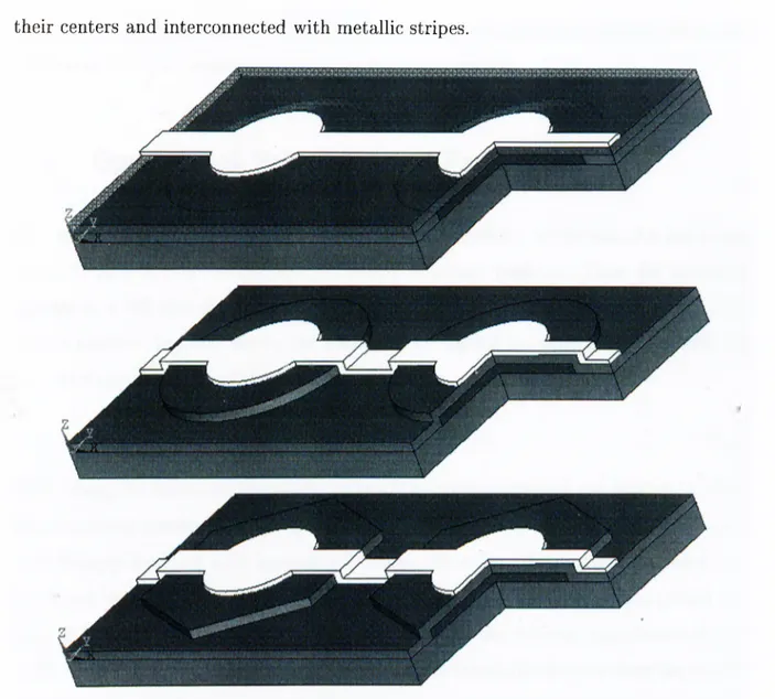
Fig. 2.2 shows 3-D visualizations for various cMUT structures. The top figure corre sponds to the upper drawing in Fig. 2.1: the membrane layer is supported by the sac rificial layer from which cylindrical openings are cut. The upper layer is made slightly transparent to show the gap. For the structures shown in the central and lower drawings, the membrane is formed by shaping the membrane layer itself: at certain regions the membrane material is raised to form a gap. This gap can be either circular, as in the cen tral drawing, or hexagonal (lower figure), latter of which results in more closely packed membranes. All drawings show two membranes with circular top electrodes placed at
their centers and interconnected with metallic stripes.
Figure 2.2: 3D visualizations for various cMUT structures.
The production technique involved in the fabrication of the latter structure will be described in Chapter 8.
One obvious advantage of capacitive transducers constructed using a rnicromachining process is that the accompanying electronics can be constructed on the same substrate on which the device resides. This results in noise immunity (as the cabling between the transducer and driving/receiving electronics is eliminated) and ease of production (e.g., no flat parallel cables are required to be connected to array elements). Many foundries
now offer mixed micromachining/electronics processes for which the micromachining part is done as a step of the standard device production process.
2.2 Operational Principles and Parameters
As mentioned, the cM UT’s activation is due to electrostatic attraction. An important point to note is that electrostatic attraction is always positive. Thus, for harmonic operation, a DC bias should be applied to make sure that the voltage on the cMUT is always positive. In other words, the voltage to be applied in between the top electrode and substrate should be of the form
V{t) - V
d c+ VAcsin{uit)
(
2.
1)
with
u
being the excitation frequency. As it will be further analyzed, the applied DC bias is an important parameter which determines the device’s efficiency. The effect is positive, i.e., efficiency increases with increasing DC bias. Therefore, the maximum allowed DC bias which does not causes the membrane to collapse down to the substrate (which we will callVcoiiapse)
is of importance. On the other hand, the inherent capacitance of the device is another design consideration. Patterning the top electrode can reduce the device capacitance, but this reduces the device efficiencjc However, capacitance and efficiency have complex dependencies on electrode shape. Thus, an optimum point for device performance can be found by judiciously patterning the top electrode. Simulation results showing the validity of the last argument will be presented in the following chapters.C hapter 3
ANALYTIC MODEL for cMUTs
In this chapter, we describe the model used in the anal3^sis of capacitive micromachined" ultrasonic transducers (cMUT) and present some theoretically derived parameters of the device. The theoretical derivations are verified by simulations which will be described in subsequent chapters.
3.1
Mason's Equivalent Circuit
The anah'sis of the cMUT structure is based on the equivalent circuit approach of Ma son [14] as adapted in [4]. The model, as seen in Fig.3.1, consists of a shunt input capacitance Co at the electrical port and an electro-mechanical transformer with turns ratio 1 : n. is the lumped acoustic impedance of the membrane and
Z[
is the acoustic load, which is just the acoustic impedance of the mediumZmedium.
multiplied by the membrane areaSmembrane- V
andi
show the input voltage and current, respective!}'. F is the total electrostatic force on the membrane under the assumption that electrostatic pressure is uniform at all points. For the lumped model, the measure for the membrane movement is its average velocityv.
11
+ o ^ AV
o
-f o O - - - 'Electrical Port
A coustic Port
Figure 3.1; Equivalent electrical circuit for the cMUT membrane.
According to Mason [14], the membrane deflection is described bj'· the diff'erential equation
(r„ +
T )t
d'^x
(3.1) where is the membrane thickness,
T
is the residual stress in the membrane material,Y
q is the Young’s modulus,S
is the Poisson’s ration,p
is density andP
is the applied pressure. For harmonic excitation, we have(Yo
+T ) t
nV y - t n T
- P - o j t n p x = 0
12(1 - ¿2)where w is the frequency. Boundary conditions for a clamped diaphragm are
ddy
(3.2)
y(^) |r=0 — 0)
ddr
= 0. (3.3)Solving eqn. 3.2 with the above boundary conditions we get
y{r)
= (^2û)^o(^P’) "bk\J\{ki(i)Ii){k2T)
^^ptn _k2Jo{k\(i)Ji(k2Q·)
+k\J\{k-[(x)lQ{k2(i)
with where ,\/d'^ +
4co;2 —d
,\/^~+4cuP + d
ki = \ l
--- ^ --- ;k2
= V — 2c ^ A{Yo + T )tl
2c
(3.4) (3.6) (3.6) 12(1 - <S2) ’-This solution assumes that pressure
P
has constant amplitude for all r. The equation fory{r)
will be used to justify simulation results. The average velocityv{u)
of the membrane12
IS
ra
v{üj) = juj27r
/ ry{r) dr.
Jo
(3.7)Substituting the above expression for
y(r),
the membrane impedanceZa = {'Ka?)P/v{w)
is found as3<^ptn
Za =
'Ka^
f e # 4+
A:i74H l 2 { k ' i - k k l )k\ k 2 d 7 J o ( k i a ) 1 7 I o { k 2 a ) r ' ^ J x i k i a ) k\k2CL 1 2 { k \ + k l ) (3.8)This expression for
Za
will be used to check the membrane impedance found b}^ simula tions. Furthermore, equationZa
yields an analytic expression for the resonance frequency of the cMUT membrane.3.2 cM UT Parameters: Collapse Voltage
When the DC bias voltage applied to the membrane exceeds a critical value, the mem brane collapses over the silicon membrane. This critical voltage
{VcoUa.pse)
be found by modeling the membrane as a parallel plate capacitor suspended above a fixed ground plate with a linear spring. The spring constant(
k)
can be found as the ratio of pressure to volume displacement; [14]T A ta
K — where c = (3,9) 12p(l — a^) ’^
p
(3.10)with T,
p
anda
being the residual stress, density and Poisson’s ratio of the membrane material, andA
being the area of the membrane. Ifx
denotes the membrane displace ment, the total restoring string force is13
The electrostatic force on the membrane is given by
Ae^V^
F,
(3.12)2co
{tn -\r
x)'j
The voltage to keep the membrane at a certain deflection
x
can be found by equating toFs
and solving forV.
The critical voltage at which the membrane becomes unstable can be determined by finding the displacement for whichdV jdx —
0. Solving yieldsa; = ^ (¿a +
and the corresponding collapse voltage is found as
(3.13)
Kcollapse
1
8
k(ta
+2TÁ7a
(3.14)3.3 cM UT Parameters: Bandwidth of Immersion cM UT
If the cMUT transducer is assumed to be a parallel plate capacitor, its capacitance ise
A
Ca =
For small deflections of the membrane,
(tn +
(3.15)
E{r,t) = V it)/itn + - Q
^0 (3.16)
Thus,
T{r, t)
= ^ —(U^c(^) + 2 1 ...VDc{r)VAcir) SixiLOt)/{tn
, . . .s +—ta)^
e (3.17)2 €o ' . . .
and the electro-mechanical transformer ratio n (which is the time varying part of T(r,t) times the membrane area divided by the AC voltage) is
,2
. T/ ^
14
Consequents^ the RC time constant r of the transducer (which is given as r =
CoZil-n?)
isr = £ s J _
v i a \
in -i---- in ) to^l-
(3.19) Eq. 3.14 contains the spring constant k of the membrane as a term, which is has an approximate expression [14]^ _ 16 7T
Y
qtl
(1
- ’Substituting this into the collapse voltage expression of Eq. 3.14, we get
(3.20)
collapse
12S Y o tl (i„ + J i „ ) ’
(3,21) 2 7 e o (l-i) 2 )tt· '
Combining Equations 3.19 and 3.21 }delds the expression for the time constant
_ 2 7 0 ^ / ) ^
^ 128 Eo
tl
where Zu, is the acoustic impedance of the loading medium. This equation shows that the bandwidth of the cMUT does not depend on the air gap thickness when
V
dc is at(3.22)
collapse-The resonance frequency
fc
of the cMUT membrane is [14] (2.4)2I
f c =
tn (3.23)2
tt Y 12p(l —6^) a~
If a cMUT is to operate at a certain frequenc.y,
tn/a^
has to be constant when adjusting device dimensions to increase bandwidth. This condition, when combined with Eq. 3.22 implies that the device bandwidth linearly increases with increasing membrane thicknessC hapter 4
FEM MODELING OF cMUTs
Usually, complex mechanical structures cannot be analyzed using analytic models. In·/ those cases, the Finite Element Method (FEM) can be employed to obtain numerical solutions to problems. Theoretical derivations for the behavior of clamped circular mem branes [14] allow the evaluation of a single type of transducer geometry. For different geometries and boundary conditions simulations are run using ANSYS Rev.5 .2 [22-25].
The FEM software package ANSYS is unable to handle static electrical problems. However, many commercially available FEM packages (including ANSYS) are able to solve field problems of the Laplace and Poisson type, which include heat conduction problems. Although, not usually stated in software references, these programs are able to solve electrostatic field problems, as well. The analogy between the governing differential equations of these two types of problems enables a direct substitution of corresponding field and material quantities [26].
We first present the theoretical tools employed in the simulations and then explain how the cMUT was modelled using ANSYS.
16
4.1 Thermal and Electrostatic Analyses
In heat conduction, Poisson’s equation describes a problem in which the temperature distribution r is to be solved from a known heat generation g in a medium of known heat conduction /c, which turns out to be
v ^ r =
-(ilk
(4.1)for an isotropic medium. The electrostatic counterpart of this equation, the field quantity to be determined is the scalar potential
(j)
given the charge distribution p in a region of permittivity e, which, in turn, isV V = - p / e (4.2)
again for an isotropic medium. An immediate observation of Eqns. 4.1 and 4.2, and
■
,
further noting that the scalar potential is related to the electric field intensityE
byE
= suggest the following table for analogous field and material quantities (viz. table 4.1). The only consideration when making substitutions for the listed field andThermal Electrical
k
(conductivity) r (temperature)q
(heat generation) V r (temperature gradient)e
(permittivity)(p
(scalar potential)p
(charge density)—E
(electric field intensity) Table 4.1; Analogous field and material quantitiesmaterial quantities is that corresponding quantities for the thermal and electrical prob lems should be in the same system of units. The solution data should be interpreted accordingly, as well.
17
4.2 Calculation of Electrostatic Pressure
The total force acting on a volume charge distribution
p
due to an external electric field E is given byF = y
Y^dV
(4.3)where F„ is the volume density of force, defined as
Ft, =
pE
(4.4)The force expression given in Eqn. 4.3 is a function of both field and charge. According to the Faraday-Maxwell field theory, force can be expressed as a function of the field only, as force is transmitted by means of the field. This suggests the existence of a force
•I
function T on the surface enclosing the volume in consideration such that
f F y d V = [ T d S
Jv
Js
(4.5)where T is called the Maxwell Stress Tensor. After some vector manipulation, the expression for T is found as
T = eo
(n ■
E)E -
(4.6)where n is the surface normal. For a rigorous derivation, the reader is advised to refer to [27], pp.112-113. Consider now that we have a metallic object of arbitrar}'^ shape, placed in a non-conducting medium with electric permittivity
e.
We would like to find an expression for T , noting that this problem requires additional treatment as Fqn. 4.6 is for a non-dielectric medium. Before proceeding, we observe that E is perpendicular to the object surface (i.e., E = E n), so that n · E = E. Hence, if the metal object were in vacuum, the expression for T would beE 2
r = (4.7)
However, the object is surrounded by a medium of permittivity e. Consider that we have an infinitesimally thin layer of vacuum between the object surface and the enclosing
18
Ô-^O
. '_^d·
Figure 4.1; Metal object surrounded medium of dielectric constant e.
medium, as depicted in Fig. 4.1. From the Gauss’ flux theorem, E =
(e/eo)Ed,
where E and Ed are electric field vectors in vacuum and dielectric, respectively. Combining this with Eqn. 4.7 results in^2
p2
T = - ^ n (4.8)
which is the desired stress expression for the metal object in dielectric.
4.3 A N SYS Modeling of cMUT
ANSYS supports the modeling of T h erm a l and S tru ctu ra l elements. One ANSYS element type of this category is SOLID13 which can be used individually as an element having thermal or structural degrees of freedom, or it can be employed in an anal}'^sis where the effects of both are coupled. Throughout the work presented, the former anal ysis type is used as the thermal model is employed just to work out the solution of the electrical problem, and thermo-structural effects, such as thermal expansion, have noth ing to do with the problem in hand. Hence, the structural and thermal (i.e., electrical) problems are handled separately and their coupling is provided by “artificial” means, which will be the discussed in the following sections.
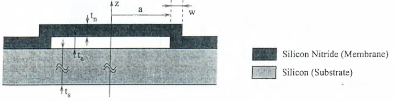
The MUT whose static and dynamic electro-mechanical properties are to be investi gated is modeled as a two dimensional axisymmetric solid. Elements of this type basically define a volume of rotation around the y-axis. Thus, rectangles with one edge aligned with the y-axis model cylinders, and the view on the computer screen turns out to be a
19
side view of a slice cut out of the particular cylindrical object to be modeled. Fig. 4.2 depicts the two dimensional model for the silicon MUT to be analyzed. All regions are
\ y (Roimional Syinmciiy Axis)
---
28pin---
25|jm-l.Ojum 'S.Opin· Silicon Nitride | B I Silicon Oxide [, ■ j Air
Figure 4.2: ANSYS Model of Circular MUT.
bound to each other at boundaries. The air layer is modeled using a solid element, too. It is there just to provide a coupling medium for the electrical FEM analysis, and as it has low stiffness, low density, it does not perturb the structural solution. The actual membrane has a very thin gold layer on top of the Si3Ni4 layer as an electrode, whose effect can be safely ignored for the structural analysis. Therefore it is not included in the FEM. Likewise, the whole structure lies on a silicon substrate, which will be modeled by defining structural boundary conditions. Electrical potential will be input to the model by defining nodal temperatures at the top and bottom lines (planes).
The next step in the FEM analysis of the cMUT is meshing. Fig. 4.3 shows a coarse
i m n i EEEEEB KBiiBi!;
Figure 4.3: Finite element mesh of the model geometry.
version of the mesh used in simulations. As the element type used in simulations has both degrees of freedom, thermal and structural solutions are obtained using the same mesh. The number of mesh divisions are adjusted to have reasonable accuracy.
C hapter 5
STATIC and DYNAMIC SIMULATION
The static (DC) and dj^namic (harmonic) simulations of the cMUT are done separatel}'^ as ANSYS does not support a combined structural analysis. The static analysis of the cMUT membrane 3uelds
- The shape and capacitance of the device for an applied DC bias, - The collapse voltage (KoHapse),
- E-filed values to be used in the djmamic analysis.
The dynamic analysis, using results of the DC solution, provides - The mechanical impedance of the membrane,
- The electro-mechanical conversion efficiency (transformer ratio).
Results of both analyses are then used to determine “component values” of the equivalent circuit. In the following sections we present simulation results together w'ith analytic figures to show the accuracy of the FEM model.
21
5.1 Static Analysis
The static displacement of the membrane is of interest in the determination of the shunt input capacitance, the collapse voltage and field quantities for the harmonic analysis. All of these require the determination of the membrane shape for an applied DC voltage. The static analysis of the membrane deflection is done by first solving the electrostatic problem, then computing the resulting pressure and finally performing a structural anal ysis to find the effect of electrostatic forces on the structure. It is apparent that once structural deformation occurs, the electrostatic solution is altered, which is the source of the deformation. Therefore, the problem is non-linear in nature which calls for an iterative solution. Once the structural deformation is found, the electrostatic problem should be solved once again, followed by another structural analysis, and so on. In each analysis step, the Thermal package of ANSYS is used to find the electrostatic field " for a certain metalization size. Fig. 5.1 shows the application of thermal loads to the undeflected model geometry. E-field intensity at the electrode-membrane boundary is
h y y Nodes @ 1 °C ^ Nodes @ 0°C V V V V V V V V V V V V V y y V V V V V V V V V V 5 7 0 . . ■ '
'
' A,g.·S
f:llii
'Aqni;
'»V-'vm
w
1
;X
·
i
a" '"A >1S
i
'h' ‘3
F
ii
3
^
2
, "iA3
immmrrmmnm
n
nmrm
m i l l
Figure 5.1: Application of temperature on model geometry.
found by computing the thermal gradient. Then, we employ the Maxwell Stress Tensor equation (5 .1 ) to find the electrostatic pre.ssure on the membrane:
T o c ir) = n — E lc{r).
¿Co
(5.1)The computed pressure values are, then, applied as structural loads to the model geom etry as depicted in Fig. 5.2.
22
i\y ► Movement Constraint (y -a x is )
À Movement Constraint (x -a x is )
III Pressure on Element Face
iiiiiiiiiiiiiiiiiiiiiiiiiiiiiiiiiiiiiiiiiiiiiiiiiii III III III III Uj,
I
Figure 5 .2 : Structural loads on model geometry.
5.1.1
First Order Iteration (Small Deflection)
The accuracy of first order simulation results is tested by comparing the simulated de flection data with results of analyses from theory [14]. Mason, in his model, assumes that the membrane’s end is clamped and the applied pressure is uniform on the membrane surface. The ANSYS model for the MUT has no clamping at the membrane ends. To test the validity of out model, modifications depicted in fig. 5.3 has been made. Here,
AY ► Movement Constraint ( y -a x is )
k Movement Constraint (x -a x is )
III Pressure on Element Face
- IWIW Wl Wl IW W W III Wl W W WIWWIW W WUW m HI tii
·» s
m0,
^r£
%Ç&
ÎK m m m % w : : mv> .-i··
M
^
^SUf ^
Figure 5.3: Clamped MUT membrane model.
the membrane is clamped right at the start of the support and all pressure components are set to have a constant ,value. Hence, simulation conditions are set as close as to the assumptions of the derived equations.
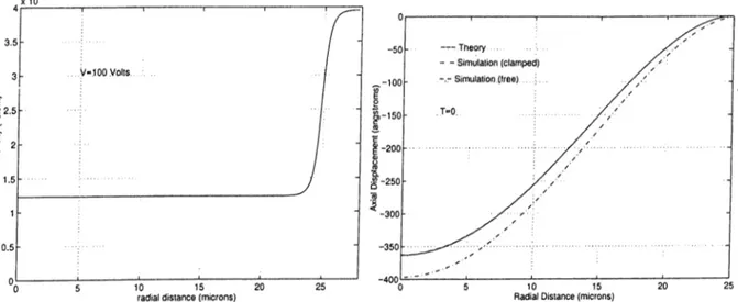
The results are striking. Fig. 5.4 shows the analytic membrane deflection together with two simulation results; one for a clamped membrane and the other for a free one, the latter being a better result when judged by closeness to reality. The simulation result
23
for the clamped membrane shows that the model produces results in excellent agreement with theory, as it can be seen from the plot, and a closer look at numerical data shows that results are correct within the third decimal digit. The simulation for the “real” membrane deflects slightly more than theory’s prediction. This is basically due to the boundary condition. The Silicon Oxide support, although being very stiff, can still be compressed, 5delding non-zero values for deflection and its derivative at the membrane boundary. Moreover, electric field intensity gets higher at the upper electrode - Silicon Nitride boundary as going away from the center of the membrane towards the supported part of it (see fig. 5.4).
Figure 5 .4 ; E-filed intensity (left) and membrane deflection (right) for V =100 Volts.
5.1.2 Static Analysis - Membrane Collapse Voltage
As mentioned at the very beginning of the section on static analysis, structural changes aflPect the electrostatic problem and, hence, an iterative solution is required to determine the membrane shape for larger deflections. The problem is not very involved. Once the deflection is determined, the electrostatic problem is re-solved. The new set of elemental pressure values is then used to find a new structural solution. The iteration continues
24
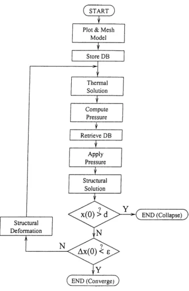
until either an infinitesimal change occurs in shape or the membrane collapses. Fig. 5.5 shows a fiow-chart describing the iteration, where
e
is the stopping criteria,d
is the height of the.air gap and y(r) is the membrane deflection at a radial distance r. TheFigure 5.5: Steps of iterative electrostatic-structural solution.
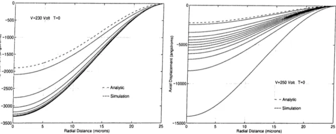
iteration to determine the membrane shape is terminated either when the membrane shape stabilizes or when the membrane collapses onto the substrate. For the former case the applied voltage is lower than the collapse voltage, while for the latter case the applied voltage is above the collapse voltage. The collapse voltage is the value of the DC bias at which the membrane is infinitesimally close to collapse. Figure 5.6 shows iteration results for a stable and collapsing membrane, respectively. The applied voltages are 230
25
Figure 5.6: Iteration results for a stable and a collapsing membrane.
and 250 Volts. The collapse voltage for this particular membrane is some value between these voltages. The trace labeled “Analytic” is the result of the analytical treatment assuming uniform deflections and forces.
5.1.3 Static Analysis - Input Capacitance
The results of the static analysis are used to determine the shunt input capacitance C'o(Vdc)^ of the transducer. For a certain DC bias voltage, the shape of the membrane is determined by the iterative simulation described above. Once the electric field intensity at the deflected membrane surface is known, the charge distribution on the electrode is found using Gauss’ Theorem. The capacitance of the membrane for various electrode sizes is determined by computing the total charge on the membrane and dividing this by the applied voltage. So, if
E ocir)
is the electric field intensit}',Со(Уос)
is given by27Гб
'DC
6f
2 тгбC
o(V
dc)
=7 ^ f E
dc ·ds
= — /r Eocir)
VDC Js
V
dcJ
odr.
{5.2}
Voc-26
5.2
Dynamic Analysis
The aim of the dynamic (harmonic) analysis is the determination of additional model parameters of the equivalent electrical circuit: the lumped acoustic impedance of the membrane Z«, and the electro-mechanical transformer ratio n.
5.2.1 Dynamic Analysis - Membrane Impedance
The acoustic impedance
Za
of the membrane is found by first findingv(u))
for zero acoustic load (i.e., the cMUT in vacuum) and a uniform excitation pressure at the set of frequencies of interest, and then dividing the total force on the membrane by these■/
velocity values. The accuracy of the analysis is tested by comparing the simulated impedance values to analytical results. Mason [14], in his formulation of the membrane’s mechanical behavior, assumes that the membrane ends are clamped. The same boundary conditions are imposed during simulations for test purposes. For the stated boundary conditions, there is a remarkable match between the analytical and numerical results. The actual membrane’s ends are not clamped; rather, they rest on the sacrificial oxide layer. Simulation results for this case show that the resonance frequency of the actual membrane is slightly less than that of the clamped membrane. Fig. 5.7 shows the two simulation results together with the analytic impedance curve.
5.2.2 Dynamic Analysis - Electro-mechanical Transformer Ratio
As previously stated,electrostatic forces generated by a voltage are always attractive, regardless of the polarity of the applied voltage. Hence, a voltage of the form
27
Figure 5.7: Acoustic impedance of membrane with zero residual stress.
with
V
dc >V
ac is applied to the membrane to assure harmonic motion. The applied DC biasV
dc will cause the membrane to deflect towards the substrate. We assume thatV
ac results in a small harmonic motion compared to the DC deflection and also assume that the cMUT membrane behaves like an ideal plate capacitor so that uniform E-field exist on the membrane surface. The, the resulting electric field intensity ist)
—E
dc +E
ac sinU)t
(5.4) withr
being the radial distance from the membrane’s center,Er,c{‘>')
the E-field intensity at the membrane-electrode boundary for the DC bias, and17 _
V
ac jp^AC —
77—^DC-F,D C
(5.5) The electrostatic pressure on the membrane can be found using the Maxwell Stress Tensor equation
T(i) = n
6o 2 (5.6)
where n is the surface normal of the metal electrode and
e
is the relative permittivity of the membrane material. Substituting Eq. 5.4 into Eq. 5.6 and ignoring second order28
terms gives the temporal and spacial variation of electrostatic pressure on the cMUT surface:
f V2
=
^TT'^DC
+ n —£ ’£,c-£^.4CSinwi The total AC forceF
ac oii the membrane isF
aC
= (tTU) —E
dcE
aC
=A — F
dcV
aC { tn
d---ta
€q ^0 V Co
and consequently the electro-mechanical transformer ratio is
6^
f
e ^ ^ =F
acI'^AC —
-A —VDcf tnd----¿a Co V eo - 2 (5.7) (5.8) (5.9)The electro-mechanical transformer ratio, n, determines by how much the effect of the mechanical properties of the membrane are reflected to the electrical port, as shown in' Fig. 3.1.
Chapter 6
OPTIMUM IMMERSION cMUT
When the cMUT is used as an immersion device (i.e., loaded with a relatively high acoustic impedance liquid such as water) the acoustic impedance of the cMUT membrane
Za
and the loadZi
form a low quality factor circuit. In such cases, the membrane impedance can be neglected for frequencies near the mechanical resonance of the device. The equivalent circuit, then, reduces to a simpler network containing Z/, Co and the electro-mechanical transformer. Fig. 6.1 shows the reduced model for the cMUT used asZ/ =
t
VCo
- o ---- ___ I
Electrical Port Acoustic Port Equivalent Circuit Figure 6.1: Reduced electrical circuit for the cMUT membrane.an immersion device. Here, we limit our discussion to the effect of the shunt capacitance Co on the efficiency and bandwidth of the device. If bandwidth were not a concern, one could simply tune out Co with an inductor to achieve zero insertion loss. But bandwidth is indeed a concern, ,so a more complete formulation of the optimization objective is to