a thesis submitted to
the graduate school of engineering and science
of bilkent university
in partial fulfillment of the requirements for
the degree of
master of science
in
material science and nanotechnology
By
˙Irfan Selim Bozdo˘gan
January 2019
CATION EXCHANGE METHOD
COLLOIDAL SYNTHESIS OF Ag(I)-DOPED
CdSe NANOPLATELETS WITH PARTIAL
COLLOIDAL SYNTHESIS OF Ag(I)-DOPED CdSe
NANOPLATELETS WITH PARTIAL CATION EXCHANGE
METHOD
By ˙Irfan Selim Bozdo˘gan January 2019
We certify that we have read this thesis and that in our opinion it is fully adequate, in scope and in quality, as a thesis for the degree of Master of Science.
Hilmi Volkan Demir(Advisor)
D¨on¨u¸s Tuncel
Evren Mutlug¨un
Approved for the Graduate School of Engineering and Science:
Ezhan Kara¸san
Director of the Graduate School ii
iii
ABSTRACT
COLLOIDAL SYNTHESIS OF Ag(I)-DOPED CdSe
NANOPLATELETS WITH PARTIAL CATION
EXCHANGE METHOD
İrfan Selim BozdoğanM.S. in Material Science and Nanotechnology
Advisor: Hilmi Volkan Demir
January 2019
Colloidal nanoplatelets (NPLs) exhibit strong one-dimensional quantum confinement in the vertical direction. This makes them a highly attractive host system for studying variable doping techniques and effects without variation in the quantum confinement effect. Earlier, core-only CdSe NPLs were converted into Cu2Se and HgSe NPLs, and also CdSe/CdS core/shell NPLs were transformed into Cu2Se/Cu2S, ZnSe/ZnS, and PbSe/PbS NPLs by using full cation exchange (CE) methods. Recently, core-only CdSe NPLs have been doped with Cu(I) ions using high-temperature nucleation doping and post-synthesis partial CE approaches. On the other hand, unlike Cu(I), such monovalent doping with Ag(I) ions has previously not been possible in NPLs as a host system, although silver doping had been widely studied in other host systems. Therefore, there has been no previous report on the doping of Ag(I) into CdSe NPLs to date. To address this gap, in this thesis, Ag(I) doping in CdSe NPLs by using a post-synthesis partial CE technique was developed. A systematic study was carried out to investigate the effects of dopant precursor reactivities, reaction timing, and temperature on the evolution of dopant-related emission as compared to the excitonic emission. In controlled experiments, the excitonic emission peak was eliminated and only dopant-related emission peak was successfully obtained. Finally, temperature-dependent emission kinetics of the as-synthesized Ag(I)-doped CdSe NPLs at varied temperatures ranging from 25 to 298 K were investigated. It was observed that both excitonic and dopant-related emission peaks were blue-shifted and their intensities were considerably increased with the decreasing temperature. As a new dopant-host
iv
system, these Ag(I)-doped CdSe NPLs hold a great promise for further systematic spectroscopic studies and possibly various optoelectronic applications.
Keywords: Semiconductor nanocrystals, colloidal nanoplatelets, doping, partial cation
v
ÖZET
GÜMÜŞ-KATKILI CdSe NANOLEVHALARIN KISMİ
KATYON DEĞİŞİMİ METODU İLE KOLLOİDAL
SENTEZİ
İrfan Selim BozdoğanMalzeme Bilimi ve Nanoteknoloji, Yüksek Lisans Tez Danışmanı: Hilmi Volkan Demir
Ocak 2019
Kolloidal nanolevhalar dikey yönde kuvvetli tek boyutlu quantum sınırlaması gösterirler. Atomik olarak düz bu nanolevhaların dikey yöndeki sınırlaması, kuantum sınırlama etkisinde değişiklik yapmadan, değişik katkılama tekniklerini ve etkilerini incelemek için, bu nanolevhaları oldukça çekici bir mesken sistem yapmaktadır. Tam katyon değişimi (KD) metotları kullanılarak, CdSe çekirdek nanolevhalar Cu2Se ve HgSe nanolevhalara; CdSe/CdS çekirdek/kabuk nanolevhalar ise, Cu2Se/Cu2S, ZnSe/ZnS, and PbSe/PbS nanolevhalara dönüştürülmüştür. Yakın zamanda, CdSe çekirdek nanolevhalar yüksek sıcaklıkta çekirdekleşme ve kısmi KD yaklaşımları ile Cu(I) ile katkılanmıştır. Öte yandan, Cu(I)’in aksine, gümüşün diğer mesken sistemlerde genişçe çalışılmasına rağmen, nanolevhaların mesken bir sistem olarak daha önce tek değerli gümüş iyonları ile katkılandırılması mümkün olmamıştır. Bu yüzden bu güne kadar daha önce hiçbir çalışmada CdSe nanolevhaların gümüş katkılamasının izine rastlanmamaktadır. Bu ihtiyacı gidermek için, bu tezde, ilk defa, Ag(I) nin kısmi katyon değişimi metodu kullanılarak, CdSe nanolevhalarına katkılanması metodu geliştirilmiştir. Öncü katkılayıcıların reaktiviteleri, reaksiyon süreleri ve sıcaklığın etkileri için katkılayıcı-bağlantılı ışımanın gelişimi eksitonik ışımaya kıyaslanması sistematik çalışmalar yapılarak araştırılmıştır. Kontrollü deneyler ile eksitonik ışıma tepesi ortadan kaldırımış ve katkılayıcı-bağlantılı ışıma tepesi başarıyla elde edilmiştir. Son olarak, Ag(I)-katkılı CdSe nanolevhalarının 25-298 K aralığındaki sıcaklığa bağlı ışıma kinetiği incelenmiştir. Gözlemlenenlere göre düşük sıcaklıkta hem eksitonik hem de katkılayıcı-bağlantılı tepeler maviye kaymış ve şiddetleri gözle görülür şekilde artmıştır. Yeni katkılayıcı-mesken bir sistem olarak
vi
Ag(I)-katkılı CdSe nanolevhalar ileri sistematik spektroscopik çalışmalara ve çeşitli optoelektronik uygulamalar için çok gelecek vaadeden malzemelerdir.
Anahtar sözcükler: Yarıiletken nanokristaller, kolloidal nanolevhalar, katkılama,
vii
Acknowledgement
I must first express my gratitude to my supervisor Prof. Hilmi Volkan Demir, who gave me the opportunity to study in nanoscience, supported my research and gave me numerous valuable suggestions in my project and writing up this thesis.
I also want to thank Assoc. Prof. Dönüş Tuncel and Assoc. Prof. Evren Mutlugün for serving on my thesis committee.
The entire Demir Research Group has made my two years of research enjoyable. Every past and present members of this group are appreciated. In such a friendly group, I received not only lots of help but also enjoyed my research. In particular, I want to thank Dr. Murat Olutaş, Dr. Manoj Sharma, Dr. Savaş Delikanlı, and Dr. Yusuf Keleştemur, who always shared their knowledge and lab skills with me. I wish to thank all members of UNAM where I do not have space to name individually.
I would like to thank Nima Taghipour, Didem Dede, Esma Uçar, Beria Keser, Ibrahim Tanriöver, Furkan Işık, Mustafa Sak, Safa Şengezer, Muhammet Furkan Özkan and Ömer Kürşat Turan for their friendship and the time we have had together.
I thank very much my family for their love, encouragement, support and taking an interest in my work. Finally, I thank my girlfriend, Berrak Soykarafakılı, for her endless love and help as an editor, being my escape from the stress and to overcome many challenges of life and listening to every minor laboratory success with interest.
viii
Contents
1 Introduction ... 1
1.1 Organization of the Thesis ... 3
2 Scientific Background ... 4
2.1 Colloidal Semiconductor Nanocrystals ... 4
2.2 Colloidal Synthesis ... 6
2.3 Colloidal Nanoplatelets ... 7
3 Characterization Techniques of Colloidal Nanoplatelets ... 12
3.1 Optical Characterization Techniques ... 12
3.1.1 Absorption Spectroscopy ... 12
3.1.2 Photoluminescence Spectroscopy (PL) ... 14
3.1.3 Photoluminescence Excitation Spectroscopy (PLE) ... 15
3.1.4 Time-Resolved Fluorescence Spectroscopy (TRF)... 16
3.2 Structural Characterisation Techniques ... 17
3.2.1 Transmission Electron Microscopy (TEM) ... 18
ix
4 Colloidal Synthesis and Characterisation of Silver-Doped CdSe
Nanoplatelets ... 21
4.1 Motivation... 21
4.2 Experimental ... 22
4.2.1 Chemicals ... 22
4.2.2 Preparation of Cadmium Myristate ... 23
4.2.3 Synthesis of 4 ML CdSe Nanoplatelets... 23
4.2.4 Synthesis of Ag(I)-Doped CdSe Nanoplatelets ... 24
4.3 Results and Discussion ... 24
5 Conclusion ... 52
x
List of Figures
Figure 2.1: Band diagrams of bulk and colloidal semiconductors nanocrystals.
Reprinted from Ref. [40]. ... 5
Figure 2.2: Quantum dot and their absorption and fluorescence peaks. Reprinted from
Ref. [41]. ... 6
Figure 2.3: Nucleation and growth model for colloidal nanocrystals. Reprinted with
permission from Ref. [45]. ... 7
Figure 2.4: Schematic representation of 4 ML CdSe nanoplatelets where red spheres
can be Zn or Cd and grey spheres can be S, Se or Te. ... 8
Figure 2.5: (a) Absorption and (b) PL spectra of 4 ML CdSe nanoplatelets. ... 9
Figure 2.6: Absorption and PL spectra of CdSe nanoplatelets having various
thicknesses. Reprinted with permission from Ref. [40]. ... 10
Figure 3.1: Absorption spectrum of 4 ML CdSe nanoplatelets, e-hh is electron heavy hole and e-lh is electron light hole ... 13
Figure 3.2: PL spectrum of 4 ML CdSe nanoplatelets. ... 14
xi
Figure 3.4: Time-resolved fluorescence decay curves core-only and Ag(I)-doped CdSe
nanoplatelets at 515 nm. ... 16
Figure 3.5: Basic representation of a transmission electron microscope. ... 17
Figure 3.6: A TEM image of 4 ML CdSe nanoplatelets. ... 18
Figure 3.7: A survey XPS spectrum of Ag(I)-doped CdSe nanoplatelets. ... 19
Figure 4.1: (a) Absorption and PL spectra and (b) TEM image of 4 ML undoped CdSe nanoplatelets at room temperature. ... 25
Figure 4.2: (a) Absorption and (b) PL spectra of Ag(I)-doped 4 ML CdSe nanoplatelets obtained by using 100 µL of AgNO3, 2 mL of CdSe, 15µL of TOP, 2 min reaction time and stirring time for 3 h... 27
Figure 4.3: TRF decay curves at room temperature for undoped and Ag(I)-doped 4 ML CdSe nanoplatelets obtained by using 100 µL of AgNO3, 2 mL of CdSe, 15 µL of TOP, 2 min reaction time. ... 28
Figure 4.4: (a) Absorption and (b) PL spectra of Ag(I)-doped CdSe nanoplatelets obtained by using Synthesis A. ... 29
Figure 4.5: (a) Absorption and (b) PL spectra of Ag(I)-doped CdSe nanoplatelets obtained by using Synthesis B. ... 30
Figure 4.6: Variations of heavy-hole and light-hole absorbance values with stirring time for Synthesis B. ... 31
Figure 4.7: Variations of band-edge and dopant related emission intensities with stirring time for Synthesis B. ... 32
Figure 4.8: Photoluminescence intensity versus absorbance obtained from Synthesis B for dopant emission. ... 34
xii
Figure 4.9: 𝐼0⁄ versus 𝑡 for Synthesis B. ... 35 𝐼 Figure 4.10: 𝐴0⁄ versus 𝑡 for synthesis B. ... 36 𝐴 Figure 4.11: (a) Absorption and (b) PL spectra of Ag(I)-doped CdSe nanoplatelets
obtained by using Synthesis C. ... 38
Figure 4.12: Variations of heavy-hole and light-hole absorbances with stirring time for
Synthesis C. ... 39
Figure 4.13: Variations of band-edge and dopant related emission intensities with
stirring time for Synthesis C. ... 40
Figure 4.14: (a) Absorption and (b) PL spectra of Ag(I)-doped CdSe nanoplatelets
obtained by using Synthesis D. ... 41
Figure 4.15: Variations of heavy-hole and light-hole absorbances with stirring time for
Synthesis D. ... 42
Figure 4.16: Variations of band-edge and dopant related emission intensities with
stirring time for Synthesis D. ... 43
Figure 4.17: (a) Absorption and (b) PL spectra of Ag(I)-doped CdSe nanoplatelets
obtained by using Synthesis E. ... 44
Figure 4.18: Variations of heavy-hole and light-hole absorbances with stirring time for
Synthesis E. ... 45
Figure 4.19: Variation of dopant related emission intensities with stirring time for
xiii
Figure 4.20: XPS spectra of Ag(I)-doped CdSe nanoplatelets. Survey spectrum (a),
high-resolution XPS spectra of cadmium 3d, selenium 3d and silver 4s orbitals (b-d).
... 47
Figure 4.21: PL emission spectra of Ag(I)-doped CdSe nanoplatelets including both
the dopant-related and band-edge emissions at different temperatures. ... 48
Figure 4.22: Change in the PL intensity for dopant-related emission as a function of
the temperature. ... 49
Figure 4.23: Change in the PL intensity for band-edge emission as a function of the
xiv
List of Tables
Table I: Experimental Conditions of Ag (I) -Doped CdSe Nanoplatelets from Synthesis A to E. ... 26
1
Chapter 1
Introduction
Use of transition metal ions as dopants in semiconductor colloidal quantum dots has attracted a great deal of interest for various applications [1-9]. Such doped colloidal quantum dots exhibit novel optical and electronic properties. To study and explore these properties and their optoelectronic applications, new synthesis methods for doping in colloidal quantum dots have been investigated [8, 10-14]. Various methods e.g. doping based on pre-doped precursors, nucleation doping, growth doping, ion exchange and diffusion have been reported for the synthesis of these doped colloidal quantum dots from molecular precursors [8, 15-19]. In all of these methods, nucleation, growth and surface chemistry should be controlled carefully for obtaining the required optical and electronic properties [20, 21].
Among the doping methods, cation-exchange is a simple method for the synthesis of new colloidal nanomaterials [22, 23]. In this method, undoped nanocrystals are pre-synthesized and then the doping is performed by using post-synthesis cation-exchange [22-25]. This method separates doping and nucleation process of nanoclusters which leads to controlled doping in pre-determined sized/shaped nanocrystals. In this approach, complete or partial cation-exchange can be possible. Recently, for the electronic doping of colloidal quantum dots, the partial cation-exchange has been used as a secondary method [4, 26]. In the partial cation-exchange, less number of cations
2
are exchanged by the cations in the host nanocrystals lattice. This process enables to impart novel electronic, magnetic and optical features to the starting colloidal quantum dots.
The doping of different amounts Ag (I) ions into CdSe colloidal quantum dots by controlled cation-exchange and the doping of Ag (I) and Cu (II) ions into CdSe colloidal quantum dots by using the partial cation-exchange reactions have previously been reported. They studied electronic doping effects in a very low doping regime. Therefore, these studies by partial cation-exchange methods do not show dominant and Stokes-shifted emission which is widely reported for doping in nanocrystals by high temperature methods [4, 26].
Colloidal nanoplatelets (or also known as colloidal quantum wells) have gained a great deal of attraction because of strong 1D confinement in the vertical direction [27, 28]. Giant oscillator strengths, linear and non-linear absorption cross-sections, inhomogeneous broadening suppression and spectra of narrow spontaneous emission can be mentioned in superior optical properties for nanoplatelets [29-32]. In recent years, CdSe nanoplatelets have been exchanged to Cu2-xSe and HgSe nanoplatelets by using complete cation-exchange methods [33, 34]. Generally, in 0D nanocrystals, understanding of doping effects are compromised by particle size distribution [35, 36]. Here, narrow emission line-widths due to strong vertical confinement in colloidal quantum wells and their non-size distribution effect enables them to be an important form of nanocrystals which can offer the investigation of doping effects under strong quantum confinement regimes. Recently, the Cu(I) doping in CdSe nanoplatelets by using a high-temperature nucleation doping [37] and the post-synthesis partial cation-exchange methods [35] have been carried out in our research group. Here, partial cation-exchange method helps to understand the doping mechanism and their efficient dopant related emissions, whereas the high temperature method provides near unity efficient dopant induced emission which was successfully utilized in luminescent solar concentrator applications. Like, Cu(I), Ag(I) doping in 0D nanocrystals by high temperature method shows dominant Stokes-shifted emission. Furthermore, they are shown to possess tuneable electrical property ((n-type vs p-type) depending upon the nature of doping (interstitial vs substitutional). However, in order to separate particle size distribution effects from doping effects (optical, electrical) and understand Ag(I) doping under strong quantum confinement, Ag(I) doping in nanoplatelets is needed.
3
To date, there has been no report on the doping of Ag(I) into such CdSe nanoplatelets by using the partial cation-exchange method. To address this need, in this thesis, Ag(I)-doped CdSe nanoplatelets by using a post-synthesis partial cation-exchange method is proposed and developed. A comprehensive study is carried out to find out the Ag doping into the nanoplatelets using of varying amounts of Ag(I) ions. To measure and characterize these nanomaterials, several techniques such as steady-state absorption spectroscopy, steady-state photoluminescence (PL) spectroscopy, X-ray photoelectron spectroscopy (XPS), time-resolved fluorescence (TRF) spectroscopy and transmission electron microscopy (TEM) has been used to show Ag(I) doping into these CdSe nanoplatelets and understand the mechanism and origin of their dopant related PL emission.
1.1 Organization of the Thesis
The organization of the remaining of this thesis is shown as follows.
In Chapter 2, the main themes of colloidal semiconductor nanocrystals and the colloidal nanoplatelets and their excitonic and optical properties are presented.
In Chapter 3, characterizations of the synthesized colloidal nanoplatelets by different optical and structural techniques.
In Chapter 4, the synthesis of Ag(I) doped CdSe nanoplatelets using partial cation-exchange method and their optical and structural studies are presented. The effects of different experimental factors on the synthesis and their optical properties has been elaborated. In addition, temperature-dependent PL properties of doped nanoplatelets are also studied.
4
Chapter 2
Scientific Background
In this chapter, basic concepts of colloidal semiconductor nanocrystals with the colloidal synthesis are presented. As a quasi-2D family of nanocrystals, the colloidal nanoplatelets are also discussed and their excitonic and optical properties are compared to those of the other semiconductor nanocrystals.
2.1. Colloidal Semiconductor Nanocrystals
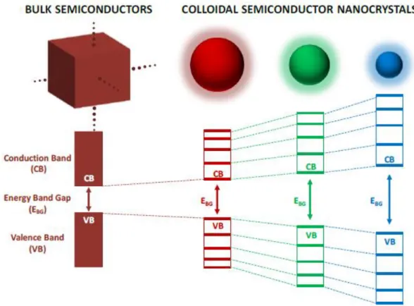
Colloidal semiconductor nanocrystals are small crystalline particles with typical dimensions ranging from 2 to 20 nm [38, 39]. Bulk semiconductors are characterized by their band gap energy. In bulk semiconductors, conduction and valence bands have continuous energy levels. However, semiconductor nanocrystals have discrete energy levels in their band structures because of their quantum confinement energy discretization, as illustrated in Figure 2.1 [40].If a photon with energy greater than the band gap of a semiconductor is absorbed by this semiconductor, the electron leaves an orbital hole in the valence band. The negatively charged electron and positively charged hole form a pair through Coulomb attraction, which is known as an exciton. Relaxation of the excited electron from the conduction band to the valence band annihilates the exciton and may result in the emission of a photon. This process is known as radiative recombination. The size of
5
exciton is defined by exciton Bohr diameter and depends intrinsically on the material. If the size of a semiconductor nanocrystals is smaller than the size of the exciton, the charge carriers are spatially confined. This raises their energy. This effect is known as quantum confinement [40].
Figure 2.1: Band gap diagrams of bulk and colloidal semiconductor nanocrystals. Reprinted from Ref. [40].
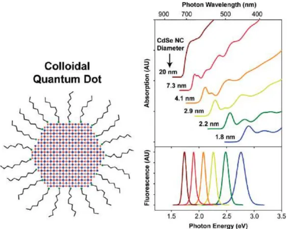
If the dimensions of nanocrystals are smaller than exciton Bohr diameter, they demonstrate size-dependent absorption and fluorescence spectra with discrete electronic transition (see Figure 2.2). Because of their discrete energy levels, semiconductor nanocrystals show narrower emission linewidth, wider spectral tunability, and faster fluorescence lifetime.
6
Figure 2.2: Quantum dot and their absorption and fluorescence peaks. Reprinted from Ref. [41].
2.2. Colloidal Synthesis
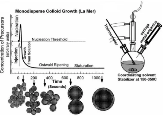
Three main constituents required for colloidal synthesis of semiconductor nanocrystals are ligands, solvents and precursors [42-44]. For the nucleation and growth, molecular precursors are broken down to monomers. Ligands are the organic molecules that are used to obtain uniform, monodisperse and stable nanocrystals. Solvents dissolve the molecular precursors and provide the colloidal stability of nanocrystals. For the colloidal synthesis of nanocrystals, the nucleation and growth model are developed by La Mer and Dinegar [45]. According to this model, steps of nucleation and growth should be separated to obtain monodispersed colloidal nanocrystals as shown in Figure 2.3. To synthesize, firstly, molecular precursor is injected into the hot reaction solution. This precursor is then decomposed, and a supersaturated solution is obtained.
7
Figure 2.3: Nucleation and growth model for colloidal nanocrystals. Reprinted with permission from Ref. [45].
First, smaller size nanocrystals provide the faster rate that is compared to the larger size nanocrystals at the beginning of the growth stage. Then, depletion of monomers is occurred at the end of the growth stage. Due to the higher surface energy, smaller size nanocrystals are dissolved, and bigger size nanocrystals are grown. Therefore, increasing of size distribution is observed. All the above process is Ostwald ripening. When the Ostwald ripening can be controlled during a synthesis, monodisperse colloidal semiconductor nanocrystals are obtained. Furthermore, the temperature and the growth time decide the size of the inorganic core. For this reason, longer growth time and higher temperatures result in larger particles [40].
2.3. Colloidal Nanoplatelets
Atomically flat colloidal nanoplatelets were first synthesized by Ithurria and Dubertret [27]. These colloidal nanoplatelets are similar to the quantum wells, thus also called colloidal quantum wells. These colloidal nanoplatelets have atomic-scale
8
vertical thicknesses and lateral dimensions with tens of nanometres. The vertical thicknesses and lateral dimensions of nanoplatelets can be controlled by changing the injection temperature and growth time. Figure 2.4 shows the schematic of a 4 monolayer (ML) thick CdSe nanoplatelets. Colloidal CdSe nanoplatelets have zinc blende crystal structure. These nanoplatelets were synthesized by slightly changing the method of CdSe colloidal quantum dots [40].
Figure 2.4: Schematic representation of 4 ML CdSe nanoplatelets where red spheres can be Zn or Cd and grey spheres can be S, Se or Te.
The lateral dimensions of nanoplatelets are greater than the exciton Bohr diameter. Therefore, nanoplatelets show strong quantum confinement typically only in their vertical thicknesses. These nanoplatelets have quasi-2D structure and possess distinct electronic and optical properties, which do not present similarity with colloidal quantum dots [28]. Because of their quantum-well like electronic structure, their absorption spectra exhibit a table-top profile below the band-edge with excitonic transitions related the transitions of heavy-hole and light hole.
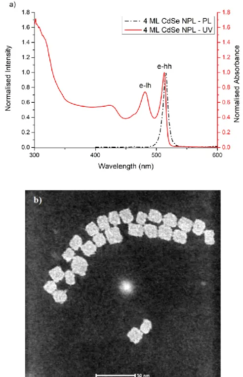
Figure 2.5 shows the absorption and PL spectra of 4 ML thick CdSe nanoplatelets. The transitions from the conduction band to the heavy and light-holes are observed at ~512 and ~482 nm, respectively. These nanoplatelets exhibit almost zero Stokes-shift along with narrow full-width-at-half maximum (FWHM) of about 10 nm in their emission spectrum. This narrow emission linewidth indicates the absence of inhomogeneous broadening [46]. Because of their strong quantum confinement effects, these atomically flat nanoplatelets have ultrafast radiative lifetimes as well as large linear and nonlinear absorption cross-sections [29, 30].
9
Figure 2.5: (a) Absorption and (b) PL spectra of 4 ML CdSe nanoplatelets.
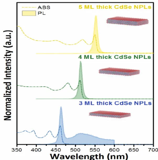
These nanoplatelets have strong quantum confinement in the vertical direction. Therefore, these colloidal nanoplatelets have discrete absorption and photoluminescence spectral properties almost independent of lateral dimensions. If the vertical thickness of the nanoplatelets is increased, the quantum confinement is relaxed and excitonic features of the nanoplatelets are shifted to the lower energies. Figure 2.6
10
shows a set of absorption and PL spectra of CdSe nanoplatelets having various thicknesses.
Figure 2.6: Absorption and PL spectra of CdSe nanoplatelets having various thicknesses. Reprinted with permission from Ref. [40].
Previously, CdSe nanoplatelets have been exchanged to Cu2-xSe and HgSe nanoplatelets by using a complete cation-exchange method [33, 34]. CdSe@CdS core@shell nanoplatelets were also exchanged to Cu2Se@Cu2S, ZnSe@ZnS and PbSe@PbS [25]. 3-5 ML of CdSe nanoplatelets were doped with Cu(I) ions by using high-temperature nucleation and partial cation-exchange methods [37]. Cu(I)-doped 1D confined CdSe nanoplatelets enables optical features such as the large Stokes-shifts
11
and absorption cross-sections, the tuneable PL emissions, and high QY. These Cu(I)-doped nanoplatelets have been shown to make excellent luminescent solar concentrators.
12
Chapter 3
Characterization Techniques of
Colloidal Nanoplatelets
The structural and optical characterization techniques are presented in this chapter.
3.1. Optical Characterization Techniques
To understand and measure the steady-state excitonic properties of the synthesized colloidal nanoplatelets, absorption, photoluminescence, photoluminescence excitation and time-resolved fluorescence spectroscopy techniques were used in this study.
3.1.1.
Absorption Spectroscopy
The absorption behaviour of nanoplatelets was measured by using the steady-state absorption spectroscopy technique. In these measurements, the synthesized samples of nanoplatelets were used for measuring the absorption spectra in the ultra-violet to visible range. These measurements were conducted with a Carry 100 model UV-Vis. Spectrometer. All samples in dispersion form were used for measuring the absorption
13
spectra in the absorbance mode configuration of the instrument. Absorbance is given by Beer-Lambert Law:
𝐴 = 𝜖𝑙𝐶 (3.1) where 𝐴 is the absorbance (unitless), 𝜖 is the molar extinction coefficient (L/mol cm), 𝑙 is the width of the cuvette (cm), and 𝐶 is the concentration (mol/L).
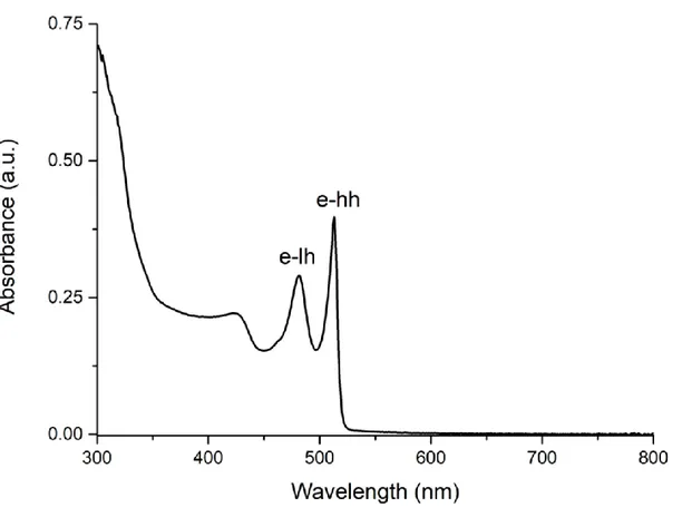
Figure 3.1: Absorption spectrum of 4 ML CdSe nanoplatelets, e-hh is electron heavy hole and e-lh is electron light hole.
Figure 3.1 represents the absorption spectrum of 4 ML core-only CdSe nanoplatelets. Excitonic transitions from the valence band to the conduction band of the CdSe semiconductor are seen in this spectrum. Conduction and valence bands are formed by Cd 5s and Se 4p orbitals, respectively. The p-orbitals are degenerated. Therefore, there are heavy hole, light hole and split-off bands in the valence band. In the absorption spectrum, the first (~512 nm) and second (~480 nm) excitonic peaks correspond to the electron-heavy hole and the electron-light hole transitions, and the third peak is called split-off band. The peak positions of these excitonic bands depend on the vertical thickness of the nanoplatelets due to their quantum confinement effect and do not
14
depend on the lateral dimensions when larger that exciton Bohr diameter. If the thickness of the nanoplatelets increases, the spectrum red-shifts. As a result, the vertical thicknesses of the nanoplatelets can be estimated by absorption spectroscopy [28, 40].
3.1.2.
Photoluminescence Spectroscopy (PL)
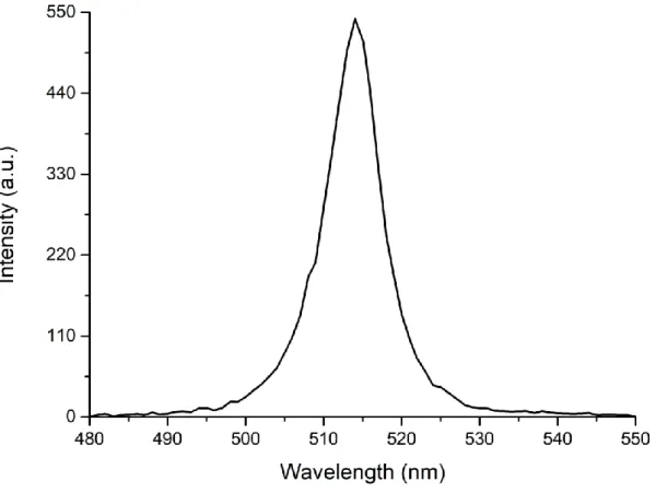
In the PL emission measurements, nanoplatelets samples in the dispersion form are excited by a fixed excitation wavelength. As a result, electron-hole pairs are formed. When these electrons recombine radiatively, the process results in photoluminescence. For the PL measurements in this thesis, Cary Eclipse model fluorescence spectrometer was used. Figure 3.2 shows the PL spectra of 4 ML CdSe nanoplatelets which exhibits a sharp emission peak centred at 515 nm with narrow emission linewidth (~10 nm). Such atomically flat nanoplatelets suppress the inhomogeneous broadening and gives the narrow emission linewidth.
15
Moreover, core-only nanoplatelets lead to discrete emission peaks (e.g. 465 nm, 515 nm, 554 nm for 3, 4, 5 ML CdSe nanoplatelets respectively). This feature enables the estimation of the vertical thicknesses of the nanoplatelets from the emission spectra [40, 47].
3.1.3.
Photoluminescence Excitation
Spectroscopy (PLE)
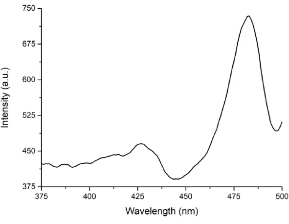
The photoluminescence excitation spectroscopy (PLE) is used together with the steady-state absorption and PL emission measurements to understand the origin of PL from the solution samples of nanoplatelets [40]. Therefore, PLE spectra of the colloidal nanoplatelets should be similar to their absorption spectra. Figure 3.3 shows the PLE spectrum of 4 ML thick CdSe nanoplatelets.
16
3.1.4.
Time-Resolved Fluorescence
Spectroscopy (TRF)
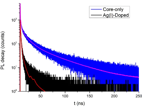
TRF is a useful technique for studying the emission kinetics of atomically flat nanoplatelets. For the TRF measurements in this thesis, Fluo-Time 300 time-resolved spectrometer together with PicoHarp 200 time-correlated single photon counting unit was used. Here, samples are excited by a pulsed laser at a specific wavelength (375 nm). The resulting decay curves are fitted by using multi-exponential function and χ2 parameter. Thus, the recombination rates in the nanoplatelets are analysed by using the fluorescence decay curves [40].
TRF decay curves of CdSe and Ag(I)-doped CdSe nanoplatelets are given in Figure 3.4. The CdSe core-only nanoplatelets show an amplitude-averaged lifetime of 0.68 ns and Ag(I)-doped CdSe nanoplatelets become slightly shorter and shows an amplitude-averaged lifetime of 0.31 ns at 515 nm.
Figure 3.4: Time-resolved fluorescence decay curves core-only and Ag(I)-doped CdSe nanoplatelets at 515 nm.
17
3.2. Structural Characterization Techniques
The dependency of optical features of the colloidal nanoplatelets are related with their structural properties. Therefore, in this master thesis, to examine the size, shape, structure and chemical composition of the synthesized colloidal nanoplatelets, transmission electron microscopy and X-Ray photoelectron spectroscopy techniques are used.3.2.1.
Transmission Electron Microscopy
(TEM)
In order to determine the size, shape, structure and composition of the colloidal nanoplatelets, transmission electron microscopy (TEM) is used as a strong imaging method.
18
In this thesis, the purpose of using TEM was to investigate the structural properties of the synthesized colloidal CdSe nanoplatelets. Figure 3.5 shows schematic representation of a typical transmission electron microscope. For the preparation of sample for TEM, the diluted solutions of colloidal nanoplatelets were cleaned few times to get rid of the excess ligands. Then, typically 5 µL of this solution was dropped onto a carbon coated copper mesh grid. In order to evaporate the solvent, the copper grid was kept under the vacuum atmosphere before any measurements were taken [40]. The nanoplatelets studied in this thesis have atomic-scale vertical thicknesses (1 - 2 nm) that in TEM imaging, the nanoplatelets demonstrate low contrast. Therefore, the imaging of these thin nanoplatelets shows a typical has been performed under scanning transmission electron microscopy mode (S-TEM). Figure 3.6 shows the typical STEM micrograph of 4ML CdSe nanoplatelets.
19
3.2.2. X-Ray Photoelectron Spectroscopy
(XPS)
To analyse the surface properties and elemental composition of colloidal nanoplatelets, XPS is used [48]. In this thesis, the XPS measurements were done by preparing a solid film samples on silicon substrates. Briefly, two-three times cleaned nanoplatelet samples in dispersion form were dropped onto a silicon substrate and were allowed to dry under vacuum. In XPS measurements, the monochromatic X-rays are irradiated onto samples and photoelectrons are collected. The kinetic energy of the emitted electrons is given by the relation:
𝐾𝐸 = ℎ𝜐 − 𝐸𝑏− 𝜙 (3.2)
where 𝐾𝐸 is the kinetic energy of the emitted electrons, ℎ𝜐 is the energy of X-rays, 𝐸𝑏 is the binding energy of the photoelectrons, and 𝜙 is the spectrometer work function [40].
Figure 3.7: A survey XPS spectrum of Ag(I)-doped CdSe nanoplatelets.
20
The intensity of the emitted electrons was recorded as a function of the binding energies. The elemental composition of our samples was analysed by using the XPS spectra. The elemental compositions of the synthesized undoped CdSe and Ag(I)-doped CdSe nanoplatelets were verified by XPS. Figure 3.7 shows a high-resolution survey XPS spectrum of Ag(I)-doped CdSe nanoplatelets.
21
Chapter 4
Colloidal Synthesis and
Characterization of
Silver-Doped CdSe Nanoplatelets
4.1. Motivation
Semiconductor colloidal nanoplatelets exhibit thickness-dependent optical properties [27, 28] because of their magic-sized vertical thicknesses and strong quantum confinement in the vertical direction. In addition to the core only nanoplatelets [49-52], different heterostructures of nanoplatelets, including core-crown [53], core@shell [54, 55], and core/crown@shell [56] have been synthesized [27, 28, 56]. Furthermore, CdSe nanoplatelets have been exchanged into Cu2Se and HgSe nanoplatelets [33, 34], and CdSe@CdS core@shell nanoplatelets have been converted into Cu2Se@Cu2S, ZnSe@ZnS, and PbSe@PbS nanoplatelets [25] by using full cation-exchange methods. Thus, in the recent years these full cation-exchange reactions have emerged as a beneficial method to get new nanostructures which are otherwise difficult to synthesize using conventional chemical methods. In addition, the optical, electrical, and magnetic
22
characteristics of nanocrystals can be altered using partial cation-exchange methods. By varying the dopant reactivities, the host cations can be replaced with dopant cations in the crystal lattice [35]. Recently, our research group has successfully synthesized Cu(I)-doped 3-4 ML thick CdSe nanoplatelets which can be obtained using high temperature [37] that Cu(I)-doped nanoplatelets were having large Stokes-shifted dopant emission with high QY were used in luminescent solar concentrators. However, the high-temperature nucleation doping method has a limited control on the doping. Doping of the different amounts Ag (I) ions into CdSe colloidal quantum dots by controlled cation-exchange [4] and doping of Ag (I) and Cu (II) ions into CdSe quantum dots by using the partial cation-exchange reactions [26] were previously reported. However, efficient dopant-related emission peaks were not found in these studies. Very recently, our research group has also shown Cu(I) doping in CdSe nanoplatelets of different thicknesses (3-5 ML) using a post-synthesis partial cation-exchange method [35]. To make Cu(I) doping via partial cation-cation-exchange, large control over doping amounts were observed. This in turn helped to understand the emergence of dopant induced emission in detail. To the best of our knowledge; there has been no report on the doping of Ag(I) into CdSe nanoplatelets by using partial cation-exchange method. To address this need, in this thesis, Ag(I)-doping in CdSe nanoplatelets by using a post-synthesis partial cation-exchange method is proposed and developed.
4.2. Experimental
4.2.1.
Chemicals
Cadmium nitrate tetrahydrate (Cd(NO3)2.4H2O) (99.99% trace metal basis), cadmium acetate anhydrous (Cd(Ac)2) (99.99%), cadmium acetate monohydrate (Cd(Ac)2.H2O) (99.99%), cadmium acetate dihydrate (Cd(Ac)2.2H2O) (98%), sodium myristate (Na(myr)) (99%), selenium (Se) (99.99% trace metal basis), technical grade oleic acid (OA) (90%), technical grade 1-octadecane (ODE) (90%), and technical grade trioctylphosphine (TOP) were purchased from Sigma Aldrich and silver nitrate (AgNO3) (99.999% trace metal basis) was purchased from Alfa Aesar. Hexane,
23
ethanol, methanol and toluene are ACS reagent grade and were used without any further purification.
4.2.2. Preparation of Cadmium Myristate
The preparation of cadmium myristate was conducted by following the previous recipe given in the literature [53]. 1.23 g of (Cd (NO3)2.4H2O) was dissolved in 40 mL of methanol and 3.13 g of Na(myr) was dissolved in 250 mL of methanol. These solutions were mixed and stirred for 2 h at room temperature. The resulting waxy and bulky solution yielded a white precipitate, which was filtered on a Büchner vacuum flask and washed two times with 20 mL methanol. After washing, the precipitate was dried under vacuum for 24 h.4.2.3. Synthesis of 4 ML CdSe Nanoplatelets
To synthesize 4 ML CdSe nanoplatelets, the previous recipe [35, 53] was modified. 340 mg of Cd(myr)2, 24 mg of Se, and 30 mL of ODE were put into a 100 mL three-neck round bottomed flask. The solution was degassed and stirred at 95 oC under vacuum for 1 h. Then, the temperature was set to 240 oC under argon atmosphere. When the temperature was at 195 oC, 120 mg of Cd(Ac)2.2H2O was added into the reaction. The solution was stirred at 240 oC for 10 min. Then, 1 mL of OA was added, and the solution was immediately cooled down to room temperature. 5 mL of hexane was added at room temperature. nanoplatelets were centrifuged at 6000 rpm for 6 min without adding any antisolvent. The precipitate and the supernatant were separated, and the precipitate was dissolved in 7.5 mL of hexane. 6 mL of ethanol was added into the supernatant, which was centrifuged one more time at 6000 rpm for 6 min. Afterwards, the second precipitate was dissolved, and the supernatant was discarded. The two solutions were centrifuged at 10000 rpm for 15 min, and the supernatant was kept in a vial and stored at 4 oC overnight. The two solutions were cleaned once; after a day, 3 mL of ethanol was added into each solution and centrifuged at 6000 rpm for 6 min. Then, supernatants were discarded, and the precipitates were combined and dissolved in 7.5 mL of hexane. However, we changed the cleaning solvent from ethanol to methanol. Because of the polarity of the solvent mixture which is first24
toluene-ethanol and then, toluene-methanol, cleaning solvent polarity was increased by methanol and observed good results to decrease the band-edge emission.
4.2.4. Synthesis of Ag(I)-Doped CdSe
Nanoplatelets
Silver precursor was prepared by using the previous recipe [4]. 170 mg of AgNO3 was dissolved in 10 mL of ethanol and stirred at room temperature for 30 min. 0.1 M ethanolic solution of AgNO3 was obtained.
To synthesize Ag (I)-doped CdSe nanoplatelets, the previous recipe [4, 35] was modified. CdSe nanoplatelets were stirred at 45 oC. The dispersion of 1 mL CdSe nanoplatelets was diluted to 4 mL in toluene. To obtain different doping percentages, different amounts of Ag precursor and TOP were used, which together also determines the doping efficiency. Ag precursor and TOP were mixed before adding into nanoplatelets. Then, the samples were stirred vigorously. To clean samples, 3 mL methanol was used to precipitate, and the samples were centrifuged at 6000 rpm for 6 min. The Ag-doped CdSe nanoplatelets were dissolved in 5 mL of toluene and kept at 4 oC.
4.3. Results and Discussion
4 ML Ag(I)-doped CdSe nanoplatelets were synthesized by using partial cation-exchange method in this thesis. 4 ML undoped CdSe nanoplatelets having a zinc- blende crystal structure terminated by Cd ions on upper and lower sides were synthesized with a modified recipe (see Experimental Section for details) [35, 53]. After the synthesis of undoped CdSe nanoplatelets, the partial cation-exchange reactions have been performed. To prevent the complete cation-exchange of CdSe nanoplatelets with Ag(I) ions, trioctylphosphine (TOP) was used as a surfactant. Different amounts of ethanolic solutions of AgNO3 were mixed with TOP. These mixtures were poured into the undoped 4 ML CdSe nanoplatelets and stirred vigorously at 45 oC. After the end of partial cation-exchange, the samples were centrifuged and precipitated with ethanol or methanol for cleaning, dissolved in
25
toluene and again stirred at 45 oC. Optical measurements were employed at time intervals such as 1 to 96 h to examine the effect of Ag(I)-doping into the CdSe nanoplatelets. Figure 4.1 demonstrates absorption and PL spectra for undoped 4 ML CdSe nanoplatelets.
Figure 4.1: (a) Absorption and PL spectra and (b) TEM image of 4 ML undoped CdSe nanoplatelets at room temperature.
26
Electron-heavy-hole and electron-light-hole transitions, which refer ~512 and ~480 nm, are clearly observed in the absorption spectrum. Because of the magic-sized vertical thicknesses and atomically flat surfaces, PL emission spectrum presents an emission peak which full-width at half-maximum (FWHM) is ~10 nm, is at ~513 nm. These values are characteristic for the 4 ML thick CdSe nanoplatelets [28]. The TEM image of the undoped CdSe nanoplatelets presents square shapes having an average dimension of 20 nm×20 nm. These nanoplatelets have 1.2 nm for vertical thickness. Table I shows the experimental conditions of Ag (I) -Doped CdSe nanoparticles from Synthesis A to E.
Table I: Experimental Conditions of Ag (I) -Doped CdSe Nanoplatelets from Synthesis A to E. 0.1M AgNO3 (mL) CdSe NPLs (mL) Optical Density of CdSe NPLs at 350nm (a.u.) TOP (mL) Reaction Time (min) Synthesis A 0.01 0.2 0.82 0.15 15 Synthesis B 0.1 2 0.82 0.015 2 Synthesis C 1 1 0.24 1.5 30 Synthesis D 2 1 0.24 1.5 60 Synthesis E 2 1 0.24 1.5 30
For the synthesis of doped nanoplatelets, 100µL of Ag precursor in 15 µL of TOP was used for a 2 mL solution of host CdSe nanoplatelets (possessing an optical density of 0.82 at 350 nm measured in 1 cm path length). After addition of the dopant precursor, the reaction time was 2 min and thereafter all samples were precipitated using ethanol/methanol and dispersed in toluene. In toluene, these samples were kept on stirring up to 3 h. electron heavy-hole (e-hh) and electron light-hole (e-lh) transitions
27
are found at ~513 nm and ~482 nm in the absorption spectrum, respectively. There is no significant difference in absorption spectrum with Ag(I) doping.
Figure 4.2: (a) Absorption and (b) PL spectra of Ag(I)-doped 4 ML CdSe nanoplatelets obtained by using 100 𝜇L of AgNO3, 2 mL of CdSe, 15𝜇L of TOP, 2 min reaction time and stirring time for 3 h.
This suggests that the excitonic properties is not changed by Ag(I) doping, and the sizes and size distribution of CdSe nanoplatelets remain the same for this doping level
28
and condition (Synthesis A). The PL spectrum consists of a narrow band-edge emission peak at ~515 nm along with a broad and Stokes-shifted peak at ~ 640 nm. This broad band Stokes-shifted emission is similar to Ag(I)-doped CdSe colloidal quantum dots [4, 26] and originates from the Ag(I) dopant ions in CdSe nanoplatelets.
In the literature, Ag(I) dopant ions are observed to create mid-gap trap states which can localize the photo-excited holes. Thereafter, recombination of largely delocalized electrons with strongly localized holes result in this broad Stokes-shifted emission. TRF was used to understand the emission spectra of the doped and undoped CdSe nanoplatelets. The room temperature TRF decay curves for undoped and Ag(I)-doped CdSe (100 𝜇L of AgNO3, 2 mL of CdSe with optical density (OD) is 0.82, 15𝜇L of TOP, 2 min reaction time) nanoplatelets are presented in Figure 4.3. Decay curves were plotted for samples excited at 375 nm for the band-edge and dopant-related emission peaks. Average lifetime for Ag(I)-doped CdSe nanoplatelets are 1.05 and 17.98 ns at 515 and 635 nm, respectively.
Figure 4.3: TRF decay curves at room temperature for Ag(I)-doped 4 ML CdSe nanoplatelets obtained by using 100 𝜇L of AgNO3, 2 mL of CdSe, 15𝜇L of TOP, 2 min reaction time.
29
To further understand Ag(I) doping in CdSe NPLs, Ag(I) dopant precursor amounts, host CdSe concentrations, TOP amounts, reaction timing and stirring time were studied systematically.
Figure 4.4: (a) Absorption and (b) PL spectra of Ag(I)-doped CdSe nanoplatelets obtained by using Synthesis A.
30
The role of these experimental parameters on optical properties were studied in detail. Figure 4.4 indicates the absorption and PL emission spectra of the Ag(I)-doped 4 ML CdSe nanoplatelets obtained by using 10 𝜇L of AgNO3, 0.2 mL of CdSe with 0.82 OD, 150 𝜇L of TOP, 15 min reaction time and stirring times for 1, 24 and 48 h after the partial cation-exchange reactions (Synthesis A).
Figure 4.5: (a) Absorption and (b) PL spectra of Ag(I)-doped CdSe nanoplatelets obtained by using Synthesis B.
31
Absorption spectra represent electron-heavy hole (~522 nm) and electron-light hole (~485 nm) transitions which exhibit red-shifting as compared to the undoped CdSe nanoplatelets (~512 and 480 nm). The red-shifting of absorbance spectra in doped CdSe nanoplatelets indicates the decrease of the band gap energy and the change of the excitonic features of the nanoplatelets. These features depend on the thickness of CdSe nanoplatelets. This suggests that Ag(I) doping might have changed the thickness and thickness distribution of CdSe nanoplatelets during this synthesis.
Figure 4.6: Variations of heavy-hole and light-hole absorbance values with stirring time for Synthesis B.
The absorbance values decrease, whereas the band edge and dopant-related emission intensities increase with increasing the stirring time. This increase of PL intensity suggests that the Ag (I) ions are transferred in CdSe lattice and have undergone substitutional exchange with Cd (II) ions. The band-edge emission (~530 nm) also exhibits red-shifting as compared to the undoped CdSe nanoplatelets (~513 nm). This red-shifting can depend on the thickness of CdSe nanoplatelets or orbital hybridization
32
between Ag(I) and Cd(II) cations [36]. Figure 4.5 indicates the absorption and PL emission spectra of the Ag(I)-doped 4 ML CdSe nanoplatelets obtained by using 100 𝜇L of AgNO3, 2 mL of CdSe, 15 𝜇L of TOP, 2 min reaction time and 1, 3, 48, 72 and 96 h stirring times (Synthesis B).
Both electron-heavy hole (~513 nm) and electron-light hole (~481 nm) transitions exhibit no significant shifting as compared to the undoped CdSe nanoplatelets. The absorbance values decrease with increasing the stirring time from 1 to 96 h and the significant decrease is observed between the absorbance values which correspond to 3 and 48 h. Figure 4.6 depicts the variations of heavy-hole and light-hole absorbance values with stirring time.
Figure 4.7: Variations of band-edge and dopant related emission intensities with stirring time for Synthesis B.
The band edge (515 nm) emission spectrum also shows no significant shifting as compared to the undoped CdSe nanoplatelets. The PL intensities at the band-edge and
33
dopant-related emissions increase with increasing the stirring times from 1 to 3 h, and, then, decrease with increasing the stirring time from 3 to 96 h. Figure 4.7 shows the variations of band-edge and dopant related emission intensities with stirring time.
TOP is used as the surfactant to avoid the complete Ag(I) exchange in the CdSe nanoplatelets as the dopant. The low concentration of TOP in method B does not appear to be enough to control the cation-exchange. Therefore, the intensity and stability of nanoplatelets can decrease after the 3h of stirring time.
Decreasing the absorbance with stirring time can be described with the following first order rate equation.
𝑑𝐴
𝑑𝑡 = −𝑘𝑎𝐴 (4.1)
𝐴 = 𝑎𝑒−𝑘𝑎𝑡 (4.2)
where 𝐴 is the absorbance, 𝑡 is the stirring time and 𝑘𝑎 is the rate constant for decrease of absorbance.
The following equations were obtained for heavy-hole
𝐴 = 0.2456𝑒−0.024𝑡 (𝑅2 =0.955) (4.3)
and light-hole transitions.
𝐴 = 0.1975𝑒−0.025𝑡 (𝑅2 =0.955) (4.4)
These equations show that the absorbance decreases exponentially with stirring time.
Decreasing the PL intensity with stirring time can also be described with the first order rate equation.
𝑑𝐼
𝑑𝑡= −𝑘𝑒𝐼 (4.5)
𝐼 = 𝑏𝑒𝑘𝑒𝑡 (4.6)
where 𝐼 is the intensity, 𝑡 is the stirring time and 𝑘𝑒 is the rate constant for quenching of photoluminescence. The following equations were obtained for band-edge
𝐼 = 885.42𝑒−0.027𝑡 (𝑅2 =0.991) (4.7)
and dopant-related emission intensities for stirring time between 3 and 96 h.
34
The band-edge and dopant emission intensities decrease exponentially with stirring time after 3h. It is noted that the absorption and emission quenching rate constants are approximately equal.
Figure 4.8: Photoluminescence intensity versus absorbance obtained from Synthesis B for dopant emission.
The relation between the PL emission intensity and absorbance is given as the following equation [57]. 𝐼 = 𝜙𝑓𝐾′′𝑃0[2.303𝜀𝑏𝑐 − (2.303𝜀𝑏𝑐)2 2 + (2.303𝜀𝑏𝑐)3 6 + ⋯ ] (4.9)
where 𝑃0 is the power of the beam incident on the solution, 𝑏 is the lenght of the medium, 𝜙𝑓 is the quantum efficiency, 𝐾′′ is a constant, 𝜀 is the molar absorptivity and 𝜀𝑏𝑐 is the absorbance. If 2.303𝜀𝑏𝑐 = 𝐴 < 0.05, Equation (4.10) can be written
𝐼 = 2.303𝜙𝑓𝐾′′𝜀𝑏𝑐𝑃
35
or, at constant 𝑃0,
𝐼 = 𝐾𝑐 (4.11)
If 𝑐 becomes greater enough that absorbance is larger than about 0.05, the higher-order terms in Equation (4.11) become important and 𝐼 lies below the straight-line. At high concentration, the wavelength of emission overlaps an absorption band. The emission is reabsorbed and PL is decreased. Figure 4.8 shows the PL emission intensity versus absorbance for Synthesis B.
Figure 4.9: 𝐼0⁄ versus 𝑡 for Synthesis B. 𝐼
Figure 4.8 shows that if the absorbance is larger than about 0.05, linearity is lost and Equation (4.11) should be used for describing the relation between PL intensity and absorbance.
Because of the emission intensity 𝐼 is proportional to the quantum efficiency 𝜙𝑓, the Stern-Volmer equation can be written as [57].
36
𝐼0
𝐼 = 1 + 𝐾𝑞[𝑄] (4.12)
where 𝐼0 and 𝐼 are the intensities in the absence and in the presence of quencher which is silver ions in this thesis, respectively. [𝑄] is the concentration of the quencher and 𝐾𝑞 is the Stern-Volmer quenching constant. If [𝑄] is assumed to be proportional to stirring time 𝑡, then, the following equation can be written.
𝐼0
𝐼 = 1 + 𝐾𝑞
′𝑡 (4.13)
where 𝐼0 is the maximum intensity. Figure 4.9 shows 𝐼0⁄ versus 𝑡. 𝐼
Figure 4.10: 𝐴0⁄ versus 𝑡 for Synthesis B. 𝐴
The following equations were obtained for band-edge
𝐼0
37
and dopant-related emission intensity data.
𝐼0
𝐼 = 0.8629 + 0.0457 𝑡 (4.15) The intensities are proportional to low absorbance values. Then, the following equation can be written.
𝐴0
𝐴 = 1 + 𝐾𝑞
′′𝑡 (4.16)
where 𝐴0 is the maximum absorbance. Figure 4.10 shows 𝐴0⁄ versus 𝑡 for 𝐴 Synthesis B.
The following equations were obtained for heavy-hole
𝐴0
𝐴 = 0.7790 + 0.0761𝑡 (𝑅
2 =0.988) (4.17)
and light-hole transition data
𝐴0
𝐴 = 0.7619 + 0.0798𝑡 (𝑅
2 =0.986) (4.18)
Equations (4.14 - 4.18) show that the quenching of PL intensity and absorbance with stirring time can be described with the Stern-Volmer type equations.
Figure 4.11 shows the absorption and PL emission spectra of the Ag(I)-doped 4 ML CdSe nanoplatelets obtained by using 1 mL of AgNO3, 1 mL of CdSe, 1.5 mL of TOP, 30 min reaction time and stirring times for 1, 24, 48 and 72 h (Synthesis C).
38
Figure 4.11: (a) Absorption and (b) PL spectra of Ag(I)-doped CdSe nanoplatelets obtained by using Synthesis C.
Absorption spectra represent electron-heavy hole (~532-525 nm) and electron-light hole (~498-490 nm) transitions which exhibit red-shifting as compared to the undoped CdSe nanoplatelets. The absorbance values increase with increasing the stirring times from 1 to 48 h, and then, decrease with increasing the stirring time. Figure 4.12 depicts
39
the variations of heavy-hole and light-hole absorbance with stirring time. The blue-shifting is observed from 532 to 525 nm at the heavy-hole and from 498 to 490 nm at the light-hole transitions when the stirring time increases from 1 to 24 h. The ionic radii of Cd (II) and Ag(I) are 1.57 and 1.45 Å, respectively. The exchange of Ag(I) ions with Cd (II) ions can result in compression and decrease the thicknesses of the CdSe nanoplatelets. This can result in blue-shifting. Furthermore, full width at half maximum (FWHM) of band-edge emission increases from 10 nm to ~ 45 nm for the doped cases.
Figure 4.12: Variations of heavy-hole and light-hole absorbances with stirring time for Synthesis C.
The band edge (555-542 nm) emission spectra show red-shifting as compared to the undoped CdSe nanoplatelets. The PL intensities at the band edge and dopant-related emissions increase with increasing the stirring times from 1 to 24 h, and, then, decrease with increasing the stirring time. Figure 4.13 shows the variations of band-edge and
40
dopant related emission intensities with stirring time. As seen in the absorbance spectra, the blue-shifting is observed from 555 to 543 nm at band-edge emission with increasing the stirring time from 1 to 24 h.
Figure 4.13: Variations of band-edge and dopant related emission intensities with stirring time for Synthesis C.
Figure 4.14 depicts the absorption and PL emission spectra of Ag(I)-doped CdSe nanoplatelets obtained by using 2 mL of AgNO3, 1 mL of CdSe, 1.5 mL of TOP, 60 min reaction time and 1, 24, 48 and 72 h stirring times (Synthesis D).
41
Figure 4.14: (a) Absorption and (b) PL spectra of Ag(I)-doped CdSe nanoplatelets obtained by using Synthesis D.
Absorption spectra represent electron-heavy hole (~546-528 nm) and electron-light hole (~501-491 nm) transitions which exhibit red-shifting as compared to the undoped CdSe nanoplatelets. The absorbance values increase with increasing the stirring times from 1 to 48 h. Figure 4.15 depicts the variations of heavy-hole and light-hole
42
absorbances with stirring time. The blue-shifting is also observed from 546 to 529 nm at the heavy-hole and from 501 to 490 nm at the light-hole transitions with the increase of the stirring time from 1 to 24 h. The FWHM of band-edge emission increases to ~45 nm after doping.
Figure 4.15: Variations of heavy-hole and light-hole absorbances with stirring time for Synthesis D.
The band edge (554-544 nm) emission spectra show red-shifting as compared to the undoped CdSe nanoplatelets. The PL intensities at the band edge and dopant-related emissions increase with increasing the stirring time from 1 to 48 h, and, then, decrease with increasing the stirring time. Figure 4.16 shows the variations of band-edge and dopant related emission intensities with stirring time. The blue-shifting is observed from 554 to 544 nm at band-edge emission with increasing the stirring time from 1 to 24 h.
43
Figure 4.16: Variations of band-edge and dopant related emission intensities with stirring time for Synthesis D.
Figure 4.17 depicts the absorption and PL emission spectra of Ag(I)-doped CdSe nanoplatelets synthesized by using 2 mL of AgNO3, 1 mL of CdSe, 1.5 mL of TOP, methanol as the cleaning solvent, 30 min reaction time and 1, 24, 48 and 72 h stirring times (Synthesis E). Absorption spectra represent electron-heavy hole (~537 nm) and electron-light hole (~498 nm) transitions which exhibit red-shifting as compared to the undoped CdSe nanoplatelets. The absorbances increase with increasing the stirring times from 1 to 48 h. After 48 h, the absorbance begins to decrease.
44
Figure 4.17: (a) Absorption and (b) PL spectra of Ag(I)-doped CdSe nanoplatelets obtained by using Synthesis E.
Figure 4.18 depicts the variations of heavy-hole and light-hole absorbances with stirring time.
45
Figure 4.18: Variations of heavy-hole and light-hole absorbances with stirring time for Synthesis E.
The maximum intensities obtained in this Synthesis C at the band-edge (207 a.u.) and dopant-related (153 a.u.) emissions are greater than the intensities of band-edge (182 a.u.) and dopant-related (138 a.u.) emissions of nanoplatelets obtained by using the Synthesis D which the concentrations of Ag(I) and reaction time were increased in this Synthesis D. On the other hand, the maximum intensities obtained in this Synthesis E at the dopant-related (869 a.u.), only the concentrations of Ag(I) was increased.
In the PL spectra, band-edge emission spectra were eliminated and dopant-related emission (~650 nm) spectra with high intensities were obtained. Dopant-related emission intensities increase from 25 a.u. to 870 a.u. with increasing the stirring time from 1 to 48 h, and then, decrease to 801 a.u. for stirring time 72 h. Figure 4.19 shows the variation of dopant related emission intensities with stirring time. In this synthesis
46
and in Synthesis D, the same amounts of Ag(I), CdSe and TOP were used, but the cleaning solvents used in these synthesizes are different. In the above syntheses, ethanol was used as the cleaning solvent, but, in this synthesis, methanol was used. The cleaning solvent is used to remove surface ligands, Ag(I) and the replaced Cd (II) ions present on the surface of CdSe nanoplatelets. These results show that methanol is more effective than ethanol to remove these species on the CdSe nanoplatelets. Using the methanol as the cleaning solvent causes the elimination of the band-edge emission and gives Ag(I)-related emission with high intensity.
Figure 4.19: Variation of dopant related emission intensities with stirring time for Synthesis E.
To verify the presence of silver ions into the CdSe nanoplatelets, XPS measurements were conducted. Figure 4.20 shows the survey spectrum (a), XPS spectra of cadmium 3d (b), selenium 3d (c) and silver 4s (d) orbitals.
47
Figure 4.20: XPS spectra of Ag(I)-doped CdSe nanoplatelets. Survey spectrum (a), HR-XPS spectra of cadmium 3d, selenium 3d and silver 4s orbitals (b-d).
Figure 4.20 shows that Ag 4s peak is at 99.52 eV. Cd 3d peak is split into 3d5/2 (~405.47 eV) and 3d3/2 (~412.20 eV) peaks, and Se 3d peak is split into 3d3/2 (~54.17 eV) and 3d5/2 (~54.97 eV) peaks. These binding energies are in good agreement with the reported values of CdSe nanocrystals in the literature [8, 38]. These results indicate the successful doping and the existence of Ag(I) ions in CdSe nanoplatelets.
To understand the emission kinetics of the Ag(I)-doped CdSe nanoplatelets, PL spectroscopy was performed at temperatures from 25 to 298 K are given in Figure 4.21.
48
Figure 4.21: PL emission spectra of Ag(I)-doped CdSe nanoplatelets including both the dopant-related and band-edge emissions at different temperatures.
The dopant-related emission peak at 298 K is ~ 673 nm, and it is blue-shifted by about 25 nm to ~ 647 nm at 25 K. Figure 4.22 shows the change in the PL intensity as a function of the temperature.
49
Figure 4.22: Change in the PL intensity for dopant-related emission as a function of the temperature.
The dopant-related emission increases by about 30 % when the temperature is decreased from 275 to 25 K. This increase in PL emission has been attributed to the giant oscillator strength transition of CdSe nanoplatelets [28, 58] and surface-interface defects [59].
The PL peak of band-edge emission at room temperature is ~ 514 nm and it is blue-shifted by about 16 nm to ~ 498 nm at 25 K. Figure 4.23 shows the change in the PL intensity as a function of the temperature. The band-edge emission increases by about 30 % when the temperature is reduced from 298 to 25 K.
50
Figure 4.23: Change in the PL intensity for band-edge emission as a function of the temperature.
Several mechanisms have been proposed on Ag doping in CdSe colloidal quantum dots by using cation-exchange and partial cation-exchange reactions. For Ag doping in CdSe colloidal quantum dots by using partial cation-exchange reactions at room temperature, the intensity of band-edge emission increases significantly with low doping concentrations and then decreases at higher concentrations. However, it is the first time for Ag-doped CdSe nanoplatelets by using partial cation-exchange method. the effects of Ag(I), CdSe, TOP, solvent, reaction time and stirring time on band-edge and dopant-related emissions has been investigated. Photoluminescence emission mechanism of Cu(I)-doped CdSe colloidal quantum dots and nanoplatelets were discussed [35, 36] and suggested that Cu(I) ions enter the CdSe lattice and substitutional replace Cd (II) ions. Silver ion are in the (+1) oxidation state. This suggests Ag(I) doping also behaves like Cu(I) ions in CdSe host. Briefly, photo-excited holes are captured by Ag(I) ion states, which thereby converts to Ag(II) valence states.
51
This is followed by recombination with delocalised electrons from the conduction band, which leads to appearance of Stokes-shifted emission. The resulting Stokes-shift depends upon the position of Ag(I) levels in host band gap. Future, studies with different techniques like electrochemical cell measurements, cyclic voltammeter and
Ultraviolet photoelectron spectroscopy (UPS) will help to understand the resulting position of dopant levels and its resulting optical and proposed electrical property.
52
Chapter 5
Conclusion
Ag doping in 1D-confined CdSe nanoplatelets by using post-synthesis partial cation-exchange method was developed for the first time. While Cu(I) doping in CdSe nanoplatelets via post-synthesis partial cation-exchange reaction has been carried out in our research group, Ag doping in CdSe nanoplatelets by using post-synthesis partial cation-exchange was not investigated. Here, a systematic study was carried out to investigate the effects of Ag(I), CdSe, TOP, solvent, reaction time and stirring time on band-edge and dopant-related emissions. Detailed absorption spectroscopy, PL spectroscopy, XPS, TRF spectroscopy and TEM investigations verified doping of Ag(I) ions in CdSe nanoplatelets and the origin of the dopant-related emission. The quenching kinetics of PL intensity and absorbance with stirring time were investigated and demonstrated that the relations between these features could be described with the Stern-Volmer type equations. Temperature-dependent emission kinetics of Ag(I)-doped CdSe nanoplatelets at temperature ranging from 25 to 298 K were investigated. It was observed that the band-edge and dopant-related emission peaks blue-shift and increase by about 30 % when the temperature is reduced from 298 to 25 K. Photoluminescence emission mechanisms for these Ag(I) in CdSe nanoplatelets synthesized using partial cation-exchange reactions have been discussed.
53
These Ag(I)-doped CdSe nanoplatelets can be utilized for many applications such as luminescent solar concentrators (LSC). These Stokes-shifted CdSe nanoplatelets are highly promising materials for LSC applications. In future work, several spectroscopic measurements including electrochemical cell measurements, cyclic voltammeter,
Ultraviolet photoelectron spectroscopy (UPS) and X-ray diffraction (XRD) will be applied to investigate in detail.