www.advopticalmat.de
Lithography-Free Random Bismuth Nanostructures for Full
Solar Spectrum Harvesting and Mid-Infrared Sensing
Mahmut Can Soydan,* Amir Ghobadi, Deniz Umut Yildirim, Elif Sarıgül Duman,
Alpan Bek, Vakur Behcet Erturk, and Ekmel Ozbay*
DOI: 10.1002/adom.201901203
utilizing subwavelength geometries and designs. Many application areas such as sensing,[1] spectroscopy,[2] photovoltaic,[3] thermal photovoltaic,[4] and photodetec-tion[5] require high-performance perfect absorbers. For this purpose, many designs were developed in various shapes, sizes, and architectures to attain narrowband and broadband perfect absorbers.
The initial designs in the literature lacked mechanisms to trap the EMWs inside the structure and, consequently, EMWs were not fully harvested and they achieved a low bandwidth.[6,7] Confine-ment of EMWs inside the structure was achieved by introducing a new architec-ture that is a metal–insulator—metal (MIM) cavity design with patterned top layers.[8–17] These configurations are based on the cancellation of EMWs that move in the upward and downward directions between two metallic layers. However, they necessitate a complex fabrication route due to requiring electron-beam lithography (EBL). Consequently, their throughput, large-scale compatibility, and repeatability are hampered. To alleviate these problems, planar multilayer designs that consist of metal–insulator (MI) pairs are proposed. Many multilayer planar structures were designed and fabricated using this idea.[18–25] Although this architecture provides a lithography-free fabrication route and broadband A lithography-free, double-functional single bismuth (Bi) metal
nanostructure is designed, fabricated, and characterized for ultrabroadband absorption in the visible (vis) and near-infrared (NIR) ranges, and for a narrowband response with ultrahigh refractive index sensitivity in the mid-infrared (MIR) range. To achieve a large-scale fabrication of the design in a lithography-free route, the oblique-angle deposition approach is used to obtain densely packed and randomly spaced/oriented Bi nanostructures. It is shown that this fabrication technique can provide a bottom-up approach to controlling the length and spacing of the design. The characterization findings reveal a broadband absorbance above 0.8 in vis and NIR, and a narrowband absorbance centered around 6.54 µm. Dense architecture and extraordinary permittivity of Bi provide strong field confinement in ultrasmall gaps between nanostructures, and this can be utilized for a sensing application. An ultrahigh sensitivity of 2151 nm refractive-index unit (RIU–1) is acquired, which is, as far as it is known, the experimentally
highest sensitivity attained so far. The simple and large-scale compatible fabrication route of the design together with the extraordinary optical response of Bi coating makes this design promising for many optoelectronic and sensing applications.
M. C. Soydan, A. Ghobadi, D. U. Yildirim, Prof. E. Ozbay NANOTAM-Nanotechnology Research Center
Bilkent University 06800 Ankara, Turkey
E-mail: [email protected]; [email protected]
M. C. Soydan, A. Ghobadi, D. U. Yildirim, Prof. V. B. Erturk, Prof. E. Ozbay Department of Electrical and Electronics Engineering
Bilkent University 06800 Ankara, Turkey E. Sarıgül Duman, Prof. A. Bek Department of Physics Middle East Technical University 06800 Ankara, Turkey
Prof. A. Bek
Center for Solar Energy Research and Applications (GUNAM) Middle East Technical University
06800 Ankara, Turkey Prof. A. Bek
Department of Metallurgical and Materials Engineering Middle East Technical University
06800 Ankara, Turkey Prof. E. Ozbay Department of Physics Bilkent University 06800 Ankara, Turkey Prof. E. Ozbay
UNAM Institute of Materials Science and Nanotechnology Bilkent University
06800 Ankara, Turkey
1. Introduction
Metamaterials, which have exotic properties that cannot be observed in natural materials, are of great interest in designing high-performance electromagnetic wave (EMW) absorbers
The ORCID identification number(s) for the author(s) of this article can be found under https://doi.org/10.1002/adom.201901203.
response, the absorbed power is not accessible due to being confined mostly in the middle metallic layer. In addition, depo-sitions require high precision because 1–2 nm changes in the thickness of the metallic layer have a significant effect on the absorbance performance.
Recent studies have demonstrated that randomly distrib-uted and disordered structures can achieve on par perfor-mance with periodically ordered structures,[26–35] or can even surpass them. However, the chemical processes that are used in the fabrication of these devices require controlling of var-ious parameters, such as the etching time and temperature. This again adds to the intricacy of fabrication because all of the fabrication parameters have to be adjusted precisely during these slow processes.[36,37] As another method, Jen et al. used an oblique-angle deposition approach with an electron-beam evaporation technique to fabricate densely packed aluminum (Al)–silver (Ag) nanohelices.[38] Although absorbance above 0.8 was attained in the range of 400–2000 nm, their fabrication includes many steps and complexity due to controlling many parameters, such as substrate spin rates, radius of curva-tures, and pitch lengths. Therefore, lithography-free routes to achieve disorder and randomness with earth-abundant metals would immensely benefit the application areas of broadband perfect absorbers.
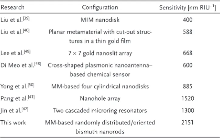
In contrast to the broadband absorbers, some studies aim to design narrowband absorbers that have an absorbance peak at single resonance wavelength. Many different nano-pattern configurations were employed for achieving narrow-band absorbers that are highly sensitive to the changes in the dielectric properties of their surroundings.[39–48] Liu et al. designed an MIM nanodisk narrowband perfect absorber with a sensitivity of 400 nm RIU−1 (refractive index unit).[39] They also developed a planar metamaterial that has cutout struc-tures in a thin gold film as an analog of an optically bright dipole antenna and an optically dark quadrupole antenna.[40] This metamaterial sensor that is based on coupling effects experimentally yielded a sensitivity of 588 nm RIU−1. Lee et al. designed 7 × 7 gold nanoslit arrays on a glass substrate that demonstrates a sensitivity of 668 nm RIU−1.[49] Di Meo et al. designed polarization insensitive cross-shaped plasmonic nanoantennas based a chemical sensor with a sensitivity of 600 nm RIU−1.[48] Yong et al. theoretically proposed a unit cell with four very close cylindrical nanodisk metal–metal (MM) architectures that can operate as a refractive index sensor with a sensitivity of 885 nm RIU−1.[50] Pang et al. designed a nanohole array surface plasmon resonance (SPR) biosensor that can reach 1520 nm RIU−1 sensitivity for certain cases.[41] Jin et al. demonstrated a highly sensitive integrated optical biosensor based on two cascaded microring resonators with a sensitivity of 1300 nm RIU−1.[42] Overall, not only is there room for improvement in the sensitivity, devices with more straightforward fabrication routes are also highly desirable. Last, but not the least, to the best of our knowledge, almost all of the designs in the literature function either as a broadband or narrowband absorber; so having each functionality in the same device remains a research problem.
In the present paper, we propose a facile fabrication route to realize a single bismuth (Bi) metal nanostructure–based, lithog-raphy-free double functional design that has ultra-broadband
absorption in the visible (Vis) and near-infrared (NIR) regimes, and narrowband absorption in the mid-infrared (MIR) regime. The designed structure is an MM configuration, which com-prises a thick planar bottom layer to block transmitted optical radiation and a top layer of disordered and densely packed nanorods. We utilize the finite-difference-time-domain (FDTD) method to numerically investigate the impact of geometrical parameters on the absorbance spectrum of the design, EMW confinement mechanism inside of the structure, and superi-ority of Bi over other metals. To explain the compatibility of Bi to broadband absorber designs, a systematic modeling approach is conducted. The transfer matrix method (TMM) is carried out to find the ideal permittivity region of the top layer, which is placed upon a thick metallic layer, for perfect absorption. In doing so, Bruggeman’s effective medium theory (EMT) is used to predict the effective permittivity of the metal nanorod–air composition for different metals such as nickel (Ni), chro-mium (Cr), gold (Au), tungsten (W), and Bi. We show that the extraordinary optical properties of Bi provide perfect absorp-tion with the widest bandwidth in the Vis and NIR ranges. The disordered and densely packed nanorods are produced by following a simple and lithography-free fabrication route, namely the oblique-angle deposition technique in a thermal evaporator system. We experimentally show that the proposed device achieves broadband absorbance nearly above 0.8 in Vis and NIR. Simultaneously, a narrowband absorbance resonance peak is attained at 6.54 µm, i.e., in the MIR range. To assess the suitability of this narrowband response for sensing applica-tions, we spin-coated poly(methyl methacrylate) (PMMA950K) onto the surface of the structure and the observed 1050 nm redshift in the resonance wavelength resulting in an ultrahigh experimental sensitivity of 2151 nm RIU−1. Overall, we unveil a new material (Bi) and demonstrate its superiority to other metals in applications that require strong light–matter interac-tions, namely highly sensitive refractive-index sensing in MIR, and at the same time ultra-broadband absorption in the Vis and NIR regimes.
2. Results and Discussion
2.1. Numerical Simulations
In an effort to scrutinize the impact of the parameters on absorbance performance and to understand the physical phe-nomena governing our device, numerical simulations were conducted for a simplified version of the fabricated sample using the commercial Lumerical FDTD Solutions software package. It is critical to mention that randomly distributed nanorods cannot be exactly modeled in the simulation region due to the random shape of the fabricated nanorods and unpre-dictable surface roughness. Therefore, we considered a simpler test device, whose schematic is shown in Figure 1a. This device comprises nanorods of radius R and length L that are periodic in two directions with a period, P. In this design, the incident electromagnetic radiation interacts with metallic nanorods and, consequently, it is diffracted into the metal nanorod–air com-position and excites several modes. These are mainly the longi-tudinal resonant modes among the nanorods because metallic
nanostructures elongated at one direction can support multiple longitudinal and transverse modes[34] which are mainly local-ized surface plasmon resonances (LSPRs). A nanorod in this structure can be considered as a monopole antenna where SPRs are excited at the Bi–air interface.
First, we investigated the role of the height of each nanorod,
L, on the absorbance spectrum, by sweeping L, while fixing R and P at 80 and 200 nm, respectively. As Figure 1b clearly
illustrates, the proposed nanoantenna has multiple longi-tudinal modes that appear as straight lines. For L < 200 nm, only the dominant mode is excited (which is the first-order longitudinal mode) and near unity absorbance is acquired in a narrow spectral range. As the rod length becomes larger, multiple absorbance modes are supported with the design and superposition of these modes leading to a broadband near unity absorbance, which are in line with the previous Figure 1. Parameter effect and modeling. a) The perspective view of the unit cell of designed two-layered structure. b) Contour plot of absorbance for the length parameter. c) Sweep and optimization of L from 50 to 400 nm while P = 200 nm and R = 80 nm. d) Contour plot of absorbance for radius parameter. e) Sweep and optimization of R from 20 to 90 nm while P = 200 nm and L = 300 nm. f) Absorbance performance comparison of Bi with Au, Cr, Ni, and W in FDTD simulation. g) Real and h) imaginary parts of the permittivity of the given materials. i) Generalized case of designed MM structure with a thick Al layer as a common reflector and an effective medium of metal nanorod–air composition. Contour plot of reflection of the structure in panel (i) and effective permittivity of the upper layer as a dot at the wavelengths of j) λ = 2 µm, k) λ = 3 µm, l) λ = 4 εm. In panels (j)–(l),
findings.[34] Moreover, the absorbance strength continuously grows stronger with increasing nanorod lengths as expected because the excited modes are mainly longitudinal modes, and new modes are excited with increased nanorod lengths. Furthermore, a slight redshift of the resonance wavelengths occurs in longer nanorods. It is clearly seen in Figure 1c that lower order modes (resonances at longer wavelengths) have weaker absorbance peaks at resonances of higher order modes (resonances at shorter wavelengths) because as the order of modes is increased, the modes get closer and the coupling between them becomes stronger. At sufficiently high values of
L, the absorbance profiles of different modes overlap with each
other and, therefore, absorbance approaches unity. When it is increased too much, however, their overlap decreases because of the different amount of redshift that occurs for different res-onances. Therefore, the optimal L value was chosen as 300 nm to have a fair trade-off between the absorbance amplitude and bandwidth.
Another critical design parameter is the rod’s transverse dimension, which is R. For this plot, L and P are each fixed at 300 and 200 nm, respectively, and R is swept. Figure 1d shows the resonance modes for different radius values. When nanorods have a small radii, absorbance performance is quite poor because of the low packing density, in other words, the large gap distances between neighboring nanorods. In fact, the response is mainly originated from the bulk absorbance of the Bi bottom plate. As the radius increases (or correspondingly the gap distances are reduced), the dominant peak becomes stronger and shifts to longer-wavelength values, which is also observed in Figure 1e. According to previous studies, the EMW confinement in deep subwavelength nanogaps can cause a spectrally narrow EMW absorption.[51] In addition, as the gap reduces, this absorption peak experiences a redshift. These are in line with our findings. When the packing density is higher, the strong field localization between the nanorods and the cou-pling of incident radiation to the low Q-factor LSPRs, due to the lossy nature of Bi, lead to perfect EMW harvesting in a broad-band wavelength regime, when the packing density is high.
However, a disparate phenomenon is observed in the shorter wavelengths. The high packing density will turn this nanostruc-ture design into a semimirror bulky strucnanostruc-ture and, therefore, the absorbance in shorter wavelengths will be diminished. Therefore, a wise design should have multiple gap sizes to cover both spectral regions. To find an optimum size, we pre-ferred to choose the largest bandwidth with at least 0.7 absorb-ance to have satisfying absorptive properties in the Vis and NIR regions; therefore, we continued to have simulations with a radius of 80 nm.
Despite the fact that it is difficult to obtain a broadband perfect absorber with an MM structure, since metals are reflective due to their high refractive indices at the Vis and infrared regimes, our results demonstrate that the proposed Bi-based MM structure has a remarkably strong absorb-ance response. Such a strong absorbabsorb-ance in an MM struc-ture can then be attributed to the excellent optical properties of Bi. To prove this argument and to compare Bi with other common metals, the optimum absorbance of the MM struc-ture for each different metal was extracted by simulating them with the above-mentioned strategy. The comparison of these
metals with Bi is shown in Figure 1f. This figure reveals the superior absorbance performance of Bi in comparison with the lossy metals, such as Cr, Ni, W, and Au (a noble metal). While these metals, except for Au, show a similar absorbance spectrum up to 2 µm, Bi maintains its performance in the NIR and MIR regimes, although the absorbance of the other metals decreases abruptly to the levels as low as 0.3. Such an outstanding absorbance performance arises from the unique optical property (i.e., permittivity) of Bi. Although Bi and other metals share a similarity in terms of the imaginary part of their corresponding permittivities (see Figure 1g), the dis-persion of the real part of the permittivity of Bi is completely different than the other metals, as shown in Figure 1h. The real part of the complex permittivities of Bi and other metals are close to each other up to 2 µm, similar to their absorb-ance performabsorb-ance in Figure 1f. Nevertheless, the real part of the permittivities of other metals abruptly decreases to large negative values after 2 µm, whereas the real part of the per-mittivity of Bi assumes positive values. It is this distinctive feature of Bi that enables the Bi-based MM absorber to have a significantly better performance compared to the absorbers with other metals for wavelengths larger than 2 µm. In fact, bismuth acts as a plasmonic metal in shorter wavelengths and a lossy dielectric in longer wavelengths.
To further emphasize the importance of having positive values of the real part of the permittivity in designing broad-band absorbers, we conducted a systematic study to antici-pate the absorbance performance of different materials in the designed MM structure. We generalized the problem in theo-retical modeling by using a thick Al layer as a commonly used perfect mirror in the bottom layer and a composition of metallic nanorods and air in the top layer, as shown in Figure 1i. We employed TMM to find the total reflection from the design. From these data, we sought for the ideal material that yields minimal absorbance upon being used in a metal–air composite structure.
In this method, we suppose the structure is bounded with a material of εA which, in our case, is air. For the transverse mag-netic (TM) polarization, Hy can be expressed as
e e , 0 e e , 0 e e , e , i r i 1 i 2 i 1 i 2 i M t i M A A C C M M S M H z A A z C C z L M M L z D L S z D L y i k z k z k z k z k z L k z L k z D L
( )
= + < + < ≤ + < ≤ + > + ( ) ( ) ( ) − − − − − − − (1)where z = 0 plane is the interface between metal nanorod– air composition and air, Ai, M1, and C1 are coefficients of the propagating waves in the +z-direction (i.e., from air to sample) and Ar, M2, and C2 are coefficients of the propagating waves in the −z-direction (i.e., from sample to air) in media of air, thick metallic layer, and metal nanorod–air composition, respectively.
St is the coefficient of the propagating waves in the +z-direction inside the substrate; however, it is zero due to a thick metallic layer. DM and L are the thickness of the bottom thick planar metallic layer and upper metal nanorod–air composition layer, respectively. kA, kC, kM, and kS are propagation constants in air, metal nanorod–air composition, thick metallic layer, and substrate, respectively. Applying the appropriate boundary
conditions, the reflection of the incident electromagnetic radiation from the structure can be obtained as R F
F 11 12 2 = . Here, 11 12 1 1 1 21 1 211, F F F a c c m m s = = − − − where 1 1 i i , 1 i 1 A A A A 1 s s a k k s k ε ε ε = − = (2a) 1 1 i i , e e i e i e 1 C C C C 2 i i C i C C i C C C C C c k k c k k k L k L k L k L ε ε ε ε = − = − − − (2b) 1 1 i i , e e i e i e 1 M M M M 2 i i M i M M i M M M M M M M M M m k k m k k k D k D k D k D ε ε ε ε = − = − − − (2c) and ( A,C,M,S) 2 2 2 k c k
i= = ε ωi − x where c is the speed of light, kx is the propagation constant in the x-direction, and εA, εM, εC, and εS represents permittivity of air, thick metallic layer (Bi), metal nanorod–air composition, and silicon (Si) substrate, respectively. By adopting this method, the contour plot of reflection depending on the real and imaginary parts of the permittivity of metal–air composite at a specific wavelength can be obtained, as shown in Figure 1j–l. While using TMM, we replaced the metallic nanodisks with an effective medium that is made of metal and air fillings. Therefore, we need to know the effective permittivity of the metal–air composite medium to complete the modeling of the designed structure. We can then determine the overall reflection from the whole structure by looking at where effective permittivity of the upper layer falls on this plot.
In converting the metal–air composite to a planar effective medium with an effective permittivity (εeff), we put Bruggeman’s EMT into use. It is crucial to mention that this model is accurate if the dimensions of the metal inclusions are much smaller than the wavelength. Our main goal, however, is to obtain an insight into the differences between the various metals in terms of their compatibility to be used in the metal–air composite, rather than having precise reflection values. Based on the Bruggeman’s theory, εeff is calculated according to the formula of
1 4 3 1 3 1 3 1 3 1 8 eff 1 1 2 2 1 1 2 2 2 1 2 f f f f ε = ( − )ε +( − )ε ± ( − )ε +( − )ε + ε ε (3) where f1 and f2 are filling factors of Bi nanorods and air, and ε1 and ε2 are permittivities of Bi and air, respectively. The sign of the square root is chosen in such a way that the imaginary part of the effective permittivity is positive due to causality in any passive medium. The permittivity data of Bi were extracted using a J. A. Woollam Co. Inc. V-VASE and IR-VASE ellipsom-eter in the wavelength range of 0.3–10 µm, and permittivities of Au, Cr, W, and Ni were taken from the database of Lumerical FDTD Solutions.
The calculated effective permittivity values for all of these materials are projected as black dots onto the reflection contour
plots in Figure 1j–l. In this figure, the blue semicircles are per-mittivity values that lead to a reflection below 0.3 (or equiva-lently an absorbance above 0.7). At a wavelength of 2 µm, Bi and Cr are located in the vicinity of this ideal circle. However, for larger wavelengths, these blue regions correspond to the areas that require large positive real permittivities. In fact, at a 4 µm incident EMW wavelength, only the effective permittivity of Bi is located in the close proximity of the perfect absorption circle. Thus, any composition of a metal other than Bi (with a permittivity that has a negative real part) and air (whose permit-tivity is 1) cannot satisfy this ideal condition. However, Bi, with a positive real permittivity, can satisfy this matching condition upon finding the proper disk dimensions. Therefore, this veri-fies the aforementioned uniqueness of the optical response of the Bi layer to achieving ultra-broadband EMW absorption in an MM design configuration.
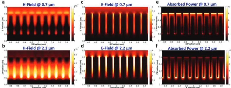
To better understand the nature of the excited modes and how optical radiation is confined inside the nanorods at the resonance wavelength, electric (E-field) and magnetic (H-field) plots, and absorbed power graphs are shown in Figure 2a–f at two different wavelengths of 0.7 and 2.2 µm that correspond to the positions of absorbance peaks. When the structure is con-sidered from a monopole antenna standpoint, multiple surface plasmon polaritons (SPPs) at different wavelengths are excited at the Bi–air interface. The excited resonant plasmon modes confine the H-field of the incident EMW mostly at the top of the nanorods at shorter wavelengths depending on the order of the modes. At the Vis region, the material properties become the dominant factor in determining the overall reflection from the structure. Near-ideal index matching between Bi nanorod– air composition and the environment (i.e., air) results in absorption at the interfaces. At longer wavelengths, small gaps between adjacent nanorods result in stronger field localiza-tion due to the interaclocaliza-tion between metallic nanostructures.[51] Thus, incident H-field is mostly confined at the bottom of the nanorods and very small gaps, as shown in Figure 2a,b. E-field is mainly localized at the gaps along the nanorods, as shown in Figure 2c,d. From Figure 2e,f, it can be seen that optical energy is mostly confined and harnessed at the top edges of the nanorods at 0.7 µm while this energy is localized around the side walls at the bottom of the nanorods at 2.2 µm. The EMW confinement region is observed to shift into the bottom parts of the nanorods and become stronger with an increasing wavelength. It can be inferred from the resemblance between the H-field and absorbed power localization regions that the structure exhibits magnetic dipole characteristics.
Our discussions up to this point have indicated the extraor-dinary absorbance response of Bi metal. It is demonstrated that a strong absorbance can be acquired in a periodic pattern of Bi nanostructures in an MM configuration. Sub-stantial improvement in absorbance can be accomplished by introducing a disorder into the geometries of the design. It was shown that the changes in L and R are an effective tool in manipulating the spectral position and strength of the absorbance peak. This randomness can be applied not only to the geometrical parameters but also to the orientation of nanorods. In such an architecture, multiple absorbance peaks can be superposed to achieve an overall flat, perfect absorbance throughout an ultra-broadband wavelength regime.
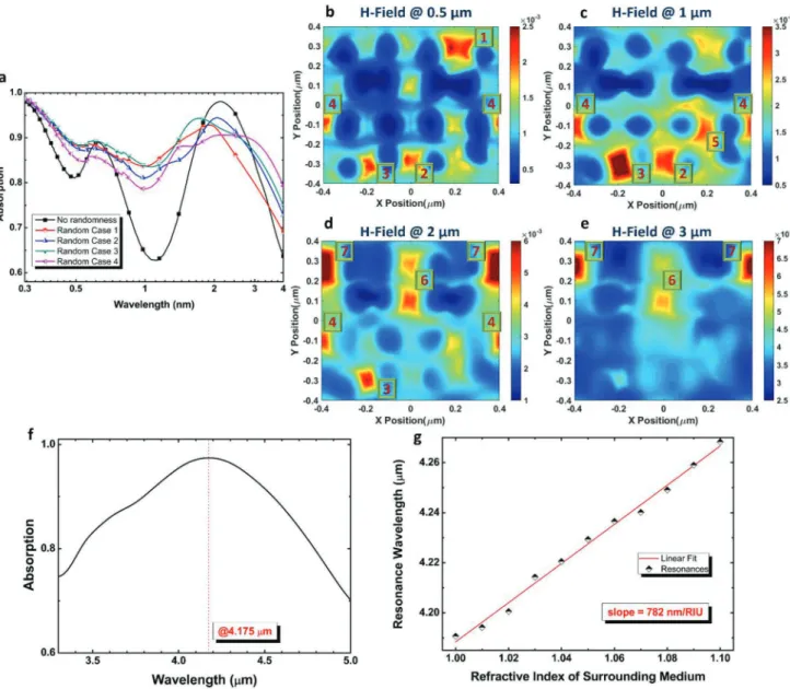
To test the validity of this, we carried out simulations by ran-domizing the nanorods. For this purpose, we designed a unit cell containing 16 nanorods with random design geometries. Using the random number generator function of the Lumer-ical software, nanorods were rotated around the x- and y-axes for a random value between −30° and 30°. We also added 10% tolerance to the radius and length of the nanorods (i.e., R can take a value between 72 and 88 while L can take a value within 270 and 330). Using this approach, the absorbance profiles of four different random combinations were compared with a periodic design, as shown in Figure 3a. As this figure clearly highlights, when the structure has such random geometries, it achieves broader and stronger absorbance compared to the periodic structure. In addition, different randomness scenarios reveal distinct absorbance spectra in which the minimum value may differ for a value around 0.1 (while random case 1 has minimum absorbance around 0.68, random case 4 reveals minimum absorbance around 0.78). Although the simulated random 16 nanorod unit cell is eventually a periodic structure, the fabricated sample simultaneously includes many different combinations of randomly grown nanorods. Therefore, the simultaneous utilization of the unique optical response of Bi and the proposed randomness can lead to a flat perfect absorb-ance in an ultra-broadband range.
To better explain this, the H-field profiles of the unit cell comprise 16 random nanorods as shown in Figure 3b–e, on which localized light confinement regions are numbered. It can be inferred from these panels that, at four different wave-lengths, there is a circulation of resonance regions so that at least one mode is excited in the structure. In other words, the active regions of the MM structure are interchanged in dif-ferent wavelength values. For example, incident light with 0.5 µm wavelength excites four different modes in the unit cell, where 1 is the strongest light confinement region. At 1 µm, res-onant mode at 1 vanishes and a new mode is excited at 5 while the light is mostly confined at region 3, as shown in Figure 3c. At 2 µm, the new resonant modes are excited at regions 6 and 7 instead of modes at regions 2 and 5. It can be concluded from
these field profiles that the proposed random structure can sup-port multiple modes in different wavelength values. Thus, there are always excited resonance modes in the structure; and this in turn leads to a broadband absorbance of the incident light.
In addition to the broadband absorbance profile of the proposed design in Vis and NIR, the MIR response of the periodic Bi nanorods was analyzed, and numerical analysis yielded a narrow resonance peak was also noted at 4.175 µm, as shown in Figure 3f. In plasmonic narrowband absorbers,[52–56] where the absorption is achieved via excitation of SPR in the metal–dielectric interface, the change in the index of the sur-rounding medium can cause a shift in the absorption peak. This redshift of the resonance, induced by an increase in the refractive index of the dielectric environment, is widely utilized for sensing applications. The sensing capability of a design is usually described by the term of sensitivity, which is defined as
S n λ = ∆
∆ where S, Δλ, and Δn are sensitivity, shift in resonance
wavelength, and change in refractive index of the surrounding medium on the surface, respectively. To demonstrate the sensing performance of this design, the refractive index of the environment was varied from 1 to 1.10 with a step interval of 0.01, and the corresponding new resonance wavelengths are shown in Figure 3g, where a notable redshift of resonance is observed. The sensitivity is measured from the slope of the line that is attained by linearly fitting the peak spectral positions of the resonances. It is calculated as 782 nm RIU−1, which is on par with the other reported values.
2.2. Fabrication
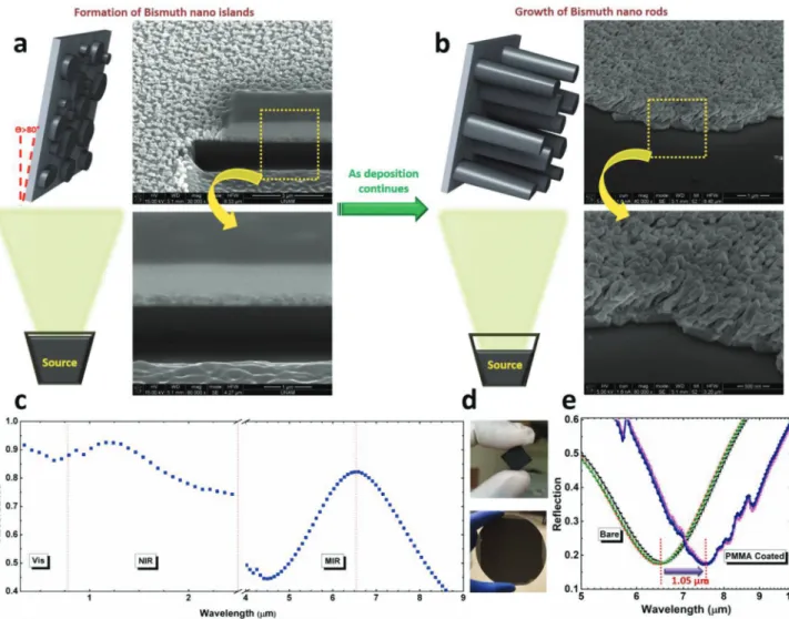
Although the oblique-angle deposition method is commonly used to fabricate the sidewall coatings of the edges or grat-ings,[57–60] we propose to use this method to fabricate disordered and densely packed nanorods by utilizing self-shadowing effect of the primarily grown nanoislands. Samples have been fab-ricated using the thermal evaporator equipment in two steps. Figure 2. Field Profiles. H-field profiles at a) 0.7 µm and b) 2.2 µm. E-field profiles at c) 0.7 µm and d) 2.2 µm. Absorbed power profiles at e) 0.7 µm and f) 2.2 µm.
In the first step, a simple thick planar Bi layer was coated in the ordinary manner, on a Si wafer to constitute the basement for nanorods and to act as a back-reflecting mirror. In the second step, oblique-angle deposition along with the aforementioned shadowing effect was exploited and the desired structure was realized. As illustrated in Figure 4a, the sample was positioned at a few degrees incline with respect to the vertical axis; there-fore, the coating was realized with a bottom-up approach. Although evaporated gas molecules are grown in every part of the sample at the beginning of the evaporation process, as the deposition continues, the initially grown nanorods pre-vent the growth of the nanostructures behind them, due to the shadowing effect. At the early steps of the coating, nano-islands of short Bi nanorods came into existence with a random
distribution, as demonstrated in the scanning electron micro-scope (SEM) image of the fabricated sample in Figure 4a. As the evaporation continued, nanoislands were elongated in one direction and densely packed Bi nanorods emerged, as shown in the cross-sectional view of the Bi nanorods in Figure 4b. It should be noted that elongated nanorods are separated by small gap distances and they preserve their shape although increasing the evaporation time. The proposed route that con-sists of two straightforward deposition steps allows for a large-scale compatible and high-throughput fabrication route to realize randomly distributed nanorods with high packing den-sity. Moreover, the length of the nanorods can be adjusted by controlling the deposition time. The details of the fabrication are given in the “Experimental Section”.
Figure 3. Effect of randomness on absorbance performance and EMW confinement mechanism. a) Absorbance spectra of 16 nanorod unit cell when nanorods have no orientation and different random scenarios. H-field profile of the unit cell at the middle height of the nanorods at wavelengths of b) 0.5 µm, c) 1 µm, d) 2 µm, and e) 3 µm. f) Simulated absorbance spectrum for the range of 3.2–5 µm. g) Resonance wavelengths for different sur-rounding medium refractive index values and linear fit in order to find the sensitivity of the sensor.
2.3. Characterization Results
Two samples were fabricated using the proposed technique. One sample has a thickness of 300 nm to measure the perfor-mance of the design, while the other has 600 nm to obtain the cross-sectional SEM image. The reflection spectra of the fabri-cated samples were acquired in the range of the Vis and NIR regions using a total reflection spectrophotometer that con-tains an integrated sphere setup to account for the significant scattering effect that we observed due to disordered nanorods at the sample surface. The details of the optical characteriza-tion are given in the “Experimental Seccharacteriza-tion”. Since there is no transmission in our design due to a thick metallic bottom layer, measuring only the reflection suffices to determine the absorption inside the structure, by using the formula A = 1 − R. The measurement results demonstrate broadband absorb-ance above 0.85 in Vis (from 0.3 to 0.78 µm) and above 0.75 in the whole NIR regime (from 0.78 to 2.5 µm), as shown in
Figure 4c. It should be noted that the average absorbance in this bandwidth (0.3–2.5 µm) is 0.8498, and the background absorb-ance beyond this bandwidth (2.5–11 µm) is 0.5172. This stems from the fact that the optical properties of Bi provide a good impedance matching from air to the metal–air composite; and, therefore, such a high absorbance is attained in Vis–NIR. As explained in the theoretical section, Bi is the only metal whose effective permittivity in this design stays in the vicinity of the ideal absorption region; however, it moves away from the ideal region with an increasing wavelength. On the other hand, small gaps between densely packed metallic nanorods, as shown in Figure 4b, result in a stronger localized field at longer wave-lengths. The incident light is efficiently confined at the metal/ air interface and between the small gaps in the NIR regime. The image of the fabricated small-area sample, from which all of the measurements are taken, is shown in Figure 4d. This figure also shows a proof-of-concept 4 in. silicon wafer fabricated with the proposed method to demonstrate the large-scale compatibility. Figure 4. Fabrication and characterization results. a) Early steps of the oblique-angle deposition technique to create Bi nanoislands. b) Transforma-tion of nanoislands into the nanorods as deposiTransforma-tion continues. c) Absorbance spectra in all regions (Vis, NIR, and MIR) of the fabricated sample. d) Narrow band absorbance of the bare and PMMA-coated samples, and the associated spectral shift of resonance for refractive index sensing. Insets 1 and 2 of panel (c) show the fabricated small-area sample and 4 in. silicon wafer, respectively.
The fabricated sample was characterized using the Fourier transform infrared spectroscopy (FTIR) technique in the MIR regime. The reflection spectrum of the sample was measured from several different positions to attain an average response. As a result, a narrowband absorbance centered on 6.54 µm was attained, as shown in Figure 4c. To test the sensing capability of the fabricated sample, PMMA950K was selected as the sensing target because its complex refractive index has constant real part and zero imaginary part (i.e., zero absorbance) in the range of 4–10 µm. The 200 nm thick PMMA was spin-coated on the ran-domly distributed Bi nanorods, and the resulting absorbance response was characterized by using FTIR. The reflection spectra of bare and PMMA-coated Bi nanorods are plotted in Figure 4e. As shown in the figure, the resonance wavelength is shifted from 6.54 to 7.59 µm in the amount of 1.05 µm due to PMMA. The sensitivity of the design is calculated as S = 2151 nm RIU−1. The sensitivity of this design is significantly larger than what was previously reported in the literature, as shown in Table 1. The ultra-high-sensitive response of the structure to a change in refractive index arises because designs that set up strong inter-action between the sample and the resonant mode have high sensitivity.[61] As explained in the field-confinement mechanism, the incident light is mainly coupled to the SPP modes excited at the Bi/air interface, and small gaps between metallic nanorods substantially improve the field localization at longer wavelengths. Tiny changes in the refractive index of the dielectric environment around nanorods naturally affect both the excited modes and interactions between metallic nanostructures. When a material with a different refractive index (PMMA in this case) is replaced
with air, the modified nature of the coupling effects causes a redshift in the resonance. Thus, a refractive index sensing with ultrahigh sensitivity is experimentally realized.
We also experimentally compared Bi with Au (a noble metal) and Cr (a lossy metal that is seen to be the second most appro-priate metal for broadband absorption, according to the analysis in the “Numerical Simulations” section) in both the Vis–NIR regimes and MIR regime. The absorbance spectra for each MM structure that employs different metals are shown in Figure 5a. For all of the samples, the thickness of the top layer (L) that consists of disordered and densely packed nanorods was chosen as 300 nm. For gold, similar results are obtained with Table 1. Literature review for sensitive narrowband absorbers.
Research Configuration Sensitivity [nm RIU−1]
Liu et al.[39] MIM nanodisk 400
Liu et al.[40] Planar metamaterial with cut-out
struc-tures in a thin gold film
588 Lee et al.[49] 7 × 7 gold nanoslit array 668
Di Meo et al.[48] Cross-shaped plasmonic nanoantenna–
based chemical sensor
600 Yong et al.[50] MM-based four cylindrical nanodisks 885
Pang et al.[41] Nanohole array 1520
Jin et al.[42] Two cascaded microring resonators 1300
This work MM-based randomly distributed/oriented bismuth nanorods
2151
Figure 5. a) Experimental comparison of the absorbance spectra for MM structures that comprise Bi, Au, and Cr. b) Absorbance spectra for different Bi samples with different top-layer Bi thicknesses. c) Reflectance spectrum of Bi nanorods at room temperature just after deposition, after 10 days passed and after kept under 100° for 24 h. d) XRD result for the fabricated Bi sample with L = 300 nm.
respect to the simulations, in the sense that it yields a very low absorbance in the NIR range, which is much poorer than both Bi and Cr. A comparison of Bi and Cr shows that both metals are very efficient Vis–NIR absorbers, and their average absorb-ance is close to each other because between 700 nm and 1.7 µm bismuth outperforms Cr, while the opposite is true for the wavelength interval of 1.7–2.5 µm. Nevertheless, unlike Bi, Cr shows no distinct resonance in the MIR range, so it is not a suitable metal to be used in a double-functional device. Next, we tried to experimentally validate our arguments about the effect of L on the absorbance spectrum. For this aim, in addition to the sample whose characterization is discussed up to this point (whose L is 300 nm), we fabricated three more samples with
L = 120 200 400 nm. We then characterized the absorbance
spectra of all four devices in the Vis and NIR ranges, and the results are plotted in Figure 5b. A comparison of the absorb-ance spectra of all four devices shows that as L is increased, the overall absorbance, most notable in the NIR range, becomes stronger, which is fully consistent with the simulation result in Figure 1b,c. The same analysis could not be carried for the
R and P, due to the inherent lack of control on these
parame-ters, in other words, because those dimensions are determined randomly during the nanoisland formation and the consequent deposition where shadowing is operative.
For practical applications of our proposed devices, the damage threshold is an important consideration. The broad-band perfect absorption of our device in the Vis and NIR ranges would decrease its optical damage threshold compared to the bulk Bi, which is primarily limited by its low melting point. However, the bulky nature of Bi nanorods will help the con-duction of heat and keep the overall structure cooled. Because we did not have access to a high-power laser setup for testing the optical damage threshold of our sample and its long-term stability, we repeated our reflectance measurements 1) just after the deposition of Bi nanorods, 2) after storing in the ambient environment for 10 days, and 3) after annealing at 100 °C for 24 h. As shown in Figure 5c, the response is quite similar for all cases. Moreover, the crystallinity of the nanorod sample has been examined by X-ray diffraction (XRD). XRD analysis is carried out by Panalytical X’pert Multi-Purpose to identify the phase structure of the obtained sample, and the patterns have been collected in the range of 2θ = 20° −60° using Bragg–Bren-tano geometry (Cu Kα radiation, λ = 0.15418 nm). The spectra (Figure 5d) clearly reveal that the diffraction peaks match well with the powder X-ray diffraction pattern for hexagonal phased Bi (JCPDS Card No. 98-006-4703) with cell parameters
a = 4.546 Å and c = 11.86 Å.
3. Conclusion
In conclusion, we designed, fabricated, and characterized a single metal, lithography-free, double functional device which has ultra-broadband absorption in the Vis and NIR spectral ranges, while narrowband absorption in the MIR regime. The proposed metal–metal design experimentally performs broad-band absorbance above 0.85 in the Vis regime (0.3–0.78 µm) and above 0.75 in the whole NIR regime (0.78–2.5 µm) while it acts a narrowband absorber in the MIR range. The narrowband
plasmonic resonance in the MIR range is utilized for refractive index sensing, and an ultrahigh sensitivity of 2151 nm RIU−1 is experimentally obtained. We also numerically investigated our proposed device, by demonstrating the superior optical proper-ties of Bi compared to other metals. In addition, the utilization of oblique-angle deposition technique also allowed large-scale fabrication compatibility with high throughput. Overall, uti-lizing the exceptional optical response of Bi in our large-scale compatible devices resulted in achieving double functionality with significant performances for each. The obtained results and findings reveal the unprecedented potential of Bi nano-structures for a variety of applications including photoconver-sion and sensing.
4. Experimental Section
Fabrication of the Bismuth Nanorods: Briefly, first, a small-area,
square-shaped silicon substrate with 400 mm2 area was cleaned in
the sonication bath with acetone, isopropanol, and deionized (DI) water, each lasting 15 min, and then was dried with N2 flow. Next, the
surface was treated using oxygen plasma for 5 min. Cleaning of 4 in. wafers utilized the same procedure. Then, a 150 nm thick bismuth back-reflector was deposited by using a thermal evaporator system (MIDAS PVD 3T) at a chamber pressure of 3e-6–5e-6 Torr and at a rate of 3 Å s−1.
Lastly, the second bismuth layer with disordered and densely packed bismuth nanorods was coated in the same equipment with the same parameters, but with the rate of 9 Å s−1.
Optical Characterization: For the optical characterization of the
fabricated samples in the mid-infrared range, an FTIR microscope (Bruker-Vertex 70v, Hyperion microscope), with a numerical aperture of 0.4, in the range of 2.5–15 µm, was employed. The measurements in this range utilized a mid-infrared source, a KBr beamsplitter, and a nitrogen-cooled mercury–cadmium-telluride (MCT-D313) detector. A 125 nm gold-coated SiO2/Si substrate was used as a reference. In the
UV–Vis–NIR spectral ranges, optical characterization was carried out in the wavelength range of 300–2.5 µm, by making use of a commercial total reflection spectrophotometer (Agilent Cary 5000). The equipment operated a diffuse reflectance accessory (DRA) of a diameter of 110 mm, and white polytetrafluoroethylene (PTFE) was used as a reference.
Numerical Simulations: The designed structure was imitated as
periodic, neatly packed cylindrical nanorods with high packing density. The bottom metallic layer was in the xy plane, and the nanorods were elongated in the z-direction. A broadband plane-wave source, whose electric field was polarized in the x-direction (s or TM polarization), was placed above the structure with a distance of more than 4 µm. It should be noted that the polarization of the incident electromagnetic radiation does not have an influence on the absorbance performance because the design is symmetric in all directions, and thus, it is polarization insensitive. Periodic boundary conditions were employed in the x- and
y-directions while the perfectly matched layer (PML) was adapted in
the z-direction. Reflected and transmitted electromagnetic waves were collected using the power monitors at the top and bottom of the FDTD region. The absorption of the design was calculated by using the formula
A = 1 − R − T. Realizing that the bottom layer is a thick metal coating, it behaves as a reflecting mirror, and it is safe to neglect the amount of electromagnetic radiation that is transmitted through the design, and this was confirmed in the simulations. Therefore, the aforementioned formula was simplified to A = 1 − R.
Acknowledgements
The authors acknowledge financial support from Scientific and Technological Research Council of Turkey (TUBITAK) and DPT-HAMIT
under the Project Nos. 113E331, 114E374, and 115F560. One of the authors (E.O.) also acknowledges partial support from the Turkish Academy of Sciences (TUBA).
Conflict of Interest
The authors declare no conflict of interest.
Author Contributions
M.C.S. and A.G. contributed equally to this work. D.U.Y. assisted on fabrication and characterization. V.B.E. and E.O. supervised the research. All of the authors contributed to the discussion and report writing.
Keywords
bismuth, broadband absorbers, lithography-free fabrication, narrowband absorbers, ultrahigh sensitivity
Received: July 17, 2019 Revised: October 23, 2019 Published online: December 10, 2019
[1] P. Miao, L. F. Tam, N. Xie, J. Geom. Anal. 2017, 27, 1323. [2] Y. Li, L. Su, C. Shou, C. Yu, J. Deng, Y. Fang, Sci. Rep. 2013, 3, 2865. [3] E. Rephaeli, S. Fan, Opt. Express 2009, 17, 15145.
[4] C. Wu, B. Neuner, J. John, A. Milder, B. Zollars, S. Savoy, G. Shvets,
J. Opt. 2012, 14, 015002.
[5] W. Li, J. Valentine, Nano Lett. 2014, 14, 3510.
[6] N. I. Landy, S. Sajuyigbe, J. J. Mock, D. R. Smith, W. J. Padilla, Phys.
Rev. Lett. 2008, 100, 207402.
[7] Q.-Y. Wen, Y.-S. Xie, H.-W. Zhang, Q.-H. Yang, Y.-X. Li, Y.-L. Liu, Opt.
Express 2009, 17, 20256.
[8] K. Aydin, V. E. Ferry, R. M. Briggs, H. A. Atwater, Nat. Commun. 2011, 2, 517.
[9] F. Ding, J. Dai, Y. Chen, J. Zhu, Y. Jin, S. I. Bozhevolnyi, Sci. Rep. 2016, 6, 39445.
[10] Y. Lu, W. Dong, Z. Chen, A. Pors, Z. Wang, S. I. Bozhevolnyi, Sci.
Rep. 2016, 6, 30650.
[11] M. G. Nielsen, A. Pors, O. Albrektsen, S. I. Bozhevolnyi, Opt.
Express 2012, 20, 13311.
[12] A. Ghobadi, H. Hajian, M. Gokbayrak, S. A. Dereshgi, A. Toprak, B. Butun, E. Ozbay, Opt. Express 2017, 25, 27624.
[13] D. Hu, H.-Y. Wang, Q.-F. Zhu, J. Nanophotonics 2016, 10, 026021. [14] Q. Feng, M. Pu, C. Hu, X. Luo, Opt. Lett. 2012, 37, 2133.
[15] Y. Zhang, L. Zhou, J. Q. Li, Q. J. Wang, C. P. Huang, Sci. Rep. 2015,
5, 10119.
[16] H. Wang, L. Wang, Opt. Express 2013, 21, A1078. [17] W. Guo, Y. Liu, T. Han, Opt. Express 2019, 27, 5351.
[18] N. Mattiucci, M. J. Bloemer, N. Aközbek, G. D’aguanno, Sci. Rep. 2013, 3, 3203.
[19] A. Ghobadi, S. A. Dereshgi, H. Hajian, B. Bozok, B. Butun, E. Ozbay, Sci. Rep. 2017, 7, 4755.
[20] A. Ghobadi, H. Hajian, B. Butun, E. Ozbay, ACS Photonics 2018, 5, 4203. [21] A. Ghobadi, H. Hajian, A. R. Rashed, B. Butun, E. Ozbay, Photonics
Res. 2018, 6, 168.
[22] M. C. Soydan, A. Ghobadi, D. U. Yildirim, V. B. Erturk, E. Ozbay,
Plasmonics 2019, 14, 1801.
[23] A. Ghobadi, H. Hajian, M. C. Soydan, B. Butun, E. Ozbay, Sci. Rep. 2019, 9, 290.
[24] A. Ghobadi, H. Hajian, S. A. Dereshgi, B. Bozok, B. Butun, E. Ozbay, Sci. Rep. 2017, 7, 15079.
[25] A. Ghobadi, S. A. Dereshgi, B. Butun, E. Ozbay, Sci. Rep. 2017, 7, 14538. [26] Y. Zhang, T. Wei, W. Dong, K. Zhang, Y. Sun, X. Chen, N. Dai, Sci.
Rep. 2014, 4, 4850.
[27] A. Moreau, C. Ciracì, J. J. Mock, D. R. Smith, R. T. Hill, A. Chilkoti, Q. Wang, B. J. Wiley, Nature 2012, 492, 86.
[28] D. Pacifici, H. J. Lezec, L. A. Sweatlock, R. J. Walters, H. A. Atwater,
Opt. Express 2008, 16, 9222.
[29] L. Dal Negro, S. V. Boriskina, Laser Photonics Rev. 2012, 6, 178. [30] D. S. Wiersma, Nat. Photonics 2013, 7, 188.
[31] D. U. Yildirim, A. Ghobadi, M. C. Soydan, O. Atesal, A. Toprak, M. D. Caliskan, E. Ozbay, ACS Photonics 2019, 6, 1812.
[32] M. K. Hedayati, M. Javaherirahim, B. Mozooni, R. Abdelaziz, A. Tavassolizadeh, V. S. K. Chakravadhanula, V. Zaporojtchenko, T. Strunkus, F. Faupel, M. Elbahri, Adv. Mater. 2011, 23, 5410. [33] M. K. Hedayati, F. Faupel, M. Elbahri, Appl. Phys. A 2012, 109, 769. [34] A. Ghobadi, S. A. Dereshgi, H. Hajian, G. Birant, B. Butun, A. Bek,
E. Ozbay, Nanoscale 2017, 9, 16652.
[35] K. Bae, G. Kang, S. K. Cho, W. Park, K. Kim, W. J. Padilla, Nat.
Commun. 2015, 6, 10103.
[36] T. Stelzner, M. Pietsch, G. Andrä, F. Falk, E. Ose, S. Christiansen,
Nanotechnology 2008, 19, 295203.
[37] H. Fang, X. Li, S. Song, Y. Xu, J. Zhu, Nanotechnology 2008, 19, 255703.
[38] Y. J. Jen, Y. J. Huang, W. C. Liu, Y. W. Lin, Sci. Rep. 2017, 7, 39791. [39] N. Liu, M. Mesch, T. Weiss, M. Hentschel, H. Giessen, Nano Lett.
2010, 10, 2342.
[40] N. Liu, T. Weiss, M. Mesch, L. Langguth, U. Eigenthaler, M. Hirscher, C. Sönnichsen, H. Giessen, Nano Lett. 2010, 10, 1103. [41] L. Pang, G. M. Hwang, B. Slutsky, Y. Fainman, Appl. Phys. Lett.
2007, 91, 123112.
[42] L. Jin, M. Li, J. J. He, Opt. Commun. 2011, 284, 156.
[43] J. Jágerská, H. Zhang, Z. Diao, N. Le Thomas, R. Houdré, Opt. Lett. 2010, 35, 2523.
[44] K. V. Sreekanth, Y. Alapan, M. Elkabbash, E. Ilker, M. Hinczewski, U. A. Gurkan, A. De Luca, G. Strangi, Nat. Mater. 2016, 15, 621. [45] K. H. Yoon, M. L. Shuler, S. J. Kim, Opt. Express 2006, 14, 4842. [46] D. U. Yildirim, A. Ghobadi, E. Ozbay, Sci. Rep. 2018, 8, 15210. [47] D. U. Yildirim, A. Ghobadi, M. C. Soydan, M. Gokbayrak, A. Toprak,
B. Butun, E. Ozbay, J. Phys. Chem. C 2019, 123, 19125.
[48] V. Di Meo, A. Caporale, A. Crescitelli, M. Janneh, E. Palange, A. De Marcellis, M. Portaccio, M. Lepore, I. Rendina, M. Ruvo, E. Esposito, Sens. Actuators, B 2019, 286, 600.
[49] K.-L. Lee, C.-W. Lee, W.-S. Wang, P.-K. Wei, J. Biomed. Opt. 2007, 12, 044023.
[50] Z. Yong, S. Zhang, C. Gong, S. He, Sci. Rep. 2016, 6, 24063. [51] D. Ji, A. Cheney, N. Zhang, H. Song, J. Gao, X. Zeng, H. Hu,
S. Jiang, Z. Yu, Q. Gan, Adv. Opt. Mater. 2017, 5, 1700223.
[52] L. Meng, D. Zhao, Z. Ruan, Q. Li, Y. Yang, M. Qiu, Opt. Lett. 2014,
39, 1137.
[53] B. Zhang, Y. Zhao, Q. Hao, B. Kiraly, I.-C. Khoo, S. Chen, T. J. Huang, Opt. Express 2011, 19, 15221.
[54] Z. Li, S. Butun, K. Aydin, ACS Nano 2014, 8, 8242.
[55] Y. Chen, J. Dai, M. Yan, M. Qiu, Opt. Express 2014, 22, 30807. [56] F. Callewaert, S. Chen, S. Butun, K. Aydin, J. Opt. 2016, 18, 075006. [57] A. Kubo, Y. S. Jung, H. K. Kim, H. Petek, J. Phys. B: At., Mol. Opt.
Phys. 2007, 40, S259.
[58] J. C. Yang, H. Gao, J. Y. Suh, W. Zhou, M. H. Lee, T. W. Odom, Nano
Lett. 2010, 10, 3173.
[59] Y. J. Shin, C. Pina-Hernandez, Y. K. Wu, J. G. Ok, L. J. Guo,
Nano-technology 2012, 23, 344018.
[60] S. Giudicatti, S. M. Marz, L. Soler, A. Madani, M. R. Jorgensen, S. Sanchez, O. G. Schmidt, J. Mater. Chem. C 2014, 2, 5892. [61] I. M. White, X. Fan, Opt. Express 2008, 16, 1020.