Heavy photons at coupled-cavity waveguide band edges in a three-dimensional photonic crystal
Mehmet Bayindir*and E. OzbayDepartment of Physics, Bilkent University, Bilkent, 06533 Ankara, Turkey 共Received 10 April 2000兲
We report on measurements of delay time corresponding to evanescent coupled-cavity modes in three-dimensional photonic crystals. By creating a defect inside the crystal, photons are confined within a boxlike cavity of volume ⬃(/2)3. It is observed that photon lifetime increases drastically and group velocity of photons tends towards zero at the waveguiding band edges of the periodic coupled cavities. Experimental results are well explained within the classical wave analog of the tight-binding picture. Observation of the extremely small group velocity and long photon lifetime at the coupled-cavity waveguide band edges have important potential applications.
In the last several years, there has been much interest in physics and applications of spatially periodic dielectric or metallic structures, photonic band gap materials, which in-hibit propagation of the electromagnetic 共EM兲 waves within a certain range of wavelengths in all directions.1,2 The in-tense experimental and theoretical investigations continue on localization of light,3,4 tunneling phenomena in photonic systems,5–8 alteration 共i.e., inhibition and enhancement兲 of spontaneous emissions.9–11
By introducing a defect into a photonic crystal, photons with certain wavelengths can locally be trapped inside the defect volume, which is analogous to the localized impurity states in a semiconductor.12Recently, we experimentally and theoretically investigated splitting of the EM modes due to coupling between the evanescent cavity modes,13 and guid-ing and bendguid-ing of EM waves through periodic coupled cavi-ties in three-dimensional共3D兲 photonic crystals.14In this pa-per, we measure the delay time corresponding to localized cavity modes inside a 3D photonic crystal. We report on observation of heavy photons at the waveguiding band edges of the coupled-cavity array by measuring photon lifetime and group velocity of photons along the cavity array关Fig. 1共a兲兴. A formula for the photon lifetime is derived within the tight-binding共TB兲 formalism13,15–18that well describes the experi-mental results. For the two coupled-cavity case, it is also observed that photons in the antibonding mode spend more time inside the cavities compared to the bonding mode.
Heavy photons or photons with a extremely low group velocity play a critical role in enhancing the efficiency of nonlinear processes,21,20,17and gain enhancement in the pho-tonic band edge laser.19Moreover, the spontaneous emission rate can be increased since the effective gain is proportional to 1/vg.20 The low group velocity was proposed near the band edges of one-dimensional photonic band-gap structures.19,21Recently, Vlasov et al. have observed that the optical pulses significantly slow down at the 3D photonic crystal band edges in the visible spectrum.22
A layer-by-layer dielectric based photonic crystal23,24was used to construct the coupled cavities. The crystal consists of square shaped alumina rods having a refractive index 3.1 at the microwave frequencies and dimensions 0.32 cm⫻0.32 cm⫻15.25 cm. A center-to-center separation between the rods of 1.12 cm was chosen to yield a dielectric filling ratio
of ⬃0.26. The unit cell consists of four layers having the symmetry of a face-centered tetragonal共fct兲 crystal structure. The crystal exhibits a three-dimensional photonic band gap extending from 10.6 to 12.8 GHz.24,25
The experimental setup consists of a HP 8510C network analyzer and microwave horn antennas to measure the
FIG. 1. 共a兲 Schematics of propagation of photons through local-ized coupled-cavity modes within a photonic crystal. Amplitude of the strongly localized EM modes is enhanced inside each cavity, which leads to high Q factors and long lifetimep. The transit time is the sum of the escape rate of photons from the cavity (p) and the tunneling time between the cavities (t).共b兲 Experimental setup for measuring the transmission-amplitude and transmission-phase spec-tra of the coupled cavities in 3D photonic crystals. By removing some portion of a single rod, we can confine photons within a volume⬃(/2)3.
RAPID COMMUNICATIONS
PHYSICAL REVIEW B VOLUME 62, NUMBER 4 15 JULY 2000-II
PRB 62
transmission-amplitude and transmission-phase spectra 关Fig. 1共b兲兴. Removing some portion of a single rod from an oth-erwise perfect crystal leads to confined modes with high quality-factors, Q⫽⌬/0, around 1000.26Photons of
wave-length ⬃2.5 cm are confined within a very small volume order of VL⬃1 cm3. The electric-field polarization vector of the incident EM field was always parallel to the rods of the defect lines for all measurements.
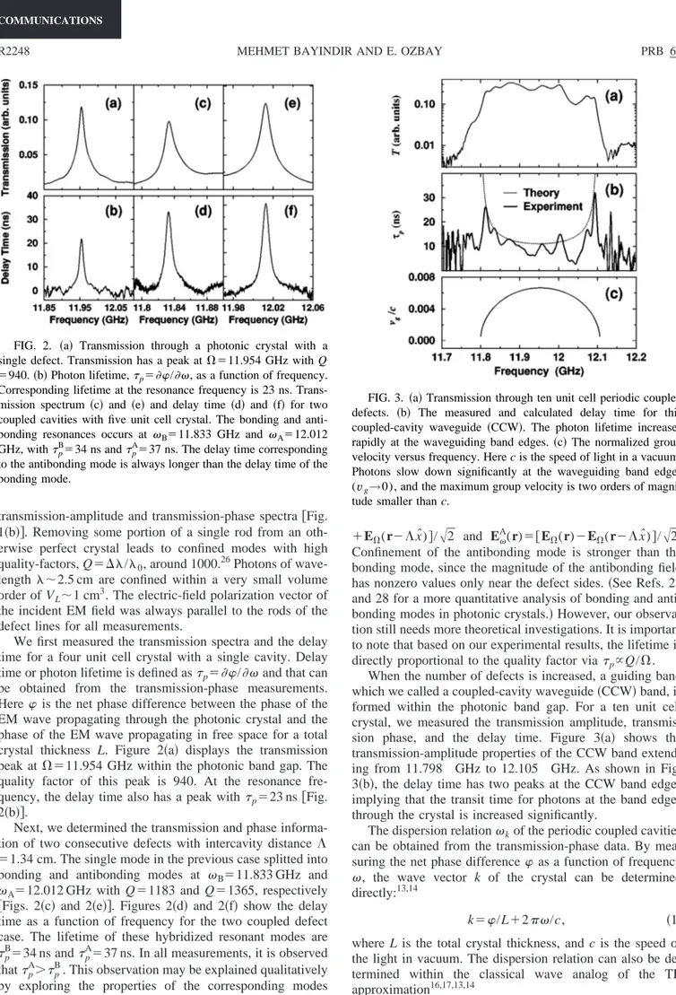
We first measured the transmission spectra and the delay time for a four unit cell crystal with a single cavity. Delay time or photon lifetime is defined asp⫽/and that can be obtained from the transmission-phase measurements. Here is the net phase difference between the phase of the EM wave propagating through the photonic crystal and the phase of the EM wave propagating in free space for a total crystal thickness L. Figure 2共a兲 displays the transmission peak at ⍀⫽11.954 GHz within the photonic band gap. The quality factor of this peak is 940. At the resonance fre-quency, the delay time also has a peak withp⫽23 ns 关Fig. 2共b兲兴.
Next, we determined the transmission and phase informa-tion of two consecutive defects with intercavity distance ⌳
⫽1.34 cm. The single mode in the previous case splitted into
bonding and antibonding modes at B⫽11.833 GHz and
A⫽12.012 GHz with Q⫽1183 and Q⫽1365, respectively
关Figs. 2共c兲 and 2共e兲兴. Figures 2共d兲 and 2共f兲 show the delay
time as a function of frequency for the two coupled defect case. The lifetime of these hybridized resonant modes are pB⫽34 ns andpA⫽37 ns. In all measurements, it is observed
thatpA⬎pB. This observation may be explained qualitatively by exploring the properties of the corresponding modes which can be written as the superposition of the individual cavity modes at each defect side EB(r)⫽关E⍀(r)
⫹E⍀(r⫺⌳xˆ)兴/冑2 and EA(r)⫽关E⍀(r)⫺E⍀(r⫺⌳xˆ)兴/冑2. Confinement of the antibonding mode is stronger than the bonding mode, since the magnitude of the antibonding field has nonzero values only near the defect sides.共See Refs. 27 and 28 for a more quantitative analysis of bonding and anti-bonding modes in photonic crystals.兲 However, our observa-tion still needs more theoretical investigaobserva-tions. It is important to note that based on our experimental results, the lifetime is directly proportional to the quality factor via p⬀Q/⍀.
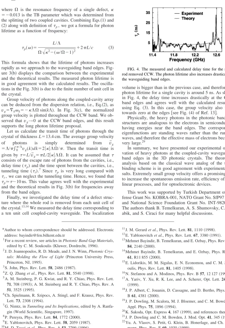
When the number of defects is increased, a guiding band which we called a coupled-cavity waveguide共CCW兲 band, is formed within the photonic band gap. For a ten unit cell crystal, we measured the transmission amplitude, transmis-sion phase, and the delay time. Figure 3共a兲 shows the transmission-amplitude properties of the CCW band extend-ing from 11.798 GHz to 12.105 GHz. As shown in Fig. 3共b兲, the delay time has two peaks at the CCW band edges implying that the transit time for photons at the band edges through the crystal is increased significantly.
The dispersion relationkof the periodic coupled cavities can be obtained from the transmission-phase data. By mea-suring the net phase difference as a function of frequency , the wave vector k of the crystal can be determined directly:13,14
k⫽/L⫹2/c, 共1兲
where L is the total crystal thickness, and c is the speed of the light in vacuum. The dispersion relation can also be de-termined within the classical wave analog of the TB approximation16,17,13,14
k⫽⍀关1⫹cos共k⌳兲兴, 共2兲
FIG. 2. 共a兲 Transmission through a photonic crystal with a single defect. Transmission has a peak at⍀⫽11.954 GHz with Q ⫽940. 共b兲 Photon lifetime,p⫽/, as a function of frequency.
Corresponding lifetime at the resonance frequency is 23 ns. Trans-mission spectrum 共c兲 and 共e兲 and delay time 共d兲 and 共f兲 for two coupled cavities with five unit cell crystal. The bonding and anti-bonding resonances occurs at B⫽11.833 GHz andA⫽12.012
GHz, withp
B⫽34 ns and
p
A⫽37 ns. The delay time corresponding
to the antibonding mode is always longer than the delay time of the bonding mode.
FIG. 3. 共a兲 Transmission through ten unit cell periodic coupled defects. 共b兲 The measured and calculated delay time for this coupled-cavity waveguide 共CCW兲. The photon lifetime increases rapidly at the waveguiding band edges.共c兲 The normalized group velocity versus frequency. Here c is the speed of light in a vacuum. Photons slow down significantly at the waveguiding band edges (vg→0), and the maximum group velocity is two orders of
magni-tude smaller than c.
RAPID COMMUNICATIONS
where ⍀ is the resonance frequency of a single defect,
⫽⫺0.013 is the TB parameter which was determined from
the splitting of two coupled cavities. Combining Eqs.共1兲 and
共2兲 along with definition ofp, we got a formula for photon lifetime as a function of frequency:
p共兲⫽ L/⌳
⍀
冑
2⫺共/⍀⫺1兲2⫹2L/c 共3兲This formula shows that the lifetime of photons increases rapidly as we approach to the waveguiding band edges. Fig-ure 3共b兲 displays the comparison between the experimental and the theoretical results. The measured photon lifetime is in good agreement with the calculated results. The oscilla-tions in the Fig. 3共b兲 is due to the finite number of unit cell in the crystal.
Group velocity of photons along the coupled-cavity array can be deduced from the dispersion relation, i.e., Eq.共2兲, as vg⫽ⵜkk⫽⫺⌳⍀ sin(k⌳). In Fig. 3共c兲, the normalized group velocity is plotted throughout the CCW band. We ob-served that vg→0 at the CCW band edges, and this result supports the long photon lifetime proposal.
Let us calculate the transit time of photons through the crystal of thickness L⫽13.4 cm. The average group velocity of photons is simply determined from ¯vg
⫽⌳/兰0/⌳vg(k)dk⫽2兩兩⌳⍀/. Then the transit time is given by ⫽L/v¯g⫽L/2兩兩⌳⍀. It can be assumed that consists of the escape rate of photons from the cavities, i.e., delay time (p) and the time spent between the cavities, i.e., tunneling time (t).7 Since p is very long compared with t, we can neglect the tunneling time. Hence, we found that p⯝⬃10 ns. This value agrees well with the experimental
and the theoretical results in Fig. 3共b兲 for frequencies away from the band edges.
Finally, we investigated the delay time of a defect struc-ture where the whole rod is removed from each unit cell of the crystal.13,14We measured the delay time corresponding to a ten unit cell coupled-cavity waveguide. The localization
volume is bigger than in the previous case, and therefore the photon lifetime for a single cavity is around 5 ns. As shown in Fig. 4, the delay time increases drastically at the CCW band edges and agrees well with the calculated result by using Eq. 共3兲. In this case, the group velocity also tends towards zero at the edges 关see Fig. 共4兲 of Ref. 13兴.
Physically, the heavy photons in the photonic band gap structures are analogous to the electrons in semiconductors having energies near the band edges. The corresponding eigenfunctions are standing waves rather than the running waves, and therefore the effective mass of electrons becomes very large.29
In summary, we have presented our experimental obser-vation of heavy photons at the coupled-cavity waveguiding band edges in the 3D photonic crystals. The theoretical analysis based on the classical wave analog of the tight-binding scheme is in good agreement with experimental re-sults. Extremely small group velocity offers a promising tool to increase the spontaneous emission rate, efficiency of non-linear processes, and for optoelectronic devices.
This work was supported by Turkish Department of De-fense Grant No. KOBRA-001, NATO Grant No. SfP971970, and National Science Foundation Grant No. INT-9820646. The authors thank B. Temelkuran, A. S. Shumovsky, C. Yal-abik, and S. Ciraci for many helpful discussions.
*Author to whom correspondence should be addressed. Electronic address: [email protected]
1For a recent review, see articles in Photonic Band Gap Materials, edited by C. M. Soukoulis共Kluwer, Dordrecht, 1996兲. 2J. D. Joannopoulos, R. D. Meade, and J. N. Winn, Photonic
Crys-tals: Molding the Flow of Light 共Princeton University Press, Princeton, NJ, 1995兲.
3S. John, Phys. Rev. Lett. 58, 2486共1987兲.
4Z. Q. Zhang et al., Phys. Rev. Lett. 81, 5540共1998兲.
5A. M. Steinberg, P. G. Kwiat, and R. Y. Chiao, Phys. Rev. Lett. 71, 708共1993兲; A. M. Steinberg and R. Y. Chiao, Phys. Rev. A 51, 3525共1995兲.
6Ch. Spielmann, R. Szipocs, A. Stingl, and F. Krausz, Phys. Rev. Lett. 73, 2308共1994兲.
7G. Nimtz, in Tunneling and Its Implications, edited by A. Ranfa-gin共World Scientific, Singapore, 1997兲.
8P. Pereyra, Phys. Rev. Lett. 84, 1772共2000兲. 9E. Yablonovitch, Phys. Rev. Lett. 58, 2059共1987兲. 10M. D. Tocci et al., Phys. Rev. A 53, 2799共1996兲.
11J. M. Gerard et al., Phys. Rev. Lett. 81, 1110共1998兲. 12E. Yablonovitch et al., Phys. Rev. Lett. 67, 3380共1991兲. 13Mehmet Bayindir, B. Temelkuran, and E. Ozbay, Phys. Rev. Lett.
84, 2140共2000兲.
14Mehmet Bayindir, B. Temelkuran, and E. Ozbay, Phys. Rev. B 61, R11 855共2000兲.
15E. Lidorikis, M. M. Sigalas, E. N. Economou, and C. M. Souk-oulis, Phys. Rev. Lett. 81, 1405共1998兲.
16N. Stefanou and A. Modinos, Phys. Rev. B 57, 12 127共1998兲. 17A. Yariv, Y. Xu, R. K. Lee, and A. Scherer, Opt. Lett. 24, 711
共1999兲. 18
J. P. Albert, C. Jouanin, D. Cassagne, and D. Bertho, Phys. Rev. B 61, 4381共2000兲.
19J. P. Dowling, M. Scalora, M. J. Bloemer, and C. M. Bowden, J. Appl. Phys. 75, 1896共1994兲.
20K. Sakoda, Opt. Express 4, 167共1999兲, and references therein. 21J. P. Dowling and C. M. Bowden, J. Mod. Opt. 41, 345共1994兲. 22Yu. A. Vlasov, S. Petit, G. Klein, B. Honerlage, and Ch.
Hirli-mann, Phys. Rev. E 60, 1030共1999兲.
FIG. 4. The measured and calculated delay time for the single rod removed CCW. The photon lifetime also increases drastically at the waveguiding band edges.
RAPID COMMUNICATIONS
23K. M. Ho, C. T. Chan, C. M. Soukoulis, R. Biswas, and M. M. Sigalas, Solid State Commun. 89, 413共1994兲
24E. Ozbay, J. Opt. Soc. Am. B 13, 1945共1996兲. 25
E. Ozbay and B. Temelkuran, Appl. Phys. Lett. 69, 743共1996兲. 26E. Ozbay, G. Tuttle, M. M. Sigalas, C. M. Soukoulis, and K. M.
Ho, Phys. Rev. B 51, 13 961共1995兲.
27M. I. Antonoyiannakis and J. B. Pendry, Europhys. Lett. 40, 613 共1997兲.
28M. I. Antonoyiannakis and J. B. Pendry, Phys. Rev. B 60, 2363 共1999兲.
29C. Kittel, Introduction to Solid State Physics, 7th ed.共John Wiley & Sons, New York, 1996兲, p. 209.
RAPID COMMUNICATIONS