Harmonic enhancement of Gunn oscillations in GaN
C. Sevik
∗, D. E. Yılmaz
∗and C. Bulutay
∗∗Department of Physics, Bilkent University, Bilkent, Ankara 06800, Turkey
Abstract. High field transport in wide bandgap semiconductors like GaN is of great technological importance. The negative differential mobility regime at high fields, under suitable conditions, can lead to millimeter-wave Gunn oscillations. Using extensive simulation based an ensemble Monte Carlo technique, the prospects of GaN Gunn diodes are theoretically investigated. The possibility of operating these Gunn diodes at their higher harmonic modes are explored. Main finding of this research is that the carrier dynamics in GaN can be tailored by an optimum choice of doping profile, temperature and bias conditions so that the efficiency of higher harmonic Gunn oscillations can be boosted.
INTRODUCTION
Gallium nitride with its high negative differential mo-bility threshold, measured [1] to be above 200 kVcm−1, is an appealing material for high power millimeter-wave Gunn diodes. An ever-present objective is to increase the operating frequency of the Gunn diodes, and a promis-ing approach is to operate them at their higher harmonic modes rather than their fundamental mode. In this work, our aim is to present a comprehensive ensemble Monte Carlo assessment of efficiency and harmonic enhance-ment in n-type GaN Gunn diodes, exploring the effects of including a doping notch/mesa, channel concentration, DC bias and the lattice temperature. We would like to ex-tract the trends rather than quantitative aspects so that our results can shed light on the physics of milimeter wave Gunn oscillations based on other materials as well.
STRUCTURAL DETAILS AND RESULTS
In the types of GaN-based Gunn structures we study, the overall active region length is always kept constant at a value of la= 1.2µm. This active region is sandwiched
between the heavily doped n+ regions with n+= 2 × 1018cm−3; the results were seen to be unaffected when this is increased to 1× 1019cm−3. The active region is composed of an active channel with a doping of n= 3× 1017 cm−3 (unless stated otherwise) and a lightly n-doped doping notch having n−= 1 × 1016 cm−3 or a doping mesa with n+= 5 × 1017cm−3.
The quantity of primary interest, oscillator efficiency, is defined as η = PAC/PDC, where PAC is the time-average generated AC power and PDC is the dissipated DC power by the Gunn diode. First, the effect of the
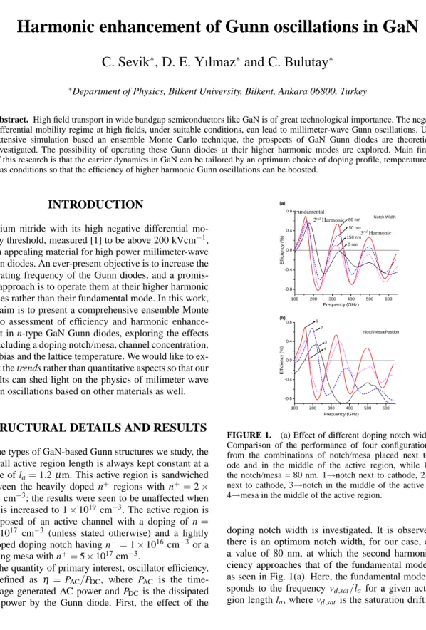
100 200 300 400 500 600 -0.8 -0.4 0.0 0.4 0.8 (a) Notch Width 0 nm 150 nm 50 nm 80 nm E ffi c ie n c y (% ) Frequency (GHz) Fundamental 2ndHarmonic 3rdHarmonic 100 200 300 400 500 600 -0.8 -0.4 0.0 0.4 0.8 (b) 4 3 2 1 Notch/Mesa/Position E ff icie n cy (% ) Frequency (GHz)
FIGURE 1. (a) Effect of different doping notch widths, (b) Comparison of the performance of four configuration made from the combinations of notch/mesa placed next to cath-ode and in the middle of the active region, while keeping the notch/mesa = 80 nm. 1→notch next to cathode, 2→mesa next to cathode, 3→notch in the middle of the active region, 4→mesa in the middle of the active region.
doping notch width is investigated. It is observed that there is an optimum notch width, for our case, around a value of 80 nm, at which the second harmonic effi-ciency approaches that of the fundamental mode value as seen in Fig. 1(a). Here, the fundamental mode corre-sponds to the frequency vd,sat/la for a given active
re-gion length la, where vd,sat is the saturation drift
veloc-231
CP772, Physics of Semiconductors: 27th International Conference on the Physics of Semiconductors,
edited by José Menéndez and Chris G. Van de Walle
ity. In the nth harmonic mode, there exist n Gunn do-mains travelling down the channel at each instant [3]. However, we would like to point out that the value of the optimum notch width is sensitive to the material pa-rameters and our previous analysis with the bandstruc-ture data of Ref. [4] resulted in a wider width [3]. On the other hand, a doping mesa rather than a notch was suggested to enhance the harmonic content of the cur-rent waveform [5, 6]. To elucidate this point, Fig. 1(b) compares the performance of four configurations made from the combinations of notch/mesa placed next to cath-ode and in the middle of the active region. It is seen that notch placed next to cathode (labelled as 1) performs the best among all. A source of curiosity regarding Fig. 1(b) is the substantial frequency shift for the notch placed in the middle (labelled as 3) and mesa placed next to the cathode (labelled as 2). Detailed investigation of these structures shows that for both cases almost half of the ac-tive region is inacac-tive in the domain nucleation processes hence remarkably decreasing the transit time of the Gunn domains. 100 200 300 400 500 600 70 80 90 100 110 120 130 Temperature (K) -0.5 0.0 0.5 1.0 20 (degree) (a) Notch = 80 nm, 60 V, 160 GHz E ffi c ie n c y (% ) φIV 100 200 300 400 500 600 -1.6 -1.2 -0.8 -0.4 0.0 0.4 0.8 Notch = 80 nm, 70 V (b) 5x10¹⁷ 1x10¹⁷ 3x10¹⁷ Frequency (GHz) Ef fi ciency (%)
FIGURE 2. (a) Temperature versus phase angle between the current and voltage waveforms, and efficiency; 80 nm-notch device at 60 V bias and its fundamental frequency (160 GHz) is used. (b) RF conversion efficiency versus frequency for channel dopings; 80 nm-notch device at 70 V DC bias is used.
Next, the effects of DC bias is investigated. While changing the applied DC voltage across the Gunn diode we need to scale the RF amplitude accordingly not to lose the grounds for efficiency comparison. The applied DC voltage has to be above a critical value so that the device is biased in the negative differential mobility regime. Ac-cording to our simulations (not shown), increasing bias has favorable effect on the fundamental and harmonic efficiencies. Another issue for high power Gunn diodes is thermal heating. At the expense of neglecting thermal
gradient effects, we simply consider the uniform lattice temperature effects on the efficiency. Based on our re-sults shown in Fig. 2(a), up to room temperature there is no sensible variation, whereas above the room temper-ature performance increasingly degrades becoming pas-sive above 480 K in the case considered. The source of this degradation is not due to a reduction in the oscilla-tion amplitudes but rather due to phase angle between the current and voltage waveforms shifting away from anti-phase (1800) to orthogonal (900) and to dissipative (00) as the temperature increases. The increase in the lattice temperature does not significantly shift the frequency but diminishes the efficiency globally. Therefore, good heat sinking is required in these GaN Gunn diodes. Finally, we investigate the effect of channel doping which is ob-served in Fig. 2(b) to be relatively, less influential on the fundamental mode efficiency than the higher harmonic modes, so that for a given notch width and bias voltage, there is an optimum channel doping that favors the har-monic enhancement. However, there is a lower threshold for the channel doping as it determines the dielectric do-main nucleation time that needs to be much shorter than the domain transit time through the active region [7].
CONCLUSION
In summary, we have analyzed the trends in efficiency and harmonic enhancement in GaN Gunn diodes under doping profile, bias and temperature variations. The key parameter in all these efficiency considerations has been the phase angle difference between the current and volt-age waveforms. Our extensive simulations indicate that the carrier dynamics in GaN can be tailored by an opti-mum choice of doping profile, temperature and bias con-ditions so that the efficiency of higher harmonic Gunn oscillations can be boosted.
REFERENCES
1. M. Wraback, H. Shen, J. C. Carrano, T. Li, J. C. Campbell, M. J. Schurman and I. T. Ferguson, Appl.
Phys. Lett.76, (2000), 1155.
2. G. M. Dunn and M. J. Kearney, Semicond. Sci. Technol. 18, (2003), 794.
3. C. Sevik and C. Bulutay, Semicond. Sci. Technol. 19, (2004), 188.
4. R. P. Joshi, S. Viswanadha, P. Shah, and R. D. del Rosario, Appl. Phys. 93, (2003), 4836.
5. S. H. Jones, G. B. Tait, and M. Shur, Micowave Opt.
Technol. Lett. 5, (1992), 354.
6. R. Judaschke, IEEE Trans. Microwave Theory Tech. 48, (2000), 719.
7. M. Shur, Introduction to Electronic Devices (Wiley, New York, 1996), p. 270.