PROCEEDINGS OF SPIE
SPIEDigitalLibrary.org/conference-proceedings-of-spie
Photonic devices and systems
embedded with nanocrystals
Hilmi Volkan Demir
Ibrahim Murat Soganci
Evren Mutlugun
Sumeyra Tek
Ilkem Ozge Huyal
Photonic devices and systems embedded with nanocyrstals
Hilmi Volkan Demir
abd, Ibrahim Murat Soganci
bd, Evren Mutlugun
ad, Sumeyra Tek
adand Ilkem
Ozge Huyal
cda
Department of Physics,
bDepartment of Electrical and Electronics Engineering,
cDepartment of
Chemistry,
dNanotechnology Research Center, Bilkent University, Ankara, 06800, Turkey
[email protected]
ABSTRACT
We review our research work on the development of photonic devices and systems embedded with nanocyrstals for new functionality within EU Phoremost Network of Excellence on nanophotonics. Here we report on CdSe/ZnS nanocrystal-based hybrid optoelectronic devices and systems used for scintillation to enhance optical detection and imaging in the ultraviolet range and for optical modulation via electric field dependent optical absorption and photoluminescence in the visible. In our collaboration with DYO, we also present photocatalytic TiO2 nanoparticles incorporated in solgel matrix
that are optically activated in the ultraviolet for the purpose of self-cleaning.
Keywords: Nanocrystals, nanoparticles, scintillators, modulators, electroabsorption, photocatalysis.
1. INTRODUCTION
In the last two decades, nanocrystals have attracted increasing level of attention among nanophotonics community, in particular, as a result of the quantum confinement effect that is evident in their optical absorption and emission even at room temperature. For example, the quantum confinement of electrons and holes in all three dimensions in nanocrystals leads to an increase in the effective band gap of the semiconductor as the crystallite size shrinks and thus makes it possible to tune the absorption band edge and emission peak wavelength. This size effect thus offers the opportunity to engineer the band gap by only changing the size of the clusters in the nanocrystalline material, which is not possible in their bulk counterparts. In addition to electronic and optical properties, other properties such as the photocatalytic efficiency improve when the size gets smaller. Also, the high photoluminescence efficiency and the narrow emission peak of the nanocrystals make them interesting for different optoelectronic applications. Therefore, different nanocrystals provide a variety of functional uses in photonic devices, which are either difficult or impossible using bulk materials. This motivates the development of nanocrystal embedded photonic devices and systems.
In our research group at Bilkent University Nanotechnology Research Center and within our EU FP7 Phoremost Network of Excellence on nanophotonics, we work on the development of new nanocrystal-embedded photonic devices and systems such as scintillators, modulators, and photocatalytic surfaces. We demonstrate improved responsivity for silicon photodetector by integrating CdSe/ZnS core-shell nanocrystals in the UV spectral range. We observe that uniform-size CdSe nanocrystals exhibit highly electric-field dependent optical absorption, which makes it feasible to use this nano material for a quantum electroabsorption modulator. Also, in collaboration with Gulsen Celiker and Dilek Yucel at DYO, a local company in Turkey, we demonstrate photocatalytic process of TiO2 nanoparticles in a host solgel
matrix that is optically activated in the UV range; we present their optical activation curves as a function of activation wavelength.
2. CADMIUM SELENIDE NANOCRYSTALS
The nanocrystals that have radii smaller than or comparable to the bulk exciton Bohr radius of the material exhibit discrete, atomic like energy level, as a result of the quantum confinement. This makes it possible to observe exciton peaks at the optical absorption and ultra-narrow optical emission curves at room temperature. For instance, the luminescence quantum efficiency of CdSe/ZnS core-shell nanocrystals at room temperature may be as high as 50% in the visible spectral range, and the absorption coefficient of those nanocrystals can be as high as ten thousands of cm-1 in
the ultraviolet range [1-6].
Invited Paper
Nanophotonics for Communication: Materials, Devices, and Systems III, edited by Martina Gerken, Nibir K. Dhar, Achyut K. Dutta, M. Saif Islam, Proc. of SPIE Vol. 6393, 63930D, (2006) · 0277-786X/06/$15 · doi: 10.1117/12.690577
Proc. of SPIE Vol. 6393 63930D-1
We work on the development of the scintillator that utilizes these CdSe/ZnS nanocrystals both because of their high luminescence quantum efficiency in the visible and high optical absorption in the ultraviolet (UV) to facilitate UV imaging and UV photodetection on a silicon platform.
The scintillator works based on the following principle of operation. The incident ultraviolet light creates electron-hole pairs with high efficiency because of the high absorption coefficient in this region of the electromagnetic spectrum, and their subsequent recombination leads to emission in the visible range, in which silicon photodetectors and charge-coupled device (CCD) cameras are significantly more efficient than in the ultraviolet. Also, since the emission wavelength of the nanocrystals can be tuned over a wide range in the spectrum by using nanocrystals at different sizes, the emission wavelength of the scintillator can be adjusted to optimize the performance. Using nanocrystals with emission wavelength close to the responsivity peak of the detector and the camera, higher efficiency is achieved. For further improvement in the device performance, the emission and absorption spectra of the nanocrystals must be separated from each other to prevent the reabsorption of the emitted photons.
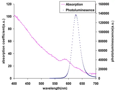
Figure 1 shows the absorption and photoluminescence spectra of CdSe/ZnS nanocrystals that we use in our scintillator with excitation wavelength at 325 nm and emission wavelength at 620 nm.
0 20 40 60 80 100 120 400 450 500 550 600 650 700 wavelength(nm) ab so rp ti on c o ef fi ci en t( a. u .) 0 20000 40000 60000 80000 100000 120000 140000 160000 ph ot ol u m in es cen ce (a .u .) Absorption Photoluminesence
Figure 1: The emission and absorption spectra of our CdSe/ZnS core-shell nanocrystals.
In the first set of experiments, we use nanocrystal films on quartz substrate integrated with the detector. We use CdSe/ZnS nanocrystals hosted in a polymer matrix. In operation, the incident light first hits the nanocrystal film, and subsequently the light emitted by the nanocrystals is collected by the detector underneath.
The excitation spectrum of the nanocrystal films is very important because it defines the efficiency of the scintillator as a function of the incident wavelength. Figure 3 shows the ratio of the emitted power to the incident power for different excitation wavelengths.
Here the optical characteristics of the host polymer play a critical role. The host polymer should exhibit low optical absorption in the ultraviolet spectral range of interest. Otherwise, the polymer matrix decreases the efficiency of the scintillator.
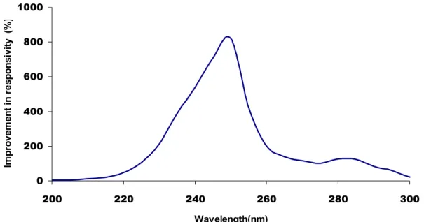
Figure 3 shows the enhancement of the power detected by the silicon detector in the ultraviolet range (between 200 nm and 320 nm) using CdSe/ZnS core -shell nanocrystals up to 800% with respect to the host polymer. This proof-of-concept experiment shows us that nanocrystal based scintillators hold great promise.
Proc. of SPIE Vol. 6393 63930D-2
There is room for further improvement of the responsivity by using a host material with less optical absorption, higher nanocrystal concentration, optimal film thickness and nanocrystals with optimal emission wavelength.
0 5 10 15 20 25 200 220 240 260 280 300 320 340 360 380 400 Wavelength (nm) P em it te d /P in ( % )
Figure 2: The excitation spectrum of 1.7 µm thick film of our CdSe/ZnS core-shell nanocrystals in a polymer matrix on quartz substrate.
Figure 3: Enhancement of the power detected by the silicon detector in the ultraviolet with respect to the host polymer. 0 200 400 600 800 1000 200 220 240 260 280 300 Wavelength(nm) Im pr ove m ent i n r espo n si vi ty ( % )
Proc. of SPIE Vol. 6393 63930D-3
In the second set of experiments, we integrate our nanocrystals directly on the silicon photodetector. We use the same materials as in the first experiments. We achieve the responsivity enhancements of the hybrid detection system as high as 1000% times in the ultraviolet range. This scintillator approach holds promise for enhanced UV imaging.
We also work on the development of CdSe nanocrystals based electro-optical modulators. One way of implementing a modulator using nano material is through electroabsorption. Due to the quantum confined stark effect, when electric field is applied, the absorption coefficient of the nanocrystals changes. If the nanocrystal size distribution is uniform, large changes in the absorption coefficient can be achieved. For example, Figure 4 displays the optical absorption change of close-packed CdSe nanocrystals as a function of the applied electric field derived from our Phoremost research partners in the work of Artemyev et al. [2]. The large dependence of the absorption coefficient on the electric field means that CdSe nanocrystals can be used for device application as an electroabsorption modulator.
0 2000 4000 6000 8000 10000 12000 30 40 50 60 70 80 90 100 110 F (V/ micrometer) ch ang e i n ab s. c o ef. (1/ cm)
Figure 4: Change in the absorption coefficient of close-packed CdSe nanocrystals as a function of the electric field.
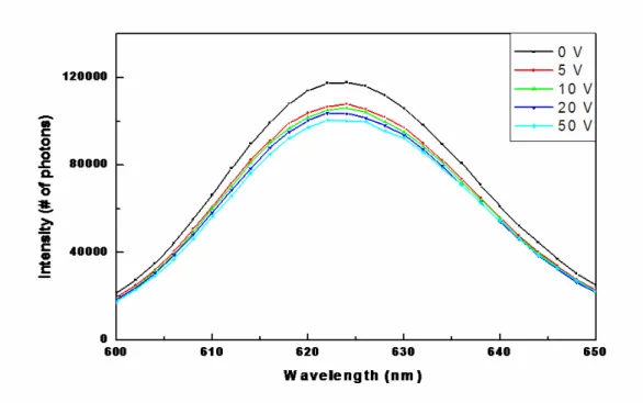
Another type of modulator that is possible using CdSe nanocrystals as the active material is a luminescence modulator. The photoluminescence efficiency of nanocrystals decreases under the influence of electric field. This has two basic reasons: the electric field causes electron-hole separation, and field-induced tunneling out of the quantum dot is expected under high electric field. Also, as a result of the electric field, the electron and the hole are attracted to the opposite sides of the material, which reduces the band gap, causing a red shift in the photoluminescence. Even though the red-shift is difficult to be used for modulating purposes, the reduction in the photoluminescence by removing the photogenerated carriers before they recombine is a potential way of modulating the optical signal by changing the electrical signal. Figure 5 shows the reduction of the photoluminescence of a film of CdSe nanocrystals with the effect of different potentials. Here the nanocrystals have a broad size distribution and the film is not thin enough; thus the photoluminescence change per unit field change is small under these non-optimal conditions.
Proc. of SPIE Vol. 6393 63930D-4
120000
a
C0
00000It
a
40000 0 600 610 620 630 640 Wavelength (nm)Figure 5: The change in photoluminescence of a film of CdSe nanocrystals as a function of applied bias.
3. TITANIUM DIOXIDE NANOPARTICLES
Another class of nanoparticles that have many different potential uses is the titanium dioxide nanoparticles. These nanoparticles exhibit photocatalytic behavior and can be integrated in devices and on surfaces for different self-cleaning applications such as environmental bio-decontamination for a large variety of organics, viruses, bacteria, fungi and cancer cells, chemical and biological purification of water, and prevention of air pollution by reducing NOx and COx
levels in air [7-13]. In these applications, the efficiency of the optical activation is critical because the decontamination process may require very long time or may be even impossible if the correct conditions are not satisfied, depending on the size and characteristics of the medium.
The performance of these photocatalytic nanoparticles depends on the process of optical absorption of photons and subsequent photogeneration of electron and hole pairs, which exhibit dissimilar parity in the respective conduction and valance bands. This causes low recombination rates, which is the key for superior photocatalytic characteristics. The long-lived photogenerated electron-hole pairs diffuse to the nanoparticle surface and initiate a chain of reactions to produce reactive oxygen species and hydroxyl radical that are powerful indiscriminate oxidizing agents. To initiate this process, the wavelength of the incident photon should be smaller than or equal to 385 nm as the band-gap of titanium dioxide nanoparticles is 3.2 eV (for anatase type).
To achieve high level of decontamination, it is necessary to optically activate the titanium dioxide nanoparticles efficiently. For this purpose, we study the behavior of their optical activation and understand its evolution in time. The behavior depends on a number of parameters including the size of the nanoparticles, the activation wavelength, and the number of photons used per area during the activation process.
In this work to understand the influence of these parameters, we optically investigate TiO2 nanoparticles of 6 nm and 21
nm sizes embedded in solgel films in the spectral range from 290 nm to 390 nm. Here for the first time we introduce the optical efficiency curves and the behavior of their optical activation in time as a function of activation wavelength and nanoparticle size in the near ultraviolet range.
Proc. of SPIE Vol. 6393 63930D-5
Figure 6 shows pictures of our sample that includes 6 nm, anatase-type TiO2 nanoparticles, embedded in a 10 µm thick
acrylic solgel film and contaminated with methylene blue solution. Figure 6 exhibits the self-cleaning effect within the spot size of the activating ultraviolet illumination at the center of the sample, in contrast to the non-activated region around the spot. We observe that the contaminated region is optically recovered back further towards its original as a result of the photocatalytic effect.
Figure 6: Sample photographs of 6 nm TiO2 nanoparticles in 10 µm thick acrylic solgel film (a) before
contamination, (b) after contamination with no UV activation, and (c) after contamination with UV activation. There is color change across the UV beam spot as a result of the photocatalytic process.
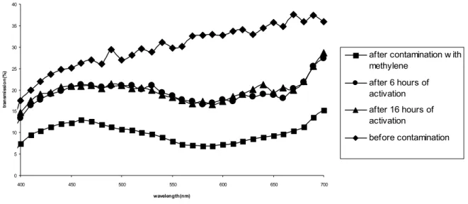
We investigate the efficiency of the photocatalytic process quantitatively. We conduct the first set of the experiments to study the effect of the nanoparticle size on the photocatalytic process. Figure 7 shows the optical transmission spectra of 21 nm TiO2 samples before and after the methylene blue contamination in the visible range from 400 nm to 700 nm,
along with the time evolution of the transmission spectra under UV activation with the optical power of 200 µW at 330 nm after 6 and 16 hours. Here the methylene blue contamination shifts the optical transmission curve to lower values significantly in the visible range. We observe that the optical transmission of the contaminated sample returns towards its initial values significantly back after the first 6 hours of photoexcitation process, but changes only slightly between the 6 hours of photoexcitation and 16 hours of photoexcitation. This is an indication of saturation of the photocatalytic process.
On the other hand, Figure 8 displays the optical transmission spectra of 6 nm TiO2 samples in the same spectral range at
the same time intervals under the same UV radiation conditions. In this experiment, we observe that the decontamination process of the 6 nm nanoparticles does not saturate after 6 hours of activation, unlike the 21 nm sample, but continues further to higher recovery levels. This is clearly evident in the optical transmission spectrum measured after 16 hours of photoexcitation in Figure 8. As we further continue the photoactivation, we obtain more than 90% photocatalytic recovery of the contamination after the first set of optical activation and even better after multiple sets of activation. This critical influence of size on the optical activity of photocatalytic process is due to the increased surface-to-volume ratio as the size gets smaller. This means that we can improve the effectiveness of TiO2 nanoparticles further by using
smaller nanoparticles.
The photocatalytic processes require photogenerated electron-hole pairs. Therefore, we compare the efficiencies of photocatalytic processes under different conditions as a function of the number of photons per unit area. For quantitative comparison, we calculate the optical efficiency from the optical transmission of the samples before and after contamination, and after decontamination with different activation wavelengths, durations, and different solutions for contamination.
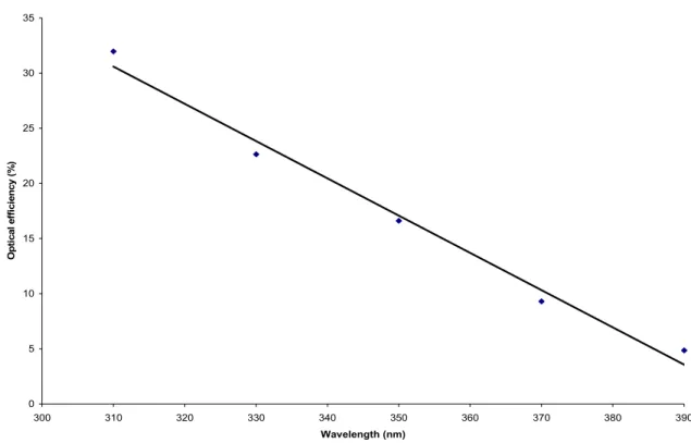
Figure 9 shows the optical efficiency in the initial phase of 6 nm nanoparticles as a function of the activation wavelength as a fixed number of photons per unit area. Here we calculate the optical efficiency curve by normalizing the area integrated between the optical transmission of the activated sample and the optical transmission of the contaminated sample in the visible range between 400 nm and 700 nm with respect to the area between the optical transmissions of the original and contaminated samples.
Proc. of SPIE Vol. 6393 63930D-6
0 5 10 15 20 25 30 35 40 400 450 500 550 600 650 700 wavelength(nm) tr an sm is si o n (%)
after contamination w ith methylene after 6 hours of activation after 16 hours of activation before contamination
Figure 7: Optical transmission of the solgel film that incorporates 21 nm size TiO2 nanoparticles before and after
the contamination with UV activation of 0-16 hours.
0 5 10 15 20 25 30 400 450 500 550 600 650 700 wavelength (nm) tr an sm is si o n ( % ) before contamination after contamination w ith methylene after 6 hours of activation after 16 hours of activation
Figure 8: Optical transmission of the solgel film that incorporates 6 nm size TiO2 nanoparticles before and after
the contamination with UV activation of 0-16 hours.
Proc. of SPIE Vol. 6393 63930D-7
0 5 10 15 20 25 30 35 300 310 320 330 340 350 360 370 380 390 Wavelength (nm) O p ti ca l ef fi ci en cy (% )
Figure 9: Optical efficiency curve of 6 nm nanoparticles for different activation wavelengths for activation with 10^23 photons / m^2. 0 10 20 30 40 50 60 70 80 90 100
5E+23 7E+23 9E+23 1.1E+24 1.3E+24 1.5E+24 1.7E+24 1.9E+24 2.1E+24 2.3E+24
Number of photons / area (1/m^2)
O p ti cal ef fi ci en cy( % )
Figure 10: Optical efficiency curve of 6 nm nanoparticles optically activated at 330 nm in the late phase of the decontamination process.
Proc. of SPIE Vol. 6393 63930D-8
Figure 10 shows the optical efficiency of 6 nm nanoparticles activated at 330 nm at the late phase of the photocatalytic process as a function of number of activation photons per unit area. This characterization shows that more than 90 % decontamination can be achieved if suitable nanoparticles and suitable activation wavelengths are selected. Using multiple sets of activation, even higher levels of decontamination can be obtained.
In this work on titanium dioxide nanoparticles, we characterize the optical activation curves of 6 nm and 21 nm TiO2
nanoparticles embedded in solgel under different activation conditions. We quantitatively compare the activation efficiencies for different wavelengths and numbers of photons. We prove that smaller nanoparticles have significantly higher optical efficiencies than the larger ones under identical activation conditions.
4. CONCLUSIONS
We work on different applications of nanoparticles in optoelectronic and optical devices within our EU FP7 Phoremost Network of Excellence on nanophotonics. One type of these nanoparticles is CdSe/ZnS core-shell nanocrystals. These nanocrystals can be functionally used as scintillators and modulators with the proper selection of material and proper design. We show that the nanocrystal based scintillators improve the UV detection significantly on a silicon platform. Also, thanks to the quantum confined stark effect, we can use the strong dependence of absorption and emission characteristics of nanocrystals in electro-optical modulators.
We also work on the applications of titanium dioxide nanoparticles for photocatalytic processes in collaboration with DYO. For the first time we obtain optical efficiency curves of these nanoparticles during the decontamination process. Using these efficiency curves, we show that smaller titaniumdioxide nanoparticles are better self-cleaners.
Acknowledgements - This work is supported by EU MOON, EU NOE PHOREMOST and TUBITAK 104E114,
106E020, 105E065, and 105E066. H.V.D and I.M.S. also acknowledge support from Turkish Academy of Sciences and TUBITAK, respectively.
REFERENCES
1. B. O. Dabbousi, J. R. Viejo, F. V. Mikulec, J. R. Heine, H. Mattoussi, R. Ober, K. F. Jensen, and M. G. Bawendi, “(CdSe)ZnS core-shell quantum dots: synthesis and characterization of a size series of highly luminescent nanocrystallites”, J. Phys. Chem. B, 101, 9463-9475, 1997.
2. M. V. Artemyev, U. Woogon, H. Jaschinski, L. I. Gurinovich, S. V. Gaponenko, “Spectroscopic study of electronic states in an ensemble of close-packed CdSe nanocrystals”, J. Phys. Chem. B., 104, 11617-11621, 2000.
3. J. Seufert, M. Obert, M. Scheibner, N. A. Gippius, G. Bacher, A. Forchel, T. Passow, K. Leonardi, and D. Hommel, “Stark effect and polarizability in a single CdSe/ZnSe quantum dot”, Applied Physics Letters, vol. 79, no. 7, pp. 1033-1035, 2001.
4. S. A. Empedocles, D. J. Norris, and M. G. Bawendi, “Photoluminescence spectroscopy of single CdSe nanocrystallite quantum dots”, Phys. Rev. Lett., 77, 18, 1996.
5. C. A. Leatherdale, W. K. Woo, F. V. Mikulec, and M. G. Bawendi, “On the absorption cross section of CdSe nanocrystal quantum dots”, J. Phys. Chem. B, 106, 7619, 2002.
6. S. Banerjee, J. Gopal, P. Muraleedharan, A. K. Tyagi, and B. Raj, “Physics and chemistry of photocatalytic titanium dioxide: visualization of bactericidal activity using atomic force microscopy”, Current Science, 90, 1378, 2006.
7. N. Savage, M. S. Diallo, “Nanomaterials and water purification: opportunities and challenges”, Journal of Nanoparticle Research, 7, 331, 2005.
8. N. S. Allen, M. Edge, G. Sandoval, J. Verran, J. Stratton, and J. Maltby, “Photocatalytic coatings for environmental applications”, Photochemistry and Photobiology, vol. 81, no.2, pp. 279, 2004.
Proc. of SPIE Vol. 6393 63930D-9
9. R. Ota et al., Proc. of 5th International Workshop on Photocatalytic Systems, EJIPAC, 37, 2005.
10. S. Ishikawa et al., Proc. of 5th International Workshop on Photocatalytic Systems, EJIPAC, 42, 2005.
11. X. Zili, J. Shang, C. Liu, C. Kang, H. Guo, Y. Du, “The preparation and characterization of TiO2 ultrafine particles”,
Materials Science and Engineering. B56, pp. 211-214, 1999.
12. J. Liqiang, S. Xiaojun, C. Weimin, X. Zili, D. Yaoguo, F. Honggang, “The preparation and characterization of nanoparticle TiO2/Ti films and their photocatalytic activity ”, Journal of Physics and Chemistry of Solids 64, pp.
615-623, 2003.
Proc. of SPIE Vol. 6393 63930D-10