PROCEEDINGS OF SPIE
SPIEDigitalLibrary.org/conference-proceedings-of-spiePhysics and applications of defect
structures in photonic crystals
Ekmel Ozbay
Kaan Guven
Physics and Applications of Defect Structures in Photonic Crystals
Ekmel Ozbay, Kaan Guven, and Mehmet Bayindir
Department of Physics, Bilkent University, Ankara, Turkey, 06533
ABSTRACTPhotonic crystals are three dimensional periodic structures having the property of reflecting the electromagnetic (EM) waves in all dimensions, for a certain range of frequencies. Defects or cavities around the same geometry can also be built by means of adding or removing material. The electrical fields in such cavities are usually enhanced, and by placing active devices in such cavities, one can make the device benefit from the wavelength selectivity and the large enhancement of the resonant EM field within the cavity. By using coupled periodic defects, we have experimentally observed a new type of waveguiding in a photonic crystal. A complete transmission was achieved throughout the entire waveguiding band. The transmission, phase, and delay time characteristics of the various coupled-cavity structures were measured and calculated. We observed the eigenmode splitting, waveguiding through the coupled cavities, splitting and switching of electromagnetic waves in waveguide ports, and Mach-Zender interferometer effect in such structures. The corresponding field patterns and the transmission spectra were obtained from the finite-difference-time-domain (FDTD) simulations. We developed a theory based on the classical wave analog of the tight-binding (TB) approximation in solid state physics. Experimental results are in good agreement with the FDTD simulations and predictions of the TB approximation.
Keywords: Photonic Crystals, Coupled Cavity, Waveguide, FDTD, Mach-Zehnder, Tight Binding Approximation.
1. INTRODUCTION
Photonic crystals are artificial dielectric or metallic structures in which the refractive index modulation gives rise to stop bands for electromagnetic waves within a certain frequency range in all directions.1,2 Recognized as an effective tool to control of the propagation of EM wave, photonic crystal based structures rapidly attracted a great interest in recent years and are envisaged as the main candidate to develop into next generation lightwave circuits. Current research activities concerning photonic crystals involve many scientific and engineering applications such as, localization of photons,3 lasers,4,5,6 waveguides,7,8,9,10,11 splitters,12,13,14 fibers,15 antennas,16,17 optical circuits,18,19 and ultra fast optical switches.20
The analogy between the Schrödinger Equation for an electron moving in a periodic crystal potential and the Maxwell’s equations for an EM wave propagating through a medium with periodically modulated refractive index allows many important models and formulations originally to be applied to the photonic crystals which were originally developed for electronic solid state systems. In particular, by introducing “defects” to a photonic crystal, which can be realized by adding or removing materials, it is possible to create localized EM modes inside the photonic band-gap which are reminiscent of the acceptor and donor impurity states in a semiconductor.21,22 Consequently, photons with certain wavelengths can locally be trapped inside the defect volume. This important property can be used in various photonic applications. In fact, most of the aforementioned applications are based on cavity structures built in photonic crystals.
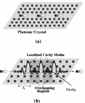
The guiding of EM waves in photonic crystals is obtained either along a line defect (a row of missing rods)8,11 or through coupled cavities.10 In the former case, while the EM waves are confined in one direction which is perpendicular to the axis of missing rods, and photons can propagate in other directions parallel to the axis of the missing rods [Fig. 1(a)]. In the case of the coupled cavity waveguides (CCWs), the EM waves are tightly confined at each defect side, and photons can propagate by hopping, due to interactions between the neighboring evanescent cavities modes [Fig. 1b].
Fig. 1 Schematic drawing of two different waveguiding mechanisms in photonic crystals. (a) Planar waveguides (PW) consist of two parallel photonic crystal mirrors with a suitable separation between them. Photons confined between these two photonic crystal walls, and can propagate through the opening which can be considered a continuous defect. (b) Coupled-cavity waveguides (CCWs) are formed by removing an array of rods (white circles) from a two-dimensional photonic crystal (black circles). Tightly confined cavity mode interacts weakly with the neighboring cavity modes, and therefore the electromagnetic waves can propagate through
coupled cavities.
Recent studies indicate that the photonic coupled-cavity waveguide based structures may alleviate many problems concerning the current waveguide applications. Shape independent 100% throughput, wider range to control the group velocity and photon lifetime, efficient channel add-drop filters,21,22,23 and wave-guide networks with vanishing cross talk24,25 are few to name among these properties.
This paper is organized as follows: In section 2, the localized cavity-modes in two-dimensional photonic band gap structures are investigated in detail. The splitting of the eigenmode of a cavity is obtained for two coupled cavity case. Transmission spectra, field distributions and photon delay times of experiments and of finite-difference-time-domain (FDTD) simulations are presented along with the predictions of the Tight Binding (TB) approximation. In section 3, several application possibilities of the CCWs are demonstrated experimentally and by corresponding FDTD simulations.
2. LOCALIZATION OF THE ELECTROMAGNETIC FIELD BY MEANS OF CAVITIES IN
PHOTONIC CRYSTALS 2.1 Localized Coupled-Cavity Modes and the Tight Binding Approximation
It is well known that the tight binding (TB) method has proven to be very useful in studying the electronic properties of solids.26 Recently, the classical wave analog of the tight binding (TB) model27,28 has successfully been applied to photonic structures.29,30,31,32,33,34 By using direct implications of the TB picture, a novel propagation mechanism for photons along localized coupled cavity modes in photonic crystals was theoretically proposed30,33 and experimentally demonstrated.34 In these structures, photons can hop from one tightly confined mode to the neighboring one due to weak interaction between them [see Fig. 1(b)]. Stefanou and Modinos obtained the cosine-like dispersion relation for their coupled-defect waveguide and waveguide bends with and without disorder.30 Yariv et al. reformulated the same phenomenon in a simple way, and proposed various applications based on coupled-cavity structures.33 Later,
the mode splitting phenomena within the TB picture,34 guiding and bending of EM wave,10 heavy photons,35 and EM-beam splitting and switching effect47 were experimentally demonstrated in our group in three-dimensional photonic crystals at microwave frequencies. Very recently, Lan et al. numerically proposed a switching mechanism by changing the positions of the sharp edges of the coupled-cavity band of 1D PBG structures36 and delay lines for ultra short optical pulses37, and Olivier et al. reported 2D CCWs at optical wavelengths.38
This section presents shortly the theoretical formulation for the splitting of the eigenmode of a cavity when coupled with one or two cavities, using the TB approach. This can be extended to the n coupled cavities, i.e. the coupled-cavity waveguide. Simple expressions for dispersion relation, group velocity and photon lifetime are derived.
A cavity formed within a photonic band gap material supports a strongly localized mode
E
r
Ω(r
r
)
, which satisfies the Maxwell equation:[
r
E
r
(
r
r
)
]
0(
r
r
)(
/
c
)
2E
r
(
r
r
),
r
Ω Ω=
Ω
×
∇
×
∇
ε
1where
ε
0(
r
r
)
is the dielectric constant of the single cavity and Ω is the frequency of the corresponding cavity mode. Here, it is assumed thatE
r
Ω(r
r
)
is real, nondegenerate and orthonormal.When two cavities are placed close to each other, the corresponding eigenmode can be obtained from the superposition of the individual evanescent cavity modes
E
r
ω(
r
r
)
=
A
E
r
Ω(
r
r
)
+
B
E
r
Ω(
r
r
−
Λ
x
ˆ
)
. The eigenmodeE
r
ω(r
r
)
also satisfies (1) whereε
0(
r
r
)
is replaced with the dielectric constant of the coupled systemε
(
r
r
)
=
ε
(
r
r
−
Λ
x
ˆ
)
, and Ω is replaced with eigenfrequency ω of the coupled cavity mode. InsertingE
r
ω(r
r
)
into (1), and multiplying both sides from the left first byE
r
Ω(r
r
)
, and then byE
r
Ω(
r
r
−
Λ
x
ˆ
)
and spatially integrating the resulting equations, we obtain the following eigenmodes and eigenfrequencies:2
)
ˆ
(
)
(
)
(
2 , 1x
r
E
r
E
r
E
=
Ω±
Ω−
Λ
r
r
r
r
r
r
ω 2 1 1 2 , 11
1
α
β
ω
±
±
Ω
=
3where α1 and β1 are the first order coupling parameters which are given by 1
=
∫
d
r
(
r
)
E
Ω(
r
)
⋅
E
Ω(
r
−
Λ
x
ˆ
)
r
r
r
r
r
r
ε
α
, and∫
−
Λ
⋅
−
Λ
=
0(
ˆ
)
Ω(
)
Ω(
ˆ
)
1d
r
r
x
E
r
E
r
x
r
r
r
r
r
ε
β
.The eigenmodes of three coupled cavities can be obtained similarly. In this case, introducing second nearest neighbor coupling terms
α
2=
∫
d
r
r
ε
(
r
r
)
E
r
Ω(
r
r
)
⋅
E
r
Ω(
r
r
−
2
Λ
x
ˆ
)
, andβ
2=
∫
d
r
r
ε
0(
r
r
−
2
Λ
x
ˆ
)
E
r
Ω(
r
r
)
⋅
E
r
Ω(
r
r
−
2
Λ
x
ˆ
)
one gets the eigenmodes and eigenfrequencies as follows:2
)
ˆ
2
(
)
(
)
(
2
)
ˆ
2
(
)
ˆ
(
2
)
(
)
(
2 3 , 1x
r
E
r
E
r
E
x
r
E
x
r
E
r
E
r
E
Λ
−
−
=
Λ
−
+
Λ
−
±
=
Ω Ω Γ Ω Ω Ω Γr
r
r
r
r
r
r
r
r
r
r
r
r
r
, 42 2 2 2 1 2 1 3 , 1
1
1
2
/
2
1
2
/
2
1
α
β
α
α
β
β
−
−
Ω
=
Γ
+
±
+
±
Ω
=
Γ
. 5For an array of cavities, where each cavity interacts weakly with neighboring cavities, a defect band (waveguiding band) is formed. Similar to the two coupled cavity case, the eigenmode of this waveguiding band can be written as a superposition of the individual cavity modes. For n cavities one would write
∑
−
Λ
=
− Λ Ω n inkx
n
r
E
e
E
r
E
r
(
r
)
0r
(
r
ˆ
)
6A simple expression for the dispersion relation of the waveguiding band can be obtained from (1) and (7), keeping only the nearest neighbor coupling terms
[
1
cos(
)
]
)
(
k
=
Ω
+
κ
k
Λ
ω
, 7where
κ
=
β
1−
α
1is a Tight Binding parameter which can be obtained from the splitting of the eigenmodes of two coupled cavities. After obtaining Ω, ω1, and ω2 from measurements or simulations, one can determine α1, and β1 values by using (3). The bandwidth of the waveguide is proportional to the coupling constant and to the single cavityfrequency:
Ω
=
∆
ω
2
κ
. 8The group velocity of photons along the waveguide ca be determined from the dispersion relation
)
sin(
)
(
k
=
∇
=
−
ΛΩ
k
Λ
v
g kω
kκ
. 9The additional phase acquired by an EM wave propagating through the photonic crystal of thickness L is
L
k
kL
−
0=
∆ϕ
, wherek
0=
2
πω
/
c
is the wave vector in vacuum, and c is the speed of light in vacuum. The delay time (photon lifetime) is defined asω
ϕ
τ
p=
∂
(
∆
)
/
∂
. 10Using the expression for the phase difference and (5), delay time can be written as a function of frequency
c
L
L
p2
/
)
1
/
(
/
)
(
2 2ω
π
κ
ω
τ
−
−
Ω
−
Ω
Λ
=
. 11An immediate indication of this formula is that at the delay time increases rapidly at the edges of the waveguiding band. This behavior can be utilized for applications which require low group velocity and long photon lifetimes.
The TB formulation implies that relevant physical quantities such as the dispersion relation and group velocity depend only on a single TB parameter κ, which can be controlled by changing the cavities and the intercavity distance. Thus, having κ as a design parameter, one can construct coupled cavity structures for certain applications such as dispersion compensators and photonic switches.
2.2 Coupled Cavity Structures: Experiments and Theoretical Calculations
We first constructed 2D triangular photonic crystals which consist of dielectric cylindrical alumina rods having radius 1.55 mm and refractive index 3.1 at the microwave frequencies. The lattice constant and the corresponding filling fraction are a = 1.3 cm and η ~ 0.05, respectively. Length of the rods is 15 cm. The experimental set-up consisted of a HP 8510C network analyzer and microwave horn antennas to measure the amplitude and the
transmission-phase properties. The transverse magnetic (TM) polarization, the incident electric field was parallel to the rods, is considered in all measurements. It is well known that the other polarization, transverse electric (TE), does not produce any photonic band gaps in this frequency range.1 In experiments, the transmission and phase spectrum in the absence of photonic crystal (i.e. free space) is measured and this data is used as the calibration data of the network analyzer. Then, the crystal is placed between the horn antennas, and the transmission and phase measurements are performed. The distance between transmitter and receiver antennas is kept constant throughout the calibration and measurement phases. The transmission spectra and the field patterns are then obtained by using FullWave which is a commercially available finite-difference-time-domain (FDTD) code. In FDTD simulations, the transmission spectrum was normalized with respect to the source spectra.
Figure 2: [Left panels] Measured (solid lines) and calculated (dotted lines) transmission spectra for (a) a single cavity, (b) two coupled cavity, and (c) three coupled cavity structures. Due to coupling between the strongly localized cavity modes, single cavity
mode splits into two or three distinct modes depending on the number of coupled cavities. [Right panels] Schematics of the corresponding coupled-cavity structures where white circles denote the removed rods.
The crystal exhibits a photonic band gap extending from 0.73ω0 to 1.14ω0 where ω0 = c/2a = 11.54 GHz. Figure 2 shows the measured and calculated transmission characteristics of various coupled-cavity structures along with the schematic drawing of these structures. When a single rod is removed from otherwise perfect crystal, a highly localized cavity mode appears at frequency Ω0 = 0.908 ω0 having a quality factor of 900 [Fig. 2(a)]. The transmission through a crystal which contains two coupled cavities with an intercavity distance Λ=√3a is shown in Fig. 2(b). Here, the splitting of the single cavity mode into two resonance modes at ω1 = 0.879 Ω0 and ω2 = 0.928 Ω0 is observed.
Localized defect modes in 2D photonic crystals are widely studied in literature,39,40,41 and splitting of the eigenmode is already reported for various photonic structures. This phenomenon is observed in 3D diamond wire mesh photonic crystals,42 coupled dielectric spheres,43,44 coupled pairs of micrometer-sized semiconductor cavities,45 polymer bispheres in contact,32 and coupled defects in 3D dielectric photonic crystals.34
In the case of three coupled cavities, the eigenmode splits into three resonance frequencies. As shown in Fig. 2(c), there is a good agreement between measured and simulated results. We also compare the TB predictions of the resonant frequencies Γ1,2,3 with the measured and the FDTD simulation results (see Table 1).
Measurement FDTD TB TB† Γ1 0.869 0.871 0.863 0.866 Γ2 0.904 0.903 0.908 0.904 Γ3 0.938 0.940 0.935 0.937
Table 1. Comparison of the resonant frequencies of three coupled cavities obtained by measurements, by the FDTD simulations, and by the TB approximation. (†Second nearest neighbor coupling included)
The measured delay time as a function of frequency in these coupled-cavity structures is shown in Fig. 3. The strong enhancement of the delay time indicates that the incident EM field with the coupled cavity resonance frequencies becomes confined within the cavities and propagate more slowly compared to free space propagation.
Figure 3: Measured delay time characteristics of the (a) single cavity, (b) two coupled-cavities, (c) three coupled-cavities, respectively. τp exhibits peaks at the resonance frequencies of the corresponding coupled-cavity structures.
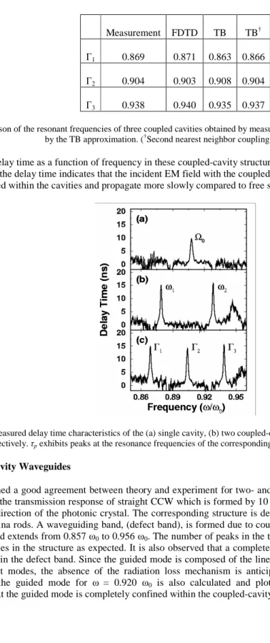
2.3 Coupled-Cavity Waveguides
Having established a good agreement between theory and experiment for two- and three coupled-cavity structures, we now investigate the transmission response of straight CCW which is formed by 10 consecutive defects, along a straight line in the ΓM direction of the photonic crystal. The corresponding structure is depicted in Fig 4(b). The small circles denote the alumina rods. A waveguiding band, (defect band), is formed due to coupling between the evanescent defect modes. This band extends from 0.857 ω0 to 0.956 ω0. The number of peaks in the transmission spectrum is equal to the number of cavities in the structure as expected. It is also observed that a complete transmission is achieved for certain frequencies within the defect band. Since the guided mode is composed of the linear combination of strongly localized individual defect modes, the absence of the radiation loss mechanism is anticipated in these structures. The field distribution of the guided mode for ω = 0.920 ω0 is also calculated and plotted on Fig. 4 (right panel) which demonstrates that the guided mode is completely confined within the coupled-cavity array and propagated through it.
Figure 4: (a) Measured (solid line) and calculated (dotted line) transmission spectra of the straight coupled-cavity waveguide which is generated by removing 10 adjacent rods from the crystal. The waveguiding band extends from 0.857 ω0 to 0.956 ω0. Nearly 100
percent transmission is achieved for certain frequencies. (b) Calculated field distribution of the CCW for a frequency within the cavity band, namely, ω=0.920 ω0. The guided mode is localized in and travels along the cavities. The electric field is polarized along
the axis of the (missing) rods.
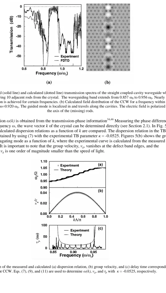
The dispersion relation ω(k) is obtained from the transmission-phase information34,46 Measuring the phase difference ∆φ as a function of frequency ω, the wave vector k of the crystal can be determined directly (see Section 2.1). In Fig. 5(a), the measured and calculated dispersion relations as a function of k are compared. The dispersion relation in the TB approximation is obtained by using (7) with the experimental TB parameter κ = -0.0525. Figures 5(b) shows the group velocity of the propagating mode as a function of k, where the experimental curve is calculated from the measured dispersion relation. It is important to note that the group velocity, vg, vanishes at the defect band edges, and the
maximum value of vg is one order of magnitude smaller than the speed of light.
Figure 5: Comparison of the measured and calculated (a) dispersion relation, (b) group velocity, and (c) delay time corresponding to the straight CCW. Eqs. (7), (9), and (11) are used to determine ω(k), vg, and τp with κ = -0.0525, respectively.
The measured (solid line) and calculated (dotted line) delay time characteristics are displayed in Fig. 5(c). The delay time increases drastically at the band edges, which supports the behavior obtained by the TB analysis (11). One can also draw an analogy to the heavy electron in semiconductors, which has energy near the band edge,28 and describe the photons having energies close to the waveguide band edges as heavy photons.
3. APPLICATIONS OF COUPLED-CAVITY WAVEGUIDES (CCWs) IN PHOTONIC
CRYSTALS 3.1 Splitters and Switches
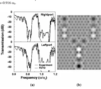
Splitters and switches are important components for designing photonic circuits. In recent years, many authors reported splitters and switches which are built around photonic band gap structures.12,13,14,47 In this section, we demonstrate splitting of propagating waves into to two output waveguide ports. We also report a switching mechanism based on coupled-cavity structures.
In order to demonstrate the splitting of EM power, we construct a Y-shaped splitter which consists of one input CCW and two output CCWs. The input and output waveguide ports contain 5 and 6 coupled cavities, respectively. As shown in Fig. 6 (left panel), the propagating mode inside the input CCW splits equally into two output CCW ports for all frequencies within the defect band. We also compute the electric field distribution inside the input and the output CCW channels for frequency ω=0.916 ω0.
Figure 6: (a) Measured (solid line) and calculated (dotted line) of transmission spectra of a Y-shaped coupled-cavity based splitter. The electromagnetic power in the input port splits equally into the two output waveguide ports for frequencies throughout the cavity
band. (b)The calculated power distribution inside the input and the output channels of the splitter for frequency ω=0.916 ω0
The present structure can also be used as a photonic switch. To demonstrate the switching effect, we place a single rod to the left side of junction of Y-splitter. This breaks the symmetry of the structure, and therefore one can regulate the amount of power flow into the output ports of CCWs. As shown in Fig. 7, the power at each output waveguide port is drastically changed. While most of the input power for frequencies throughout the defect band is coupled to the right port, only a few percent of the input power is coupled to the left port. The simulated electric field distribution is also displayed in right panel of Fig 7.
Figure 7: (a) Measured (solid line) and calculated (dotted line) transmission characteristics of a coupled-cavity switching structure. (b) Corresponding field pattern clearly indicates that most of the power is coupled to the right port.
3.2 Mach-Zehnder Interferometer employingCCWs
Mach-Zehnder interferometers have been widely implemented in optical devices such as demultiplexers, switches and intensity modulators.48 The size of these structures is an important issue for large-scale optical integration. Current all-optical and electro-all-optical switches are of the order of millimeters, and carry little potential for further size reduction. Operation of active optic elements is based on the change of the index of refraction induced by electro-optical or nonlinear optical effects. However, the changes that can be achieved are very small (δn ~ 0.001), and inducing a shift to the phase of the signal by π typically requires propagation lengths of the order of millimeter. The same length considerations apply to phase shifts induced solely by path differences. From this point of view, the coupled cavity waveguides are very promising candidates for developing compact optical devices, because the group velocity of the propagating EM wave can be reduced drastically. The reduction of the group velocity provides both the enhancement of the nonlinear effects, and the increase of the effective length of the waveguide compared to its geometrical length. Very recently, both these benefits are investigated on Mach-Zehnder interferometer structures based on photonic crystal CCWs.49,50
In this section, a Mach-Zehnder interferometer structure based on photonic crystal CCWs is demonstrated experimentally and by FDTD simulations. For this purpose, cylindrical alumina rods of radius 0.155 mm are assembled to a two-dimensional cubic lattice of period 1.1 cm. The structure exhibits a photonic band gap extending from 9.016 GHz to 13.153 GHz. The Mach-Zehnder interferometer is constructed by two CCW branches, consisting of 10 cavities (long branch) and 8 cavities (short branch), respectively. The operation principle is based on the difference of the cavity number [see Ref. 50]. The intercavity spacing is twice the lattice period. The input and output ports are also CCWs having identical cavity characteristics as the MZI branches. Figure 8 shows the schematic top view of the simulation structure built according to the experimental parameters.
Figure 8: Normalized and grayscale coded index profile of the simulated MZI structure which is constructed using experimental setup parameters. Dark circles correspond to the cylindrical alumina rods (highest index of refraction). The branches consist of
CCWs with 10 and 8 cavities, respectively. The input and output waveguides are also CCWs consisting of 3 cavities.
In order to show that no significant bending losses are present despite the sharp corners of the CCWs in the MZI, we measured the transmission spectra of the long branch and the short branch of MZI separately (i.e. when the other branch is not present), and then compared the results with the transmission spectrum of a straight CCW. Figure 9 shows that all three CCWs support a guiding band ranging roughly between 10.8 – 12.1 GHz, with very similar transmission characteristics. Note that due to the difference in the number of cavities, the widths of the guiding band differ slightly.
Figure 9: Comparison of the transmission spectra for straight CCW (solid line), long branch of MZI (dash-dotted line) and short branch of MZI (dotted line).
Martinez et. al. have shown50 that the transfer function of the CCW based Mach-Zehnder Interferometer can be written as T11(f)=cos
2
(∆Lβ/2) where ∆L=∆Nd is the length difference written in terms of the difference in number of cavities of the branches, ∆N and β is the intrinsic propagation constant depending on the eigenfrequency of an isolated cavity, and on the intercavity coupling strength. d denotes the intercavity distance. Due to the periodicity of the CCW, β can take values in the reduced Brillouin zone as 0≤β≤π/d. This form of the transfer function suggests that ∆N/2 dips appear in the MZI output due to the destructive interference between different paths. The present MZI structure is configured for
∆N=2 and is expected to exhibit a single dip within the waveguiding band. Figures 10(a) and 10(b) show the
transmission response measured experimentally. We note that the structure was not optimized for maximum flatness in the guiding band. However, the comparison of the MZI transmission and the transmission of one of the branches shows that there is a strong dip located within the guiding band, which is found to be at 11.439 GHz.
Figure 10: (a) Experimental Transmission response of the MZI (solid line) and one of the CCW branches (dotted line). (b) Same as (a) but zoomed in to the guiding band region. (c) Comparison of the experimental measurement (solid line) and the FDTD simulation
calculation (dotted line) of the transmission response of the MZI. (d) Same as (c) but zoomed in to the guiding band region.
The transmission spectrum is then calculated from FDTD simulations performed with experimental parameters. Figures 10(c) and 10(d) compare the calculated transmission spectrum with experimentally measured spectrum showing both an overall good agreement, and a good match for the position of the dip.
Figure 11: The distribution of the incident EM field with frequency 11.439 GHz, inside the MZI. Left branch consists of 10 coupled cavities, and the right branch consists of 8 coupled cavities. The split field interferes destructively at the joint of two branches near
To see how the field distribution looks like when the MZI is in “off” state, a pulse having a frequency equal to the dip frequency is sent through the input port and the field distribution is calculated by FDTD method. Figure 11 shows that the field propagates through the branches of MZI, and interferes destructively at the cavity where the two branches join. Hence, no signal is present at the output port.
4. CONCLUSION
In this work, we presented a study of the coupled cavity structures in two-dimensional dielectric photonic crystals, and discussed some application possibilities. The splitting of the eigenmode of a cavity in the presence of coupling between the cavities is observed experimentally. An analysis within the Tight Binding formalism is performed on the structures having two-coupled cavities, three-coupled cavities, which gave the coupling parameter for these structures in very good agreement with the measurements. A comprehensive analysis of the coupled-cavity waveguide is carried out. The dispersion group velocity, photon delay times are measured and calculated as a function of frequency of the localized coupled-cavity mode. On the theoretical side, FDTD simulations were also performed which gave transmission characteristics in agreement with the measurements, and TB model’s predictions.
In photonic crystal based CCWs, the lossless transmission characteristics irrespective of the shape of the CCWs, and the extremely slow group velocity of the coupled modes close to the guiding band edges are emphasized. The latter is particularly important for applications demanding enhanced nonlinear effects, or having size restrictions. Among the many application possibilities of CCWs, simple splitter and switch structures are demonstrated experimentally, and by FDTD simulations. The slow group velocity of the coupled cavity modes further enables one to construct interferometer structures which produce large phase differences in considerably smaller sizes. This concept is elucidated by constructing a Mach-Zehnder interferometer which supports a mode within the waveguiding band, corresponding to a phase shift by π between the CCW branches.
1
J. D. Joannopoulos, R. D. Meade, and J. N. Winn, Photonic Crystals: Molding the Flow of Light, Princeton University Press, Princeton, NJ, 1995
2
For a recent review see articles in Photonic Crystals and Light Localization in the 21st Century, edited by C. M Soukoulis, Kluwer, Dortrecht, 2001.
3
S. John, “Strong localization of photons in certain disordered dielectric superlattices”, Phys. Rev. Lett. 58, pp. 2486-2489, 1987.
4
O. Painter, R. K. Lee, A. Scherer, A. Yariv, J. D. O'Brien, P. D. Dapkus, and I. Kim, “Two-dimensional photonic band-gap defect mode laser”, Science 284, pp. 1819-1821, 1999.
5
A. Mekis, M. Meier, A. Dodabalapur, R.E. Slusher, and J.D. Joannopoulos, “Lasing mechanism in two-dimensional photonic crystal lasers”, Appl. Phys. A: Materials Science & Processing 69, pp. 111-114, 1999.
6
S. Noda, M. Yokoyama, M. Imada, A. Chutinan, and M. Mochizuki, “Polarization mode control of two-dimensional photonic crystal laser by unit cell structure design”, Science 293, pp. 1123-1125, 2001.
7
A. Mekis, J. C. Chen, I. Kurland, S. Fan, P. R. Villeneuve, and J. D. Joannopoulos, “High transmission through sharp bends in photonic crystal waveguides”, Phys. Rev. Lett. 77, pp. 3787-3790, 1996.
8
Shawn-Yu Lin, E. Chow, V. Hietala, P. R. Villeneuve, and J. D. Joannopoulos, “Experimental demonstration of guiding and bending of electromagnetic waves in a photonic crystal”, Science 282, pp. 274-276, 1998.
9
B. Temelkuran and E. Ozbay, “Experimental demonstration of photonic crystal based waveguides”, Appl. Phys. Lett. 74, pp. 486-488, 1999.
10
M. Bayindir, B. Temelkuran, and E. Ozbay, “Propagation of photons by hopping: A waveguiding mechanism through localized coupled-cavities in three-dimensional photonic crystals”, Phys. Rev. B 61, pp. R11855-R11858, 2000. 11
M. Loncar, D. Nedeljkovic, T. Doll, J. Vuckovic, A. Scherer, and T. P. Pearsall, “Waveguiding in planar photonic crystals”, Appl. Phys. Lett. 77, pp. 1937-1939, 2000.
12
J. Yonekura, M. Ikeda, and T. Baba, “Analysis of finite 2-d photonic crystals of columns and lightwave devices using the scattering matrix method”, J. Lightwave Technol. 17, pp. 1500-1508, 1999.
13
R. W. Ziolkowski and M. Tanaka, “FDTD analysis of PBG waveguides, power splitters and switches”, Opt. Quant. Electron. 31, pp. 843-855, 1999.
14
T. Sondergaard and K. H. Dridi, “Energy flow in photonic crystal waveguides”, Phys. Rev. B 61, pp. 15688-15696, 2000.
15
J. C. Knight, J. Broeng, T. A. Birks, and P. St. J. Russell, “Photonic band gap guidance in optical fibers”, Science 282, pp. 1476-1479, 1998.
16
E. R. Brown, C. D. Parker, and E. Yablonovitch, “Radiation properties of a planar antenna on a photonic-crystal substrate”, J. Opt. Soc. Am. B 10, pp. 404-407, 1993.
17
B. Temelkuran, M. Bayindir, E. Ozbay, R. Biswas, M. M. Sigalas, G. Tuttle, and K. M. Ho, “Photonic crystal based resonant antenna with a very high directivity”, J. Appl. Phys. 87, pp. 603-605, 2000.
18
H. Kosaka, T. Kawashima, A. Tomita, M. Notomi, T. Tamamura, T. Sato, and S. Kawakamib, “Photonic crystals for micro lightwave circuits using wavelength-dependent angular beam steering”, Appl. Phys. Lett. 74, pp. 1370-1372, 1999.
19
A. de Lustrac, F. Gadot, S. Cabaret, J.-M. Lourtioz, T. Brillat, A. Priou, and A. E. Akmansoy, “Experimental demonstration of electrically controllable photonic crystals at centimeter wavelengths”, Appl. Phys. Lett. 75, pp. 1625-1627, 1999.
20
P. R. Villeneuve, D. S. Abrams, S. Fan, and J. D. Joannopoulos, “Single-mode waveguide microcavity for fast optical switching”, Opt. Lett. 21, pp. 2017-2019, 1996.
21
S. Fan, P. R. Villeneuve, J. D. Joannopoulos, and H. A. Haus, “Channel drop tunneling through localized states”, Phys. Rev. Lett. 80, pp. 960-963, 1998.
22
M. Bayindir and E. Ozbay, “Dropping of electromagnetic waves through localized modes in three-dimensional photonic band gap structures”, Appl. Phys. Lett. 81, pp. 4514-4516, 2002.
23
M. Bayindir and E. Ozbay, “Band dropping via coupled photonic crystal waveguides”, Opt. Exp. 10, pp. 1279-1284, 2002.
24
S. G. Johnson, C. Manolatou, S. Fan, P. R. Villeneuve, J. D. Joannopoulos, and H. A. Haus, “Elimination of cross talk in waveguide intersections”, Opt. Lett. 23, pp. 1855-1857, 2002.
25
S. Lan and H. Ishikawa, “Broadband waveguide intersections with low cross talk in photonic crystal circuits”, Opt. Lett. 27, pp. 1567-1569, 2002.
26
W. A. Harrison, Electronic Structure and the Properties of Solids, San Francisco, CA: Freeman, 1980. 27
N. W. Ashcroft and N. D. Mermin, Solid State Physics, Philadelphia, PA: Saunders, 1976. 28
C. Kittel, Introduction to Solid State Physics, 7th ed. New York: Wiley 1996. 29
C. Martjin de Sterke, “Superstructure gratings in the tight-binding approximation”, Phys. Rev. E 57, pp. 3502-3509, 1998.
30
N. Stefanou, and A. Modinos, “Impurity bands in photonic insulators”, Phys. Rev. B 57, pp. 12127-12133, 1998. 31
E. Lidorikis, M. M. Sigalas, E. N. Economou, and C. M. Soukoulis, “Tight binding parameterization for photonic band gap materials”, Phys. Rev. Lett. 81, pp. 1405-1408, 1998.
32
T. Mukaiyama, K. Takeda, H. Miyazaki, Y. Jimba, and M. Kuwata-Gonokami, “Tight-binding photonic molecule modes of resonant bispheres”, Phys. Rev. Lett. 82, pp. 4623-4626, 1999.
33
A. Yariv, Y. Xu, R. K. Lee, and A. Scherer, “Coupled-resonator optical waveguide: a proposal and analysis”, Opt. Lett. 24, pp. 711-713, 1999.
34
M. Bayindir, B. Temelkuran, and E. Ozbay, “Tight-binding description of the coupled defect modes in three-dimensional photonic crystals”, Phys. Rev. Lett. 84, pp. 2140-2143, 2000.
35
M. Bayindir and E. Ozbay, “Heavy photons at coupled-cavity waveguide band edges in a three dimensional photonic crystal”, Phys. Rev. B 62, pp. R2247-R2250, 2000.
36
S. Lan, S. Nishikawa, and O. Wada, “Leveraging deep photonic band gaps in photonic crystal impurity bands”, Appl. Phys. Lett. 78, pp. 2101-2103, 2001.
37
S. Lan, S. Nishikawa, H. Ishikawa, and O. Wada, “Design of impurity band based photonic crystal waveguides and delay lines for ultra short optical pulses”, J. Appl. Phys. 90, pp. 4321-4327, 2001.
38
S. Olivier, C. Smith, M. Rattier, H. Benisty, C. Weisbuch, T. Krauss, R. Houdre, and U. Oesterle, “Miniband transmission in a photonic crystal coupled-resonator optical waveguide”, Opt. Lett. 26, pp. 1019-1021 (2001). 39
G. Tayeb and D. Maystre, “Rigorous theoretical study of finite-size two-dimensional photonic crystals doped by microcavities”, J. Opt. Soc. Am. A 14, pp. 3323-3332, 1997.
40
V. Kuzmiak and A. A. Maradudin, “Localized defect modes in a two-dimensional triangular photonic crystal”, Phys. Rev. B 57, pp 15242-15250, 1998.
41
A. M. Zheltikov, S. A. Magnitski, and A. V. Tarasishin, “Two-dimensional photonic crystals with a lattice defect: Spectrum of defect modes, localization of light, and formation of evanescent waves”, J. Exp. Theor. Phys. 90, pp. 600-608, 2000.
42
D. F. Sievenpiper, M. E. Sickmiller, and E. Yablonovitch, “3D wire mesh photonic crystals”, Phys. Rev. Lett. 76, pp. 2480-2483, 1996.
43
M. I. Antonoyiannakis and J. B. Pendry, “Mie resonances and bonding in photonic crystals”, Europhys. Lett. 40, pp. 613-618, 1997.
44
M. I. Antonoyiannakis and J. B. Pendry, “Electromagnetic forces in photonic crystals”, Phys. Rev. B 60, pp. 2363-2374, 1999.
45
M. Bayer, T. Gutbrod, J. P. Reithmaier, A. Forchel, T. L. Reinecke, P. A. Knipp, A. A. Dremin, and V. D. Kulakovskii, “Optical modes in photonic molecules”, Phys. Rev. Lett. 81, pp. 2582-2585, 1998.
46
E. Ozbay, E. Michel, G. Tuttle, R. Biswas, K. M. Ho, J. Bostak, and D. M. Bloom, “Terahertz spectroscopy of three-dimensional photonic band gap crystal”, Opt. Lett. 19, pp. 1155-1157, 1994.
47 M. Bayindir, B. Temelkuran, and E. Ozbay, “Photonic crystal based beam splitters”, Appl. Phys. Lett. 77, pp. 3902-3904, 2000.
48
R. Ramaswami, and K. N. Sivajaran, Optical Networks: a practical perspective, Academic Press, San Diego, Calif. 1998.
49
M. Soljačić, S. G. Johnson, S. Fan, M. Ibanescu, E. Ippen, J. D. Joannopoulos, “Photonic crystal slow-light enhancement of nonlinear phase sensitivity”, J. Opt. Soc. Am. B 19, pp. 2052-2059, 2002.
50
A. Martinez, A. Griol, P. Sanchis, J. Marti, “Mach-Zehnder interferometer employing coupled resonator optical waveguides”, Opt. Lett. (2002)
![Figure 2: [Left panels] Measured (solid lines) and calculated (dotted lines) transmission spectra for (a) a single cavity, (b) two coupled cavity, and (c) three coupled cavity structures](https://thumb-eu.123doks.com/thumbv2/9libnet/5948788.124036/6.918.287.635.287.693/figure-measured-calculated-transmission-spectra-coupled-coupled-structures.webp)