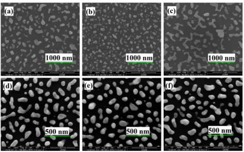
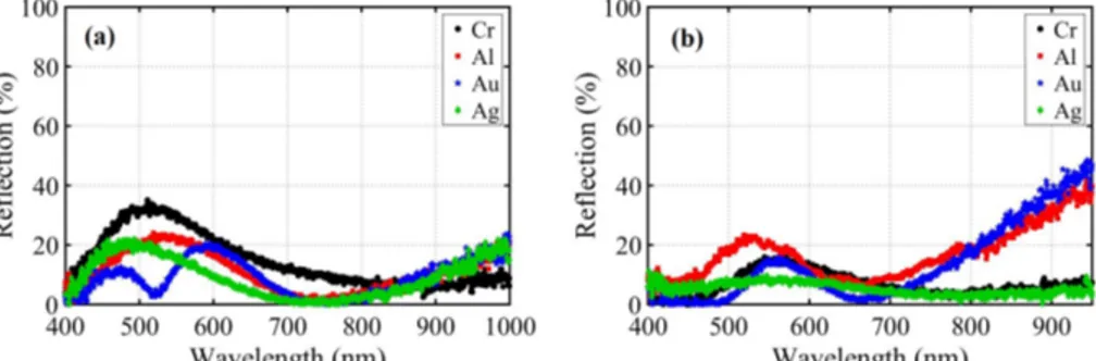
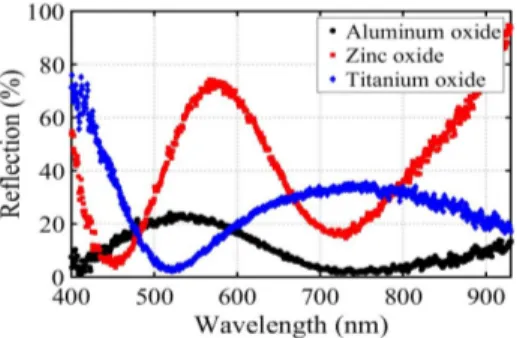
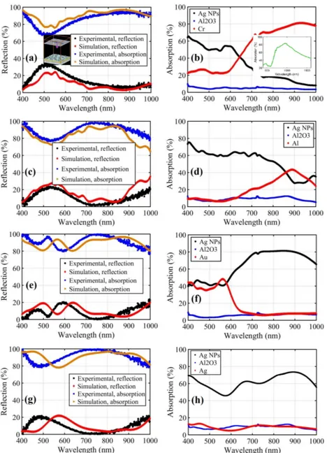
Large area compatible broadband superabsorber surfaces in the VIS-NIR spectrum utilizing metal-insulator-metal stack and plasmonic nanoparticles
Tam metin
Şekil
Benzer Belgeler
Şiirin bütünü düşünüldüğün- de Âşık Abbas Hazretî, Babek’i ve Babek’in Abbasilere karşı verdiği mü- cadeleyi, günümüzde İran Türklerinin verdikleri
coli ile oluşan üriner sistem infeksiyonlarında ampirik tedavide, ampisilin, trimetoprim/sulfametoksazol, amoksisilin- klavulanat, piperasilin, nitrofurantoin ve sefuroksim
Ayr›ca kat›l›mc›lar›n korsan yaz›l›m kullanma hakk›ndaki düflüncelerinin yafllar›na ba€l› olarak de€iflti€i, yaflça büyük olanlar›n korsan yaz›l›m
If suitable values are set for the plant, the system produces high quality water which can be used as potable water. Therefore, the plan with a high-capacity-plant is to put treated
The snake fit to the laser data is referred to as C laser from now on in this text. The snakes fitted to the processed UAM data will be referred to as C i , where i denotes the index
Results of synthetic scenarios 72 and 68 show that for small percentage delay errors, single bounce model locations are in the neighbourhood of first and second scatterer (close
Coupled waveguide modulator relies on the mode coupling between adjacent waveguides. Two identical waveguides are coupled over a distance L, with electrodes placed over the
Vanillin/cyclodextrin inclusion complex nano fibers (vanillin/CD-IC NFs) were successfully obtained from three modi fied CD types (HPβCD, HPγCD and MβCD) in three different
