PROCEEDINGS OF SPIE
SPIEDigitalLibrary.org/conference-proceedings-of-spieLow-frequency noise behavior at
reverse bias region in InAs/GaSb
superlattice photodiodes on
mid-wave infrared
T. Tansel
K. Kutluer
A. Muti
Ö. Salihoglu
A. Aydinli
R. Turan
Low-frequency noise behavior at Reverse Bias Region in InAs/GaSb
Superlattice Photodiodes on Mid-Wave Infrared
T. Tansel
a, K. Kutluer
a, A. Muti
b, Ö. Salihoglu
b, A. Aydinli
b, and R. Turan
aa Middle East Technical University (METU), Department of Physics, 06531 Ankara/Turkey
b Bilkent University, Department of Physics, Advanced Research Laboratory, 06800 Ankara/ Turkey
ABSTRACT
We describe a relationship between the noise characterization and activation energy of InAs/GaSb superlattice Mid-Wavelength-Infrared photodiodes for different passivation materials applied to the device. The noise measurements
exhibited a frequency dependent plateau (i.e. 1/f-noise characteristic) for unpassivated as well as Si3N4 passivated
samples whereas 1/f-type low noise suppression (i.e. frequency independent plateau) with a noise current reduction of
more than one order of magnitude was observed for SiO2 passivation. For reverse bias values below -0.15V, the classical
Schottky-noise calculation alone did not appear to describe the noise mechanism in a SL noise behavior, which shows a divergence between theoretically and experimentally determined noise values. We identify that, the additional noise appears, with and without passivation, at the surface activation energy of < 60 meV and is inversely proportional to the reverse bias. This is believed to be caused by the surface dangling-bonds (as well as surface states) whose response is controlled by the applied reverse bias. The calculated noise characteristics showed a good agreement with the experimental data.
Keywords: Mid-Wave-Infrared Photodiode, Passivation, Noise Characterization, InAs/GaSb, surface activation energy
1. INTRODUCTION
In recent years, Mid-Wavelength-Infrared (MWIR) InAs/GaSb-superlattice (SL) photodetectors are attracting considerable attention due to its promises for new generation infrared detectors having applications in military, industrial, and medical technologies. When compared with the HgCdTe photodiodes which dominate current IR detector technology, MWIR SL photodetectors offer remarkable advantages such as low noise current due to the suppression of Auger recombination [1, 2, 21]. However, in spite of numerous studies on different features SL detectors, the effects of surface leakage current on the detector performance are not well understood. In general, the existence of dangling- bonds at the crystal surface -attributed to the abrupt termination of semiconductor surface- and native oxides on the SL leading to surface leakage current, and that can extremely limit/degrade the SL infrared detector performance. This might cause to form a favorable surface potential for easy carrier transport over the surface [2, 3]. Hence, without proper surface passivation the leakage current is significant, particularly on the mesa side-walls. This is of high importance especially where the detector area approaches the sizes needed for focal- plane -array applications. Consequently, intentional passivation is needed to suppress the leakage current by minimizing/eliminating the states and hence the influence of foreign materials [2]. The relation between surface leakage and the noise properties of the detector needs to be clarified for a complete understanding. Certainly, noise experiments shall guide one to calculate the true specific detectivity as well. The noise figure performance, which is an indicator of the quality of a photodetector, is one of the most sensitively affected parameters by the surface and bulk conditions in semiconductor material [3, 4]. Therefore, in this work, we used the SLs noise characteristics and performed direct measurements of the dark noise current vs. passivation material with a view to understand the effects of dark current and noise on the detector performance.
2. EXPERIMENTAL
In order to study the surface effects on the MWIR InAs/GaSb SL detector structures were obtained from IQE Inc. (with
cut-off wavelength 4.9m at 79 K). The device structures were grown by molecular beam epitaxy on an n-type (001)
GaSb substrate, based on 60-periods n-type/60-periods non- intentionally doped (n.i.d.) active region/90-periods p-type InAs/GaSb SL. Each period in the entire structure consists of 2.85 nm InAs and 3.3 nm GaSb layers with InSb-like
interfaces. GaSb layers in the p-type superlattice period were doped with Be to a level of 1.5 x 1017 cm-3 while the InAs
layers were doped with Te to a level of 5 x 1017 cm-3. The entire SL structure was enclosed by a 20 nm n-type InAs: Te
(5 x 1017cm-3) top and a 1 μm thick p-type GaSb: Be (1 x 1017 cm-3) bottom contact layers.
To protect the sample surface (with a mesa size of 400 m x 400 m) from ambient atmosphere, surface passivation
was realized directly after the wet etching (which uses phosphoric and citric acid solutions) with a 230 nm SiO2 or 150
nm Si3Ni4 coating applied by Plasma Enhanced Chemical Vapor Deposition (PECVD) method [22].
A Ti-Au (30nm/300nm) bi-layer was evaporated onto the top and back surfaces of the photodiodes for ohmic contacts. In order to measure the temperature dependent dark current or resistance- area product (RA), a CTI Cryogenics helium cryostat (22C Cryodyne Refrigeration System) was employed as cold head and a Keithley (Keithley 6487) picoammeter was used to apply the DC bias (Vbias) to the detector and to read the output current.
For the dark current noise characterizations, the specimen was placed in a cryostat and cooled down to 79 K using liquid nitrogen. During the measurements, all instruments including the low noise current amplifier (Stanford Research Systems, SR570), cryostat and FFT spectrum analyzer (Stanford Research system, SR760) were placed inside a shielded
box. We subtracted the system noise from the measured total noise (in A/Hz) to obtain the intrinsic detector noise6.
Here, the intrinsic detector noise sources consist of white noise as well as 1/f-noise [7]. Schottky-noise (I2sn= 2qI) and
Johnson-noise (I2jn= 4kBT/Rd) together form the ‘white noise’ (I2sn + I2jn) of the detector, where kB the Boltzmann
constant, T the temperature, Rd the dark differential resistance, q the electronic charge constant, and I the dark current.
The 1/f -noise is inversely proportional to frequency and so it is above the white noise level at low frequencies. In general, this type of 1/f-noise is particularly sensitive to surface imperfections [3,4].
3. RESULT AND DISCUSSION
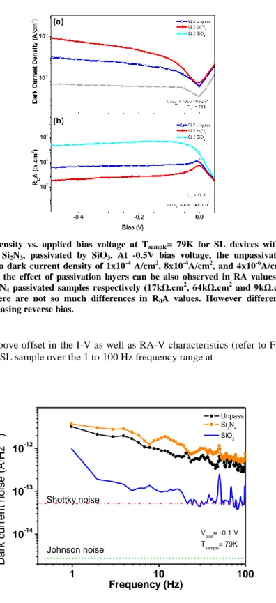
The dark current–voltage (I–V) characteristics at Tsample= 79K for SL diodes with variable passivation layers and
unpassivated surface are shown in Figure 1. At Vbias= -0.5V the unpassivated and Si3N4 passivated samples exhibits a
maximum dark current density of, ~10-5 and ~10-4A/cm2 respectively, while the SiO2 passivated device shows a nearly
constant line with a dark current density of ~10-7A/cm2 at the overall reverse bias regime.
The dark current density was seen to increase approximately proportional to Vbias for the unpassivated and Si3Ni4
passivated devices. However, in comparison, the best results were presented by the SiO2 passivated device with the dark
current density reduced by up to 2 to 3 orders of magnitude. From this follows, the SiO2 passivation is likely to be the
Figure 1. Dark current density vs. applied bias voltage at Tsample= 79K for SL devices with (a) no intentional
passivation, passivated by Si2N3, passivated by SiO3. At -0.5V bias voltage, the unpassivated, Si3N4 and SiO2
passivated samples exhibit a dark current density of 1x10⁻⁴ A/cm2, 8x10⁻⁴A/cm2, and 4x10⁻⁶A/cm2, respectively. RA
vs. Bias results in part (b), the effect of passivation layers can be also observed in RA values at Tsample= 79K for
unpassivated, SiO2, and Si3N4 passivated samples respectively (17kΩ.cm2, 64kΩ.cm2 and 9kΩ.cm2). As in the dark
current density results, there are not so much differences in R0A values. However differences between values
increase drastically with creasing reverse bias.
In order to appreciate the above offset in the I-V as well as RA-V characteristics (refer to Figure 1), we studied the dark noise characteristic of the SL sample over the 1 to 100 Hz frequency range at
Vbias= -0.1V and Tsample= 79K.
1 10 100 10-14 10-13 10-12 Unpass Si 3N4 SiO2 Johnson noise Dark c urr ent no is e (A Hz 0 .5 ) Frequency (Hz) Vbias= -0.1 V Tsample= 79K Shottky noise
Figure 2 shows the noise spectra for unpassivated, and SiO2 passivated SLs. For SiO2 passivated sample, the
frequency independent plateau in the 20-100 Hz range is due to white-noise. This is well matched with the calculated
theoretical Schottky-noise (Isn= 5 x 10-14A/Hz), and thus indicates a good passivation level.
The 1/f-noise is suppressed and the dark noise current is reduced by one order of magnitude (at Vbias= -0.1V) against to
unpassivated SL. The effect of surface states and foreign materials seem to be suppressed along the exposed mesa
Surface through SiO2 passivation. In contrast, the noise values for other materials (unpassivated as well as Si3N4
-passivated SL) reveal frequency dependent behaviors in the same frequency range, which indicate a 1/f-noise
contribution. The existence of the 1/f-noise contribution approves that Si3N4 passivation did not lead to an enhancement
but rather degradation of the sample quality. The dark noise current in an ordinary diode often increases under reverse bias due to 1/f-noise in the surface leakage current [9].
The noise spectra of SiO2 passivated detector displayed in Figure 3 do not exhibit additional noise at -0.1V at ~30Hz
(i.e. the dominant noise is Schottky-noise), but at -0.5 V an additional noise seems to increase with an applied reverse
Vbias. This appears to have resulted from an additional frequency dependent noise (potentially 1/f-noise). From the
observed interdependence, such 1/f-noise should be related to the surface leakage current. The disagreement (seen in Figure 3) with the theoretical Schottky noise expectation (by a factor of ~ 3) at -0.5 V is possibly caused by the 1/f-noise which further increases with the reverse bias-which in fact is in agreement to that reported in Ref. 6 and 7.
1 10 100 10-14 10-13 10-12 -0.1V -0.5V Dark c urr en t n oi s e (A Hz 0 .5 ) Frequency (Hz) Shottky noise 1/f noise
Figure 3. Noise spectra as function of frequency for SiO2 passivated devices at -0.1V and -0.5V (temperature 79K). The fitted strait line and dotted lines indicates the 1/f-noise behavior.
In order to verify the effect of surface leakage current, we performed dark I-V measurements on a series of diodes with different perimeter-to-area ratio, since the surface resistivity is directly proportional to the surface-dependent
leakage current of the diodes for unpassivated SL [8]. However, the measured surface resistivity of ~1x106 cm for SiO2
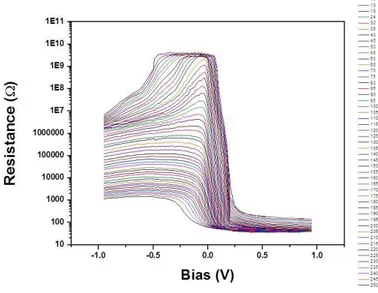
passivated SL diode at the unbiased condition is relatively too large to conclude to a self-initiated surface leakage current. Another method to obtain the dominating mechanism at the considered temperature range is to measure the RA vs. reciprocal temperature (1000/T) which can separate the bulk current from surface current dynamic of the diodes [10]. In order to do this, first of all it should be verified that at temperature range around 80 K, the dominant current mechanism is surface limited current. Temperature dependent I-V measurements and Arrhenius Plot analysis provides evidence for dominated current mechanisms. In Figure 4, results of temperature dependent I-V measurements in the
form of resistance vs. bias are given for temperature range from 11 to 250 K for SiO2 passivated SL sample. The effect
1E11 1E10 1E9 1E8 -. 1E7 -1000000-. 100000 10000 1000 100 -10 -1.0 0.0 0.5 1.0 Bias (V)
Figure 4. Resistance vs. Bias results from 11K to 250K temprature range for SiO2 passivated sample.
This measurement is also realized for unpassivated and Si3N4 passivated SL samples. For each temperature, resistance
values at specific bias values are extracted from the data to plot resistance as a function of inverse temperature graph as presented in Figure 5. In this graph, 3 different current mechanisms are plotted for different temperature regions.
6 8 10 12 101 103 105 107 200 150 100
T (K)
50RA
(
cm
2)
1000/T (K
-1)
(a) (b) (c) Diffusion GR Surface Limited V bias= -0.1VFigure 5. Resistance-area product vs. Temperature dependent for the SL device passivated with SiO2 at the different
Bias voltages of - 0.1 and - 0.5 V.
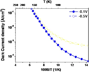
O
O-At temperature values higher than 200 K, thermal energies of charge carriers are sufficient to realize band-to-band transition. Therefore the first slop of Arrhenius plot indicates the diffusion current mechanism.
From the slope of Figure 5, activation energy (Eact) required in band-to-band transition can be calculated which is also
equal to the band gap of the device obtained from optical measurements. It is found 0.24 eV, very close to optical
measurements. The GR Eact is 0.12 eV (e.g. for SiO2-passivated sample), which is half of the band gap as expected in the
literature [15].
For different passivation layers, a different deviation from Arrhenius fit was observed for 65 - 95 K. In this temperature
range, the dominating current mechanism is the surface limited current [10], which is somewhat suppressed in the SiO2
sample in contrast to other samples at zero bias. In other words, the deviation which may corresponds to surface leakage current from the Arrhenius fit to the I-V curves for different reverse biases in the temperature range of 65 - 95 K (see Figure 6).
Figure 6. Dark current density as function of inverse Temperature for passivated by Si3N4samples at the different bias
In regards to Ref.10, the higher the reverse bias the more the surface states will form, since surface leakage current is a
direct result of states, and consequently the surface states are proportional to the applied reverse Vbias. Therefore, by
considering the results of Figure 3 and Figure 5, we can relate the surface states to the 1/f-noise as well as additional noise in Figure 8.
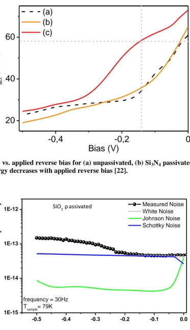
In order to better understand the influence of bias voltage on surface states, we investigate that in terms of the activation energy. The activation energy of the current limiting factors at different reverse bias values can be determined from the slope of the linear fit to ln(RA) vs. 1000/T for different reverse voltages (see Figure 7) [14,15].
Figure 6 shows the Eact vs. reverse Vbias for all SL diodes. Clearly, an inverse dependence is seen between Eact and
reverse Vbias. Lowering Eact implies that the increment of the surface states is caused by the reverse bias voltage and this
can be attributed to the appearance of additional noise or 1/f-noise in the experimental results. This observation is also valid for the sample with no passivation.
-0.5 -0.4 -0.3 -0.2 -0.1 0.0 1E-14 1E-13 1E-12 D a rk c u rr e n t n o is e ( A Hz 0 .5 ) Measured Noise White Noise Johnson Noise Schottky Noise Bias (V) frequency = 30Hz Tsample= 79K -0.5 -0.4 -0.3 -0.2 -0.1 0.0 1E-15 1E-14 1E-13 1E-12 D a rk c u rr e n t n o is e ( A Hz 0 .5 ) Measured Noise White Noise Johnson Noise Schottky Noise Bias (V) frequency = 30Hz Tsample= 79K SiO2 passivated
-0,4
-0,2
0
20
40
60
E
a c t(meV
)
Bias (V)
(a)
(b)
(c)
Figure 7. Activation energy vs. applied reverse bias for (a) unpassivated, (b) Si3N4 passivated and (c) SiO2 passivated
devices. The activation energy decreases with applied reverse bias [22].
Figure 8. Dark current noise with respect to bias voltage for SiO2 passivated SL3 sample
In the following, for sake of clarity/brevity, we discuss the experimental results obtained on SiO2 passivated
samples. A cross correlation between Figure 7 and Figure 8 indicates that for Eact higher than 60 meV the Schottky-noise
dominates at the smaller reverse Vbias than - 0.1 V. However, for Eact approximately smaller than 60 meV, the
dominating type is 1/f-noise at the higher reverse Vbias than -0.15 V. Further, it results in much higher noise in the
detector (i.e. at ~30 Hz frequency) as seen in Figure 3 as well as in Figure 8.
More specifically, the value of surface potential (energy barrier) can be adjusted via bias voltage (by an amount of electrostatic energy) which alters the surface charge equilibrium between the surface states and space charges. With increasing reverse bias, a decrease in the activation energy barrier is expected and so more states, as well as surface
surface, no additional current flow can be seen in I-V characteristic.This means that the charge carriers do not leave the device, although they flow to the surface, they are lost on the surface and create noise. But recombination noise is directly related with the carrier concentration on the surface.
The value of carrier concentration (ns) is strongly dependent on the operation bias voltages at constant temperature,
and leads to the exponential behavior of Eact, which results in the analytical expression ns ~ exp(-Eact/kBT) where ns is the
charge carrier concentrations [15,16]. By assuming, ns are proportional to the leakage current Ilc with a proportionality
factor of Ic. The final equation is formed as Ilc = Icexp(-Eact/kBT).
Under the assumption that above process behaves as a photovoltaic device mechanism, hence to estimate the surface
leakage current noise Ilcn similar like Schottky-noise calculation for p-n junction diodes [17, 19], is given by
T k E qI I B act c lcn 2 exp 2 (2)
By claiming that all the noise sources (i.e.IJN, ISN and Ilcn) are statistically independent, the total noise Itotal is then found
as
I2total= I2SN + I2JN + I2lcn (3)
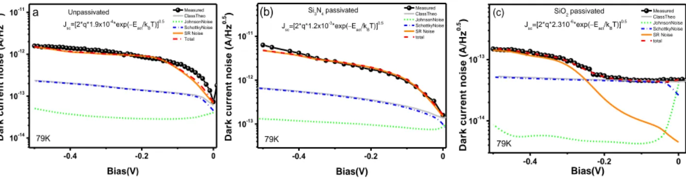
To demonstrate the validity of equation (3), fits of experimental noise dark current were made in the voltage range 0- 0.5 V to identify the bias-dependent dominant noise dark current component.
The parameters were deduced from experimental data such as Eact, ISN, IJN and Ic. Wherein, the Ic was deduced from I2lcn
(i.e., is formed as I2lcn = I2total- I2SN - I2JN) vs. Eact plot graphically by curve fitting, i.e., curve fitting was used to determine
the value of Ic which is the intercept (where Eact is zero) divided by 2q at around 79K [20]. More precisely, Ic is the total
number of surface charge carrier concentration (which may lead to a recombination) per unit time and exp(-Eact/kBT) is
the probability that any given surface carrier concentration will result in a recombination in the surface states. The temporal fluctuation in recombination rate per unit time itself leads to frequency dependence behavior which in turn
results in surface recombination noise Ilcn. We propose inverse frequency dependence, but it is not clear exactly how the
frequency dependence of Ic varies; therefore, further investigations are needed.
The plots between experimental (sphere) and fitted (dashed) lines also the surface leakage noise (line) are shown in
Figure 9 for unpassivated and SiO2, Si3N4 passivated SL diodes, respectively.
Figure 9. Total dark noise current as function of the bias for the SL device (a) unpassivated, passivated with (b) Si4N3, (c)
SiO2, The dashed line shows the calculated Shot-noise; the dotted line represents the Johnson-noise; dashed dotted line
demonstrations the calculated surface noise, the lines exhibits the Itotal fitted and the white noise
The noise fit is in a good agreement to the experimental results. This agreement between the experimental data and the fit proves that the additional dark noise current is surface recombination current. Thus, it can be concluded that an
increase in reverse Vbias lowers the activation energy barrier at the interfaces exponentially hence generate higher states
that contributes to a 1/f-noise as well as additional to the noise appeared.
-0.4 -0.2 0 10-13 10-12 10-11 Jsc=[2*q*1.2x10 -3 *exp(Eact/kBT)] 0.5 D a rk c u rr e n t n o is e ( A Hz 0 .5) Bias(V) Measured ClassTheo JohnsonNoise SchottkyNoise SR Noise total 79K Si3N4 passivated (b) -0.4 -0.2 0 10-14 10-13 10-12 10-11 Jsc=[2*q*1.9x10⁻⁴*exp(E act/kBT)] 0.5 D a rk c u rr e n t n o is e ( A Hz 0 .5) Bias(V) Measured ClassTheo JohnsonNoise SchottkyNoise SR Noise Total 79K Unpassivated a -0.4 -0.2 0 10-14 10-13 J sc=[2*q*2.310 -6*exp(E act/kBT)] 0.5 D a rk c u rr e n t n o is e ( A Hz 0 .5) Bias(V) Measured ClassTheo JohnsonNoise SchottkyNoise SR Noise total 79K SiO2 passivated (c)
SUMMARY AND CONCLUSION
In conclusion, we studied the dark current and noise characteristics in MWIR InAs/GaSb SL photodiodes with
and without surface passivation. It was shown that SiO2 passivation decreases the dark current by up to two orders of
magnitude, which is attributed to the effective suppression of surface leakage currents. The noise measurements revealed the absence of intrinsic 1/f-noise (as well as a noise reduction with one order of magnitude) above 40-30 Hz
and Shottky-limited behavior up to VBias= ~ -0.15 V. Despite the classical theoretical noise expectation below VBias=
-0.15 V a difference was observed between the experimental and theoretically calculated Shottky-noise, with a divergence factor of ~3. The origin of the difference is attributed the presence of surface leakage current, which
emanated from the reduction in surface barrier height at the SL interface by the applied reverse Vbias. The leakage
current was shown to result from a surface recombination mechanism, due to the relationship between 1/f-noise and
the RA vs. 1/T deviations (at a given reverse Bias). This helped to explain the increase in 1/f-noise with reverse Vbias.
Indeed, the appearance of additional frequency noise associated with the surface states is consistent with the observation of surface leakage current that is also attributed to an electrical activity of surface states.
REFERENCES
[1] A. Rogalski, Science ProgrRess in Quantum Electronics, 27, 59-210 (2003). [2] R. Chaghi, C. Cervera, H. Ait-Kaci, P. GrRech, J. B. Rodriguez, and P. Christol, [3] B.K Jones, Adv. Electron. Electron Phys. 87, 201-257 (1993)
[4] Weissman M B,, 1/f-noise’’ Rev. Mod. Phys. 60, 537 (1988)
[5] A. Gin, Y. Wei, J. Bae, A. Hood, J. Nah, M. Razeghi, Thin Solid Films, 447, 489–492 (2004). [6] T. Tansel et. al. IEEE Photon. Technol. Lett., 24, 9, (2012)
[7] K. Jaworowicz, I. Ribet-Mohammed, C. Cervera, J.B. Rodriguez, and P. Christol, IEEE Photonics Technology Letters, 23, 4, (2011)
[8] E. Pils, M.N. Kutty, S. Myers, H.S. Kim, N. Gautam, L.R. Dawson, S. Krishna, Infrared Physics &Technology 54, 252-257 (2011).
[9] Antoni Rogalski, Krzystof,, Narrow-gap semiconductor photodiodes SPIE Press, Bellingham, Washington. [10] B.M. Nguyen et. al. Appl. Phys. Lett. 94, 223506 (2009)
[11] E.K. Huang, D. Hoffman, B. Nguyen, P. Delaunay, M. Razeghi, Appl. Phys. Lett., 94, 053506, (2009).
[12] A. Soibel, D. Z.-Y. Ting, C. J. Hill, M. Lee, J. Nguyen, S. A. Keo, J. M. Mumolo, S. D. Gunapala, Appl. Phys. Lett. 96,111102 (2010)
[13] H. S. Kim, E. Plis, A. Khoshakhlagh, S. Myers, N. Gautam, Y. D. Sharma, L. R. Dawson, S. Krishna, S. J. Lee, and S. K. Noh, Appl. Phys. Lett. 96, 033502 (2010).
[14] G. Marre, B. Vinter and V. Berger, Semicond. Scie. Technol. 18, 284-291 (2003) [15] Shin Mou, Jian V. Li, and Shun Lien Chung J. Appl. Phys. 102. 066103 (2007)
[16] M. Weinelt, m. kutschera,r. Schmidt,c. orth, t. fauster,m. rohlfing Appl. Phys. A 80, 995–1003 (2005)
[17] Charles A. Vergers,, Handbook of Electrical Noise: measurement and Technology’’ hand book, 2 Sub edition (1987).
[18] E. Bendada. K. Rais, P. Mialhe and J. P. Charles Active and passive Elec. Comp., 21, 61-71, (1998).
[19] John David Vincent,, Fundamentals of Infrared Detector Operation and Testing’’, Wiley Series in Pure and Applied Optics, (1990)
[20] Tunay Tansel, Kutlu Kutluer, Abdullah Muti, Omer Salihoglu, Atila Aydinli, and Rasit Turan Applied Physics Express 6, 032202 (2013)
O. Salihoglu, A. Muti, K. Kutluer, T. Tansel, R. Turan, Y. Ergun, and A. Aydinli: Appl. Phys. Lett. 101 (2012) 073505.