INTEGRATED MICROFLUIDIC
SYSTEMS FOR DROPLET DETECTION
AND SORTING
A THESIS SUBMITTED TO
THE GRADUATE SCHOOL OF ENGINEERING AND SCIENCE OF BILKENT UNIVERSITY
IN PARTIAL FULFILLMENT OF THE REQUIREMENTS FOR THE DEGREE OF MASTER OF SCIENCE
IN
MATERIALS SCIENCE AND NANOTECHNOLOGY
By
Pelin Kubra Isgor
ii
I certify that I have read this thesis and that in my opinion it is fully adequate, in scope and in quality, as a thesis for the degree of Master of Science.
Assist. Prof. Dr. Çağlar Elbüken (Supervisor)
I certify that I have read this thesis and that in my opinion it is fully adequate, in scope and in quality, as a thesis for the degree of Master of Science.
Prof. Dr. Haluk Külah
I certify that I have read this thesis and that in my opinion it is fully adequate, in scope and in quality, as a thesis for the degree of Master of Science.
Assist. Prof. Dr. Yegân Erdem
Approved for the Graduate School of Engineering and Science:
Prof. Dr. Levent Onural Director of Graduate School
iii
ABSTRACT
INTEGRATED MICROFLUIDIC SYSTEMS
FOR DROPLET DETECTION AND SORTING
Pelin Kubra Isgor
M.S. in Materials Science and Nanotechnology
Supervisor: Assist. Prof. Dr. Caglar Elbuken
September 2015
Microdroplet based microfluidic systems have gained a lot of attention during the last decades due to enhanced analytical performance, low cost and high-throughput. One of the fundamental requirements of a droplet based system is detection of droplets. Capacitive sensing of droplets have been used for droplet detection, however they lack the required sensitivity for droplet content detection. Here a portable, low cost, scalable and highly sensitive droplet content detection system is demonstrated using coplanar electrodes. The designed microfluidic system enables droplet content modification on the run. While changing droplet content, i.e., dielectric content, capacitive signal amplitude is measured. The system resolves 3 unit of dielectric permittivity. 5% material change in droplet is detected.
Following droplet content detection, sorting of laden droplets enables further experimentation with material of interest in the droplet. Dielectrophoresis is a commonly used method for droplet sorting. Dielectrophoretic sorting of droplets is demonstrated using two dimensional and there dimensional electrodes.
iv
Low cost and portable electronic components are integrated with microfluidic devices for droplet content detection and sorting using microfabricated electrodes. The cost and signal to noise ratio of the system are aimed to be decreased by implementing detection and sorting system on a printed circuit board. Sensing and sorting electrodes are fabricated and all of the electronic components are placed on a printed circuit board. Microchannels are reversibly placed over electrodes, therefore the platform becomes reusable. This feature of the system enables various experimentation using microdroplets on the same base platform.
This approach will lead to microfluidic systems that are programmable and easy-to-use by means of off-the-shelf and low cost electronic components.
Keywords: droplet content sensing, droplet sorting, printed circuit board,
v
ÖZET
DAMLACIK TANIMA VE AYRIŞTIRMA İÇİN
ENTEGRE MİKROAKIŞKAN SİSTEMLER
Pelin Kübra İşgör
Malzeme Bilimi ve Nanoteknoloji Bölümü Yüksek Lisans
Tez Yöneticisi: Yrd. Doç. Dr. Çağlar Elbüken
Eylül 2015
Son zamanlarda, microdamlacık temelli mikroakışkan sistemler geliştirilmiş işlem yetenekleri, ucuz olmaları, ve kısa zamanda pek çok deneyi gerçekleştirebiliyor olmaları nedeniyle ilgi odağı olmaya başladı. Damlacık temelli sistemlerin gerekliliklerinden bir tanesi de damlacıkların sistem içinde tanınmasıdır. Literatürde damlacıkların kapasitif olarak belirlenmesine ait çalışmalar olmasına rağmen, bu çalışmalar damlacığın içinde yer alan malzemeyi tanımlayabilmek için gereken hassasiyete sahip değildir. Aynı düzlemde konumlandırılan elektrotlar ile taşınabilir, ucuz, ölçeklenebilir ve oldukça hassas bir damlacık tanıma sistemi bu tezde gösterilmiştir. Tasarlanan mikroakışkan sistem damlacık oluşurken içindeki malzemenin değiştirilmesine olanak sağlamaktadır. Damlacığın içeriği değiştirilirip, kapasitif olarak damlacıktan sinyal alınmıştır. Bu sistemim çözünürlüğü 3 birim dielektrik sabiti kadardır. Ayrıca, damlacığın içindeki yüzde beşlik değişim sistem tarafından algılanabilmektedir.
Damlacığın içinin tanınabiliyor olmasına ek olarak, içerisinde ilgilenenilen malzeme bulunan damlacıklar ayrıştırılarak daha fazla deneysel işlemin yapılmasına olanak sağlamaktadır. Damlacık ayrıştırma için dielektroforesis
vi
yaygın olarak kullanılan bir yöntemdir. Bu tezde iki boyutlu ve üç boyutlu elektrotlar kullanılarak damlacıkların dielektroforetik olarak ayrıştırılması gösterilmiştir.
Ucuz ve kolaylıkla taşınabilir tümleşik devreler damlacık içini tanıma ve damlacığı ayrıştırma işlemleri için mikroakışkan sistemlerle birleştirilmiştir. Bunun için mikro boyutta üretilen elektrotlar kullanılmıştır. Bütün sistem baskı devre kartına taşınarak, maliyet ve sinyalin gürültüye oranının düşürülmesi amaçlanmıştır. Damlacık tanıma ve ayrıştırma için kullanılan elektrotlar ve bütün tümleşik devreler baskı devre kartına taşınmıştır. Mikrokanallar sistemin yeniden kullanılmasına olanak sağlayacak şekilde elektrotların üstüne yerleştirilmiştir. Sistemin bu özelliği, aynı platform üstünde damlacıkları kullanarak çeşitli deneylerin yapılmasına olanak sağlamaktadır.
Bu teknik kolayca bulunabilen ve oldukça ucuz elektronik parçaları kullanıyor olması sayesinde mikroakışkan sistemleri programlanabilir ve kolayca kullanılabilen platformlara dönüştürecektir.
Anahtar sözcükler: damlacık içeriği tanıma, damlacık ayrıştırma, baskı devre
vii
Acknowledgement
I would like to acknowledge and thank European Union Marie Curie 7th Frame Programme (Project no. 322019) for the financial support throughout my M.Sc. studies. Also, I would like to thank TUBITAK (Project no. 213S127) for partial financial support.
viii
Dedicated to my family
Mevlüde, Hasan and Aylin
and my grandmother
Cevriye
ix
Table of Contents
C
HAPTER1
I
NTRODUCTION... 1
1.1MOTIVATION OF THE THESIS ... 1
1.2OVERVIEW OF THESIS ... 3
C
HAPTER2
S
CIENTIFICB
ACKGROUND... 4
2.1WHAT IS MICROFLUIDICS ? ... 4
2.2DROPLET-BASED MICROFLUIDIC SYSTEMS ... 6
2.2.1DROPLET FORMATION ... 6
2.2.3DROPLET BREAK-UP ... 9
2.2.4DROPLET COALESCENCE ... 9
C
HAPTER3
F
ABRICATION ANDC
HARACTERIZATIONM
ETHODS... 11
3.1FABRICATION OF COPLANAR ELECTRODES AND PASSIVATION LAYER ... 11
3.1.1PHOTOLITHOGRAPHY ... 12
3.1.2THIN FILM METALLIZATION ... 13
3.1.2.1SPUTTERING ... 13
3.1.2.2.THERMAL EVAPORATOR ... 14
3.1.3DIELECTRIC FILM COATING ... 15
3.1.3.1PLASMA ENHANCED CHEMICAL VAPOR DEPOSITION (PECVD) 15 3.2FABRICATION OF MICROCHANNEL MOLD ... 15
3.3SOFT LITHOGRAPHY ... 19
3.4CHARACTERIZATION METHODS ... 22
3.4.1ATOMIC FORCE MICROSCOPY (AFM) ... 22
3.4.2VARIABLE ANGLE SPECTROSCOPIC ELLIPSOMETER ... 23
3.4.3STYLUS PROFILOMETER ... 24
C
HAPTER4
D
ROPLET CONTENT DETECTION USING INTEGRATED CAPACITIVE SENSORS... 25
4.1INTRODUCTION ... 25
4.2CAPACITIVE DETECTION THEORY ... 27
x
4.3.1DESIGN OF THE DEVICE ... 32
4.3.2FABRICATION OF THE DEVICE ... 33
4.4EXPERIMENTAL PROCEDURE ... 34
4.4.1EXPERIMENTAL SET-UP ... 34
4.4.2EXPERIMENTAL PROCEDURE ... 36
4.5RESULTS AND DISCUSSION ... 40
4.5.1ANALYTICAL MODEL COMPARISON... 40
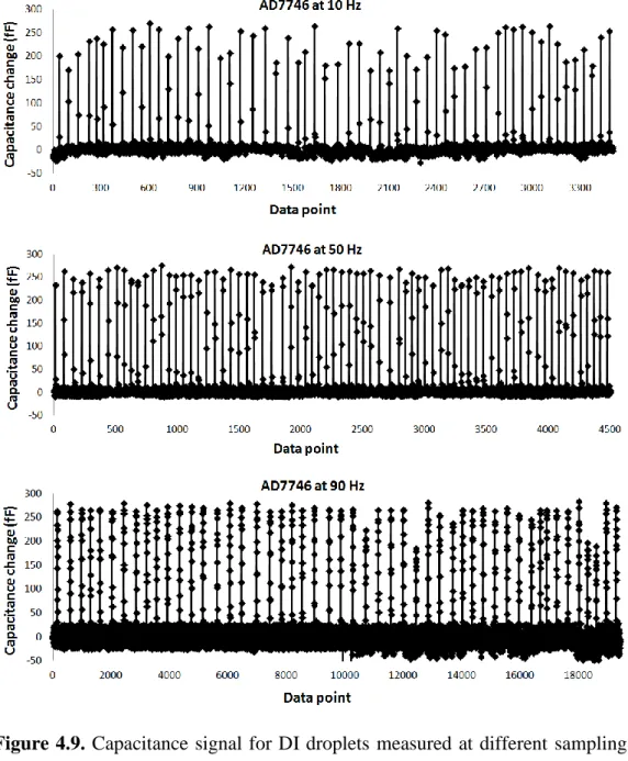
4.5.2CHOOSING THE DATA RATE ... 42
4.5.3FINDING PROPER ELECTRODE WIDTH ... 43
4.5.4SIGNAL ENHANCEMENT THROUGH THINNER PASSIVATION LAYER . 45 4.5.5DROPLET DIELECTRIC CONTENT MEASUREMENT ... 47
4.5.6VERIFICATION ... 50
4.6POSSIBLE FUTURE APPLICATIONS ... 51
4.7CONCLUSION ... 53
C
HAPTER5
D
ROPLETS
ORTINGU
SING2D
C
OPLANAR AND3D
EG
AI
NE
LECTRODES... 54
5.1INTRODUCTION ... 54
5.2DIELECTROPHORESIS (DEP)THEORY ... 57
5.3DESIGN AND FABRICATION ... 63
5.3.12DDEP DEVICE DESIGN AND FABRICATION ... 63
5.3.23DEGAIN ELECTRODE AND CHANNEL DESIGN AND FABRICATION 67 5.4EXPERIMENTAL PROCEDURE ... 69
5.5RESULTS ... 72
5.6CONCLUSION ... 75
C
HAPTER6
D
ROPLETD
ETECTION ANDS
ORTING ON AP
RINTEDC
IRCUITB
OARD(PCB) ... 76
D
ROPLETD
ETECTION ANDS
ORTING ON AP
RINTEDC
IRCUITB
OARD(PCB) ... 76
6.1INTRODUCTION ... 76
xi
6.3DESIGN AND FABRICATION ... 84
6.4EXPERIMENTAL PROCEDURE ... 89
6.5RESULTS ... 91
6.5.1ON-PCB DROPLET CONTENT DETECTION ... 91
6.5.2COMSOLSIMULATION RESULTS ... 93
6.6CONCLUSIONS ... 100
C
HAPTER7
C
ONCLUSIONS... 101
7.1CONCLUSIONS ... 101 7.2FUTURE WORK ... 102 7.3CONTRIBUTIONS ... 103B
IBLIOGRAPHY... 104
xii
List of Figures
Figure 3.1. Schematic of mold fabrication using SU-8 negative photoresist ... 19
Figure 4.1. Schematic of the system studied by Chen et al. [33] ... 28 Figure 4.2. Schematic of the system studied by Otter [34]. ... 29 Figure 4.3. Illustration of the capacitance formed by coplanar electrodes. a)
Field lines through the passivation layer, microchannel and PDMS bulk. b) Capacitances through passivation layer (Cp) and microchannel (Cch). Dielectric
permittivities of materials are; εr_water 80, εr_oil 2.5, εr_PDMS 2.5, εr_SiO2
3.85. Effective width of the electrodes is shown as weff. ... 31
Figure 4.4. Schematic of the microfluidic device. The insets show the (a)
droplet generation region and mixing region, (b) detection region. ... 32
Figure 4.5. Photograph of the fabricated microfluidic device. Channels were
filled with dye solutions for clarity. ... 34
Figure 4.6. a) Images of the droplet formation and their travel along the
serpentine section in our system. b) Droplets before the mixing region. c) Droplets after mixing region, completely mixed. ... 35
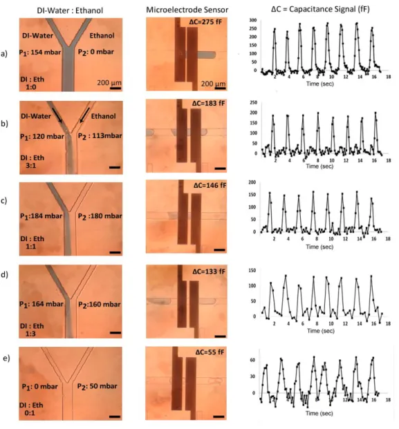
Figure 4.7. Capacitance signal for varied DI ethanol mixtures (a) only DI, (b)
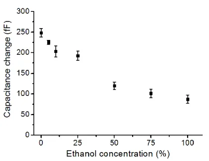
25% ethanol, (c) 50% ethanol, (d) 75% ethanol, (e) only ethanol. The real-time capacitance signal amplitude was displayed through the LabView interface and recorded when droplet enters to the detection region. Each peak corresponds to a single droplet in the sensing region. The plots show the data for 17 seconds. 38
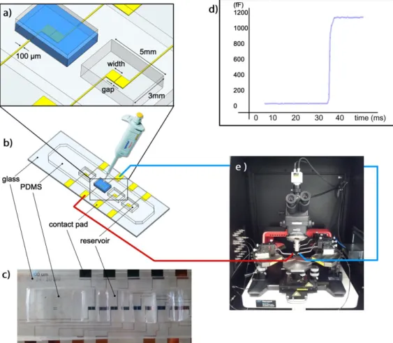
Figure 4.8. Capacitance measurement system for verification purposes: (a)
Close-up view of the electrodes and the reservoirs. Capacitance change is measured by pipetting 50 µl of solution, (b) the schematic of the complete
xiii
device with multiple electrodes, (c) photograph of the fabricated device, (d) exemplary capacitance change plot, (e) probe station for electrical connections. ... 39
Figure 4.9. Capacitance signal for DI droplets measured at different sampling
rates of AD7746. ... 43
Figure 4.10. Capacitance change for electrodes with varying width. The
coplanar electrodes were passivated by 375 nm thick SiO2. The results were
averaged over 50 droplets. ... 44
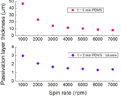
Figure 4.11. PDMS and toluene thinned PDMS thickness. PDMS thickness
(red, square) for 5 min. spinning time and PDMS:toluene, 1:3 (w/w) thickness (blue, diamond) for 2 min. spinning time. ... 45
Figure 4.12. Capacitance change recorded using the semiconductor parameter
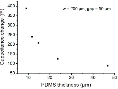
analyzer for DI water at different PDMS passivation layer thicknesses. ... 47
Figure 4.13. Solution dependent capacitance signal amplitudes obtained from
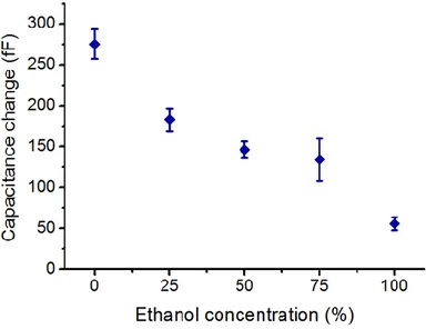
Figure 4.7. Error bars denote one standard deviation across 50 droplet peaks. Coplanar electrodes that have width of 200 µm and gap of 50 µm were used. The electrodes were passivated with 360 nm SiO2. ... 48
Figure 4.14. Calibration plot obtained by pre-mixed solutions. Error bars
denote one standard deviation across 50 droplet peaks. ... 49
Figure 4.15. Capacitance change recorded using the semiconductor parameter
analyzer. 50 µl droplets were precisely pipetted onto the 375 nm SiO2
passivated electrodes using the pre-mixed DI water ethanol solutions. ... 51
Figure 4.16. (Top image) Each peak corresponds to a single cell flowing past
to electrodes. (Bottom image) Distribution of cell capacitance from 2 DNA phase (G0/G1) to 4 DNA phase (G2/M). Reprinted (adapted) with permission
xiv
from ref. [39] (Copyright 2000 Proceedings of the National Academy of Sciences). ... 52
Figure 5.1. Microscope image of DEP device designed by Ahn et al. a) The
dark gray areas are ITO electrodes. The lower and side electrodes are for applying ground and voltage, respectively. White area represents the energized electrodes. b) Droplets flow to left channel when left electrode is energized. c) Droplets flow to right channel when right electrode is energized. Reprinted (adapted) with permission from ref. [46]. (Copyright 2006 American Physics Society). ... 56
Figure 5.2. Polarizable particle response to (A) uniform (B) non uniform
electric field. Reprinted (adapted) with permission from ref. [42]. (Copyright 2006 Elsevier). ... 57
Figure 5. 3 a) 2D DEP electrodes that are bonded to flow focusing device with
side junctions. b) 3D microscope photograph that shows microchannel bifurcation ... 64
Figure 5. 4. a) 2D DEP electrodes that are bonded to flow focusing device. b)
3D microscope photograph that shows microchannel bifurcation, after bifurcation channels do not expand. ... 66
Figure 5. 5. Photograph of the PMMA stage. A PIC and a connector is
integrated to PMMA in order to provide connection between DC to AC inverter and 2D DEP device. ... 67
Figure 5. 6. a) 3D DEP electrodes that are bonded to flow focusing device. b)
3D microscope photograph that shows microchannel bifurcation, after bifurcation channels do not expand. EGaIn was injected to microchannels in order to fabricate 3D DEP electrodes. ... 69
xv
Figure 5. 8. a) 2D DEP set-up. b) Close-up view of 2D DEP device. c)
CXA-M10L-L DC to AC inverter. ... 71
Figure 5.9. On-demand droplet sorting using 3D electrodes. When the AC
signal is off, droplets go either channel. When AC signal is given to the upper electrodes, droplets are sorted towards the upper channel, vice versa. Scale bar is 500 µm. ... 73
Figure 5. 10. Frequency dependent real part of Clausius-Mossotti factor
calculation at varying droplet conductivities. ... 74
Figure 6. 1. COMSOL snapshot of DEP electrodes that have 2 µm height in z
direction. ... 82
Figure 6. 2. COMSOL snapshot of DEP electrodes that have 80 µm height in z
direction. ... 82
Figure 6. 3. COMSOL snapshot of side electrodes. ... 83 Figure 6. 4. COMSOL snapshot of our electrodes. ... 84 Figure 6.5. T-junction microchannel bonded to 20 µm PDMS membrane. Scale
bar is 1 cm. ... 86
Figure 6. 6. Three different on-PCB DEP electrodes. a) Design 1, b) Design 2,
c) Design 3. ... 87
Figure 6. 7. Both microchannel types were designed for on PCB droplet sorting
experiments. a) Design 1, b) Design 2 ... 88
Figure 6.8. The portable system photograph. This system includes AD7746
capacitance-to-digital converter, DC to AC inverter, Arduino Duemilanove, droplet sensing electrodes, DEP electrodes and microchannel. Scale bar is 1 cm. ... 89
xvi
Figure 6.9. On-PCB droplet detection set-up. T-junction microchannels that
have 300 µm width and 80 µm height was used. Scale bar is 20 cm. ... 90
Figure 6.10. Data point versus capacitance signal amplitude graph. The plot
was taken using T-junction microchannel bonded with 20 µm PDMS membrane. After collecting data from LabView, the data was processed in MATLAB. Each peak represents a droplet in the plot. ... 93
Figure 6. 11. All electrode configurations in Table 6.2 are derivatives of this
configuration (Design 1 for DEP electrode). ... 94
Figure 6. 12. All electrode configurations in Table 6.3 are derivatives of this
configuration. ... 95
Figure 6. 13. All electrode configurations in Table 6.4 are derivatives of this
xvii
List of Tables
Table 3.1. Sputtering process parameters for 220 nm Cr/Cu deposition ... 14
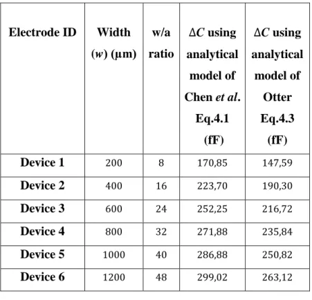
Table 4.1. Capacitance change results ( C) when a DI droplet in silicone oil passes through coplanar electrodes with SiO2 passivation layer. Both analytical
model calculation results are given. The electrode length is equal to microfluidic channel width, 150 µm. The thickness of SiO2 passivation layer
(tP) is 360 nm. Gap (2a) between electrodes is 50 µm. n is taken from 1 to
10000 while calculating Bessel function in Equation 4.3. ... 41
Table 4.2. Capacitance change ( C) results when a DI droplet in silicone oil passes through coplanar electrodes with SiO2 passivation layer. Both analytical
model calculation results are given. The electrode length is equal to microfluidic channel width, 150 µm. The thickness of PDMS passivation layer (tP) is 10 µm. Gap (2a) between electrodes is 50 µm. n is taken from 1 to 10000
while calculating Bessel function in Equation 4.3. ... 41
Table 5.1. Droplet sorting efficiency with respect to droplet speed, droplet size
and electrode type. ... 73
Table 6. 1. Capacitance change results ( C) when a DI droplet in silicone oil passes through PCB electrodes. 100 µm thick glass slide is bonded to microchannels. Devices 1 to 13 are square electrodes and devices 14 to 16 are rectangular electrodes. Capacitance signal amplitudes averaged over 50 droplets for each device. ... 91
Table 6.2. Electric field square gradient results when different configurations of
xviii
Table 6.3. Electric field square gradient results. In PCB DEP electrode Design
1, there are four sharp edges at voltage electrode. In all of these designs, there is only one sharp edge at voltage electrode (Figure 6.12). ... 95
Table 6.4. Electric field square gradient results. PCB DEP electrode Design 2 is
fabricated version of Configuration 15. Electrode length (p) is 800 µm and the distance determines the voltage electrode sharpness (u) is 800 µm for all configurations. ... 96
Table 6.5. Electric field square gradient results calculated through a line in y
direction. The distance between the tip of the voltage electrode and the line is 75 µm. The calculation was done by changing line height in z direction. Figure 6.1 & Figure 6.2 show COMSOL snapshots of these electrodes. ... 97
Table 6.6. Side PCB electrode and our PCB electrode comparison. Electric
field square gradient results calculated through a line that lies in y direction. The distance between the tip of the voltage electrode and the line is 75 µm. The calculation was done by changing line height in z direction. The height of electrodes is 60 µm. Figure 6.3 & Figure 6.4 show COMSOL snapshots of these electrodes. ... 99
Table 6.7. DEP force comparison at different y and z for 60 µm height side
PCB electrodes (Figure 6.3). Electric field square gradient results calculated through a line that lies in y direction. The distance between the tip of the voltage electrode and the line was varied as 65 µm, 75 µm and 500 µm. ... 99
1
Chapter 1
Introduction
Introduction
1.1 Motivation of the Thesis
During the last decades, microfluidic systems became a widespread research area and gave birth to easy-to-use and miniaturized platforms that can be applied to biological and chemical analysis. Microfluidic systems or lab-on-a-chip technologies are of particular interest in this domain owing to the ability of generating, manipulating and processing of small liquid volumes. Due to their miniaturized nature, microfluidic systems especially microdroplet based microfluidic systems provide several advantages such as, enhanced analytical performance with respect to macroscale techniques, low cost and ability to process large libraries of samples in a short amount of time (high-throughput). Nowadays, these platforms are used for deoxyribonucleic acid (DNA) sequencing, chemical and biochemical screening, polymerase chain reaction (PCR), protein crystallization, directed evolution of proteins, detection of rare diseases, cell-cell interactions, single cell analysis etc.
For most of the microdroplet-based systems, one of the fundamental requirements is detection of droplets. Droplet detection has been generally done using optical detection techniques in the literature. Although these systems can detect droplets on the order of kiloHertz (kHz), they are costly and bulky. Also, labeling is needed for detection. On the other hand, electrical sensing provides scalable and label-free alternative for droplet detection, that
2
allows multiple sensors in a small footprint at low cost. Capacitive detection of droplets is a label-free, non-contact detection method. Previously, several groups have demonstrated capacitive sensing [1]–[3]. However, these studies lack the sensitivity that is required for droplet content detection. For this purpose, a droplet content detection system that is scalable, portable and low cost is proposed, designed and fabricated.
Besides droplet content detection, droplet sorting is needed for separating desired material laden microdroplets for further experimentation in microfluidic devices. Dielectrophoresis (DEP) is a commonly used technique for this purpose. Here, DEP systems are investigated using two dimensional (2D) coplanar and three dimensional (3D) eutectic gallium indium (EGaIn) DEP electrodes.
Both droplet content detection and sorting has been accomplished by integrating low cost and portable electronic components with microfluidic devices that have microfabricated electrodes. The fabrication of these conventional electrodes requires costly and time consuming clean room process. In order to decrease the signal to noise ratio and compactness of the system, the use of printed circuit board (PCB) as reusable electrodes has been demonstrated in this thesis. Although dielectrophoretic droplet sorting has been done using various systems, it has never been demonstrated on a printed circuit board. It is shown that PCB based detection and sorting systems would offer portability and scalability when integrated circuits and on PCB electrodes are used.
The finalized integrated system is composed of electrical detection and sorting units that have been completely implemented on a custom designed printed circuit board. The electrodes required for both sensing and actuation of droplets are fabricated using copper traces on printed circuit boards. Placing the microchannels reversibly over the electrodes finalizes the system.
3
An additional benefit of this approach is that the microchannels can be easily replaced while the base platform can be reused for various experiments that can be designed using microdroplets. This integrated system can be reprogrammed for the desired manipulation of droplets. Therefore, this approach provides a versatile microfluidic system.
It is believed that, using off-the-shelf and low cost electrical components can take microdroplet-based microfluidic systems one step further, and turn them into programmable, easy-to-use platforms.
1.2 Overview of Thesis
The thesis continues by reviewing existing microfluidic systems in the literature. In Chapter 3, fabrication and characterization methods are presented. Equipment operation principles are briefly explained. Following Chapter 3, highly sensitive capacitive droplet content detection system is introduced and experimental results are given. In Chapter 5, dielectrophoretic sorting of droplets are presented using 2D coplanar and 3D EGaIn electrodes. On PCB droplet detection is demonstrated and COMSOL simulations are done for finding optimum on PCB DEP electrodes in Chapter 6. The final chapter summarizes the thesis and gives some future outlook.
4
Chapter 2
Scientific Background
Scientific Background
2.1 What is microfluidics ?
Microfluidics is the key science and technology that enables fluid manipulation and control in channels that have dimensions on the order of micrometers. The change in fluid physics in microscale ensures novel usages of microfluidic systems. Although the first microfluidic device was a gas chromatograph invented in 1975, these systems were not used for biological or chemical applications since 1990s [4]. Microfluidic device fabrication technology was derived from microelectromechanical system (MEMS) technology. During the last decades, microfluidic systems became a widespread research area and gave birth to easy-to-use and miniaturized platforms that can be applied to the biological and chemical analysis.
Microfluidics can be divided into three groups as continuous microfluidics, discrete (multi-phase flow or droplet-based) microfluidics and digital microfluidics. Continuous microfluidics is based on continuous liquid flow manipulation. These systems are usually used for simple and well-defined functions such as chemical separation and biochemical applications. Since the surface property of the entire system affects fluid flow at any location in the system, these systems are not suitable for integration and scalability. Discrete microfluidics compartmentalizes and manipulates small volumes of liquid with
5
two immiscible phases. Microdroplets are suitable for very small amount of liquid handling. Since droplet is isolated from its surrounding, any material inside droplet (reagent, cell, protein etc.) is preserved throughout the system. Droplet loading, mixing, sorting, merging, break-up enables high-throughput chemical and biological experimentation due to kHz level droplet generation. Both continuous and discrete microfluidics operates in microchannels. However, digital microfluidics is manipulation of small liquid volumes on open structures using electrowetting method. Electrowetting is changing surface properties of a material by applying electric field. On independently addressed electrodes, small volume of liquids is moved one electrode to another. These systems enable merging of different material loaded droplets. Electrowetting-on-dielectric (EWOD) is common method in digital microfluidics.
Paper-based microfluidic systems are considered as Microfluidics 2.0 by some researchers. This method is inexpensive and easy-to-use. Changing hydrophobicity of the paper at different zones using a printer and wax, channels are fabricated [5]. Printing reagents and other materials to the test zones makes microfluidic paper-based analytical devices (µPADs) cheaper point-of-care-diagnostic devices. Being user-friendly and cheap, paper-based microfluidic systems are developed for disease diagnostics in third world countries [6].
Glass, Si and polymers are three main materials for fabricating microchannels. According to application, any of these three materials can be used. Si wafer is not a suitable material for optical measurement techniques due to its opacity. Glass is a fragile material and etching of it rather difficult than etching a Si wafer. The bonding process requires high voltages or temperatures. Also, a clean-room was needed for the fabrication process [7]. Dimensions of polymers change when they interact with some chemicals such as alcohols. Silicon can be used for applications requiring high temperatures such as quantum dot synthesis [8]. Glass microchannels are resistant to chemicals and reusable. A polymer type, polymethylmethacrylate (PMMA), is suitable for high volume production
6
of cartridges. On the other hand, polydimethylsiloxane (PDMS), is the "working horse" of scientists, since it is non-toxic, opaque material and can be cured at low temperatures. PDMS is a rather cheap material and fabrication of a microfluidic device becomes quite easy with soft lithography techniques.
Microfluidic systems are integrated with different components in order to operate properly. Pumps, valves, mixers, pressure and flow sensors are some of the fluidic components that are used.
2.2 Droplet-based microfluidic systems
Microfluidic systems or lab-on-a-chip technologies generate, manipulate and process small liquid volumes. Due to their miniaturized nature, microfluidic systems especially microdroplet based microfluidic systems provide several advantages such as, enhanced analytical performance with respect to macroscale techniques, low cost and ability to process large libraries of samples in a short amount of time (high-throughput). Nowadays, these platforms are used for DNA sequencing, chemical and biochemical screening, PCR (polymerase chain reaction), protein crystallization, directed evolution of proteins, detection of rare diseases, cell-cell interactions, single cell analysis [9]–[15].
In this section, droplet formation, break-up and merging will be explained and examples from the literature will be given.
2.2.1 Droplet formation
In the literature, there are two main passive droplet formation generators, T-junction and flow-focusing device. Two immiscible fluids are driven from two
7
separate channels and meet a junction that is determined by specific geometry of the channels.
In 2001, Thorsen et al. published an article titled "Dynamic pattern formation in a Vesicle-Generating Microfluidic Device" [16]. For the first time, they accomplished droplet generation with two immiscible fluids using a T-junction. Both water and oil were continuously driven to the microchannel. The water obstructs the main channel at the junction, while oil flows through the channel. At this moment, high shear forces occur. The flow is not linear and static due to interactions between the boundary of two liquids. This instability arises from the competition between surface tension and shear forces. The competition generates droplets. The size and speed of droplets are finely tuned by adjusting water and oil flow rates or pressures.
Anna et al. used flow-focusing technique in a planar microchannel two form droplets [17]. In this technique, two immiscible phases are driven to the one orifice, where the outer channel carries oil and the inner channel carries water. These three channels form a cross at the intersection. The oil comes from two sides of the water and applies pressure to it so that water breaks into droplets. Using this technique, varying size of droplets can be generated at very high speeds.
Three regimes occur during droplet formation depending on physical properties of fluids and external variables. These regimes are categorized as squeezing, dripping and jetting [18]. The physical properties of liquids such as interfacial tensions, viscosities, and external variables as flow rates of fluids, channel dimensions and geometry are used to categorize droplet formations [19]. The dimensionless numbers originated from aforementioned variables determine these regimes. Capillary (Ca) number is the most important dimensionless number for droplet formation and its value varies between 10-3 and 10 (Equation 3.1).
8
(3.1)
In Equation 3.1, µ is the dynamic viscosity of the fluid, V is velocity of the fluid and is interfacial tension between two liquids. Capillary number relates viscous forces with interfacial tension. Abate et al. stated that monodisperse droplets are generated at low capillary numbers for T-junctions and at high capillary numbers for flow-focusing devices [19].
In a T-junction two regimes occur : squeezing and dripping. When dispersed phase (water) completely blocks the main stream channel and there is pressure drop along the droplet due to channel blockage, the regime is called squeezing regime. In dripping regime, droplets do not completely block the main channel and are smaller than the dimension of the main channel. In a flow-focusing device dripping and jetting are two regimes that occur during droplet formation. In dripping regime, the dispersed phase breaks at the moment it enters the junction and turns into droplets. These droplets are immediately carried away by continuous phase. In jetting regime, dispersed phase goes into continuous phase and for a while they co-exist in the main channel [18].
Zeng et al. presents actively controlled droplet formation [20]. In this study, they precisely control droplet formation using a pneumatic PDMS microvalve. This valve controls droplet formation time and size. Abate et al. presents another droplet formation mechanism where they used air bubbles for pinching dispersed phase [21].
9
2.2.3 Droplet Break-up
Droplet break-up provides precisely size controlled daughter droplets from larger droplets. Link et al. demonstrates droplet break up by adjusting microchannel geometry [22]. Passive T-junction and obstacles in the channel are used for studying break-up dynamics. When a droplet flow into a T-junction it breaks itself into two equal sized droplets independent from initial droplet length ratio to the channel width. A T-junction always causes long droplets to break for any flow rate. If a droplet is too small and slowly goes to the junction, it will not break but directs one of the channels. At the bifurcation, droplets break inversely proportional to channel resistances. The channel with higher resistance gets the small portion of the droplet. By making a T-junction tree, it is possible to break larger droplets into 2n daughter droplets, where n is the bifurcation number. Placing a square obstacle in the main channel breaks droplets into varying sizes depending on the obstacle's distance to the walls. An obstacle placed in the middle of the channel creates equal sized droplets, whereas closer side of the obstacle to the channel wall creates smaller droplets. Another study of Link et al. demonstrates droplet break-up in the presence of electric field [23]. Ting et al. studies droplet break-up due to heat. In this study, they use a heater to induce interfacial stress on droplet [24].
2.2.4 Droplet Coalescence
Coalescence of droplets is important in order to provide extended, complex chemical and biological experimentation. Since droplets are little compartments and preserved from the environment, it is not possible to merge content of two droplets in a controllable manner without modifications to the microfluidic system. Bremond et al. states that separation of two droplets favors coalescence [25]. In a diverging-converging channel they accomplish to merge two droplets. When two droplets goes into a diverging channel, they slow down, come closer but do not collide. They collide while first droplet is going through converging
10
channel. Designing an asymmetric chamber is a passive way to merge droplets. Baroud et al. demonstrates that merging of two droplets can be accomplished by lasing the interface of droplets and generating temperature gradient [26]. Also, droplets are prevented from advancing due to laser spot. Surface modification inside microchannel is another droplet merging method [27]. Fidalgo et al. graft hydrophilic polyacrylic acid on PDMS surface that contains benzophenone using photopolymerization method. Hydrophilic region traps droplets so that they merge. One of the passive droplet merging method is to use pillars where first droplet is trapped inside pillars and the second one bumps into it [28]. In this technique, droplet size is important. Applying electric field for merging of droplets is electrocoalescence. Zagnoni et al. demonstrates electrocoalescence with varying electrode shapes and droplet sizes [29]. When a droplet enters to the electrode region, applied electric field causes coalescence. Magnitude of electric field and interdroplet distance are two important parameters to accomplish electrocoalescence.
11
Chapter 3
Fabrication and
Characterization Methods
Fabrication and Characterization
Methods
Electrode, passivation layer and mold fabrication were done in class-100 clean room. For fabrication of substrates underneath microchannels, we benefited from the recipes that was optimized by UNAM clean room engineers. We utilized microchannel mold fabrication and soft lithography knowledge in the group. In this chapter, we give fabrication recipes and briefly explain characterization methods. Soft lithography technique will be introduced and explained.
3.1 Fabrication of Coplanar Electrodes and
Passivation Layer
Before fabrication of the device, both microchannels and coplanar electrodes were designed in a CAD software. Microfluidic device fabrication consists of three steps: patterning of coplanar electrodes on a glass slide, coating of passivation layer onto the electrodes, fabrication of microchannels and bonding. In this section, electrode and passivation layer fabrication will be explained respectively describing photolithography, thin film metallization and dielectric coating. Afterwards, microchannel mold fabrication will be described.
12
3.1.1 Photolithography
Photolithography is the first step of realization of a microstructure. It is for patterning desired geometry to a substrate. In this process, UV (ultraviolet) or optical light is used to transfer the geometry on a mask to a radiation sensitive material, photoresist, that is on the substrate, i.e glass or Si (Silicone) wafer. This process enables micro and even nano sized structures i.e transistors, photodiodes, membranes, electrodes to be fabricated. There are two types of photoresists as positive and negative. In developer solution, UV radiated part and non-radiated part of positive and negative photoresist dissolves, respectively. Generally, photomasks are used for the cases where higher resolution is needed. For fabrication of photomasks, generally chrome deposited and resist coated glass substrates are used and desired structures are written on it using a mask writer or e-beam lithography. Eventhough using a photomask is good for obtaining higher resolution, transparency mask is better choice for resolutions equal or higher than 20 µm since it is cheap. Using a high DPI (dot-per-inch) printer and an acetate film, it is possible to transfer software design to this film. In our case, for fabrication of electrodes we used transparency masks and 1 mm glass slides as substrate. Photolithography recipe for fabricating coplanar electrodes is,
Design coplanar electrodes using a CAD software.
Use a high dpi printer to print the mask designs on an acetate film. The more dpi of the printer, the more resolution you can get. Tape this film on a 4 inch square glass to obtain your mask.
Clean glass substrate with acetone, IPA and DI water respectively. Dry with nitrogen. Bake it on a 110 hot plate on 5 - 10 minutes. This is dehdyration bake.
13
Spin coat HMDS (hexamethyldisilazane) on the glass 4000 rpm for 40 seconds. HMDS increases adhesion of photoresist to the substrate. On top of HMDS, spin coat AZ5214 positive photoresist at 4000 rpm
for 40 seconds.
Bake substrate for 50 seconds at 110 hot plate.
Expose photoresist coated glass substrate to 365 nm UV light with dose of 50 mJ/cm2 (EVG620).
Put glass substrate into AZ400K developer : DI water (1:4 v/v) mixture for 30 seconds in order to dissolve UV radiated regions.
Control the sharpness of developed regions using a microscope.
3.1.2 Thin film metallization
Coplanar electrodes on a 1 mm thick glass slide was fabricated using metal deposition technique. After photolithography, one of the physical vapor deposition methods (sputtering, thermal evaporator) was used to deposit metal on photoresist coated substrates. Cr/Cu pair is used to fabricate coplanar electrodes. Cr easily sticks to the glass substrate, therefore forms adhesive layer for Cu. Following metallization, lift-off is done by immersing metal coated substrates into acetone. Acetone removes photoresist, so regions without photoresist that was defined by photomask determine the structure after lift-off. In order to remove the photoresist, ultrasonic agitator can be used for short period of time.
3.1.2.1 Sputtering
Sputtering is one of the physical vapor deposition methods. Using sputtering, insulating or conductive thin films can be fabricated. For conductive coatings like in our case, DC magnetron sputtering is used (Vaksis, NanoD-4S). Sputtering chamber operates at room temperature. Substrate is rotated for
14
uniform film thickness. Under optimum chamber pressure, Ar gas flows into the chamber. Highly energized Ar ions physically bombard targets (coating materials, Cr and Cu consecutively) and break-off atoms from the target material under plasma. These atoms move towards the substrate and coat the substrate surface. The recipe for 220 nm Cr/Cu coplanar electrodes is given in Table 3.1.
Table 3.1. Sputtering process parameters for 220 nm Cr/Cu deposition
Parameters 20 nm Cr
coating
200 nm Cu coating
DC power 150 W 150 W
Argon gas flow 70 sccm 50 sccm Chamber pressure 8 mTorr 20 mTorr
Time 2 min 8 min
3.1.2.2. Thermal Evaporator
Thermal evaporator is another physical vapor deposition method. This deposition method relies on melting of coating materials at temperatures until 1500 . Cr and Cu pellets are placed on tungsten boots. Passing through tungsten boots, after some time current leads to temperature increase on boots resulting in melting of the coating material. Depending on the material and thickness of the tungsten boot, the applied current is changed. The vapor of the melted material moves toward the substrate and coats it. The rate of evaporation is important while coating the substrate. It should be observed during the process to adjust it properly. Substrate rotation is used for uniform film thickness. In our case, first Cr then Cu is coated. Since the melting point of Cr is higher than Cu, higher current (100 A) was used for melting Cr.
15
3.1.3 Dielectric film coating
Dielectric film coating on coplanar electrodes is needed as passivation layer to prevent droplet pinning onto the electrodes and contamination between consecutive droplets. For droplet and droplet content sensing applications, thinner passivation layer between microchannels and coplanar electrodes enhances the capacitance signal amplitude, therefore, increases the resolution of the system.
3.1.3.1 Plasma Enhanced Chemical Vapor Deposition
(PECVD)
PECVD is a method for coating dielectric films. Unlike other chemical vapor deposition techniques, PECVD operates at low temperature (200 - 400 ). It is a good candidate for applications where high temperature damages the device. While reactant gases flow through between ground and energized RF electrodes, capacitive coupling of electrodes initiates plasma. The resulting chemical reaction yields solid film on the substrate. The substrate is placed onto the ground electrode that is heated. For fabrication of devices, SiO2 (silicon
dioxide) is used as passivation layer between microchannels and coplanar electrodes. SiH4 (silane) and N2O gases were used to form plasma at 200 .
SiH4 and N2O reacts to form solid SiO2, N2 and H2 gases. He gas were used to
slow the reaction. Target pressure and RF power were set as 1 Torr and 10 W. Thin film thickness is adjusted by changing process time.
3.2 Fabrication of Microchannel Mold
Microchannels were fabricated by taking replica of channel mold that is on a SU-8 coated Si wafer using PDMS (polydimethlysiloxane). For fabrication of microchannel molds two types of negative photoresist , SU-8 2005 and SU-8 2050, were used by applying photolithography techniques. During this process,
16
transparency mask was used. SU-8 2005 and 2050 were spin coated on Si wafer respectively. Dispensing SU-8 2005 beneath SU-8 2050 prevents the stiction of PDMS on silicon wafer and enables easy removal of cured PDMS from the mold since PDMS sticks to Si, but not SU-8. Generally, instead of spinning thin SU-8 2005 beneath SU-8 2050, researchers apply silanization process before PDMS molding to make Si surface hydrophobic. At the end of the process, SU-8 developer was used for extracting the mold structure. Process flow is given in Figure 3.1. For 80 µm height mold, detailed process is given below:
Design microchannels using a CAD software.
Use a high dpi printer to print the mask designs on an acetate film. The Tape this film on a 4 inch square glass to obtain your mask.
Clean the 4 inch Si wafer with acetone, IPA and DI water respectively. Dry with nitrogen. Bake the wafer on a 120 hot plate on 5 - 10 minutes. This is dehdyration bake.
Cool it to room temperature.
Spin coat SU-8 2005 using the following parameters :
Time 25 sec 40 sec
Speed 500 rpm 2500 rpm
Acceleration 100 rpm/s 200 rpm/s
This is a two step spinning process. The first step provides dispersion of the SU-8 to the whole surface of the Si wafer.
After spinning SU-8 2005, bake it using a three step baking process on a hot plate. This is a gradual process to prevent film from forming cracks. This is soft baking.
65oC 2 min 95oC 4 min 65oC 1 min
17
Cool the wafer down to room temperature.
Expose the baked Si wafer with 120 mJ /cm 2 UV light at 365 nm without using a mask. This is exposure.
Bake it on hot plate using a gradual process. This is post exposure bake. 65oC 1 min
95oC 3 min 65oC 1 min Cool it to room temperature.
Spin coat SU-8 2050 using the following parameters :
Time 45 sec 35 sec
Speed 500 rpm 2000 rpm Acceleration 50 rpm/s 300 rpm/s
After coating process is finished, take the excess SU-8 2050 from the edges of the wafer using a glass slide. This is edge bead removal.
Bake it on hot plate using a gradual process.
Cool it down to room temperature.
Expose the baked Si wafer with 230 mJ /cm 2 UV light at 365 nm using acetate film taped 4 inch glass (mask).
Bake it on hot plate using a gradual process. 65oC 4 min 95oC 8 min 65oC 2 min
18 Cool it down to room temperature.
Pour SU-8 developer solution into a glass container. Put your wafer into the solution for 6 minutes. Depending on the freshness of the developer solution this time may decrease or increase. Therefore, observe it during the process.
Dry it with nitrogen. Never use water in this step. Control the microstructures under a microscope.
In order to prevent delamination of SU-8 layers during PDMS replica molding, apply epoxy to the edges of the wafer and kept it at room temperature overnight. After epoxy is dried, apply baby powder to the epoxy applied regions prevent stiction of PDMS.
65oC 3 min 95oC 8 min 65oC 1 min
19
Figure 3.1. Schematic of mold fabrication using SU-8 negative photoresist
3.3 Soft Lithography
Soft lithography is a method that refers replicating mold structure using polymeric, "soft", materials by stamping. For fabrication of microchannels,
20
PDMS (polydimethylsiloxane) is used as soft material. Soft lithography steps are written below :
Pour 10:1 (w/w) ratio Dow Corning Sylgard 184 silicone elastomer and silicone elastomer curing agent into a plastic cup. First pour 30 g silicone elastomer , then 3 g curing agent. Since curing agent amount is less, be careful while pouring it.
Using a plastic spoon, mix them. Let silicone elastomer absorb curing agent. Do this with using spoon and don't daub it to the sidewalls of the cup. While mixing, a lot of air bubbles will be generated. Try to increase amount of air bubbles. Until all mixture is composed of air bubbles continue to mix.
Remove plastic spoon. Put the mixture into a dessicator. The air inside the dessicator will be removed by pump. While the pressure inside the chamber is decreasing, the bubbles expand. When lid of the dessicator is opened, due to increasing pressure bubbles will explode. Continue this process until all the bubbles explode and the mixture become transparent. The bubbles explode when the mixture is left in a room for some time. However, this process takes too much time that while bubbles are exploding, curing occurs. It is wise to use a dessicator. Use VWR aluminum pans that a 4 inch wafer fit into. Raise sidewalls of
the aluminum pan to prevent leakage of PDMS. Put mold into it. Dispense transparent PDMS mixture from the center of the mold at a low altitude. During this process, prevent air trapping inside PDMS. Pouring PDMS mixture from high altitude causes air trapping. After dispensing all the mixture inside the cap, using a needle pop the air bubbles in the mixture. If these bubbles are close to your channel, they will damage the structure of the channel. Also, for better view under microscope try to pop all the bubbles.
Put aluminum pan on a 100 hot plate for 4 hrs to cure PDMS. In about 30 minutes, the PDMS becomes solid. Be sure that hot plate is flat. An uneven hot plate causes non uniform distribution of liquid
21
PDMS. Therefore, precision tips are not stay in inlets where the thickness of the PDMS slab is too thin.
After 4 hours, take the solid PDMS from the hot plate. Lay stretch film on a flat surface. Be sure that stretch film is not too tight. Remove mold containing PDMS from the aluminum pan. Put upper side of the PDMS slab onto stretch film. Using a scalpel, cut excess PDMS around the mold.
Lay another layer of stretch film on a flat surface. By putting your fingernail between PDMS and mold, try to release PDMS from the mold at the borders of the mold. After releasing the PDMS along the mold contour, using your hand release the PDMS from the mold. Put it onto stretch film.
Using a scalpel divide the PDMS slab into separate sections that contain microchannels.
Punch inlet and outlet using a biopsy punch. These holes provide connection between microchannel and liquids. While using biopsy punch be sure that stretch film on both sides of the inlet is slightly removed.
This PDMS slab only contains three walls of the microchannel. By bonding PDMS to glass or PDMS provides four walled microchannels. Bonding can be done using air or oxygen plasma. Plasma treatment converts naturally hydrophobic PDMS surface into hydrophilic one, so it is possible to use water inside microchannels. Therefore, after plasma treatment dangling bonds occur on the surface of both materials. When two surfaces come together, they form unbreakable bonds. This is bonding of PDMS to glass slide. For PDMS glass bonding the following recipe can be used :
Clean glass slide using acetone, IPA and DI water.
22
Put PDMS slab into a plasma cleaner (Nanoplas, DSB6000) chamber where microchannel is at upward position. Also, put glass slide into chamber.
Apply oxygen plasma for 1 min., 30 sccm O2 flow rate at 50 W.
Quickly get treated surface of PDMS and glass slide together.
Immediately after bonding, bake bonded device on 100 hot plate for 12 hours for enhancement of the bonding.
For PDMS-PDMS bonding parameters are, 30 W, 30 sec, 56 sccm O2 flow rate.
3.4 Characterization Methods
Characteristics of fabricated devices were measured using different apparatus. After every fabrication process, i.e., fabrication of coplanar electrodes, mold, spin coating of PDMS on coplanar electrodes, characterization step was completed. Thickness of coplanar electrodes on glass slides, spin coated PDMS layer and deposited SiO2 on coplanar electrodes, mold height were measured
using Atomic Force Microscopy (AFM) (PSIA, XE-100E, Suwon) , Variable Angle Spectroscopic Ellipsometer (J.A. Woollam, V-VASE) and Stylus Profilometer (KLA Tencor, P6 Surface Profiler). During the experiments, microfluidic devices were tested using a pressure pump. In this part, characterization methods that are used during the studies will be explained briefly.
3.4.1 Atomic Force Microscopy (AFM)
Binnig, Quate and Gerber invented Atomic Force Microscope in 1986 [30]. Atomic force microscope combines properties of a surface profilometer and a scanning tunneling microscope. Unlike scanning tunneling microscope, atomic force microscope can be used on both conductive and insulating surfaces. It is a powerful microscopy technique, since it is possible to measure angstrom scale surface thickness with it. The AFM operation principle as follows: AFM
23
cantilever is brought close to the sample to scan the surface, so attractive force occurs between the surface and the cantilever tip. This force leads cantilever to deflect towards the sample surface. After some proximity, i.e tip contacts with the surface, the force becomes repulsive, so the cantilever tip deflects away the surface. A laser beam is reflected from the flat top of the cantilever while it is operating through a surface. This information is collected by position sensitive photodiode and turned into a surface topography image with software.
The mostly used operation modes of an AFM are contact, noncontact, and tapping mode. Contact mode is static and the other two modes are dynamic modes. The difference between tapping and noncontact mode is that, in tapping mode cantilever tip touches to the surface, but in noncontact mode cantilever tip is close to the surface throughout the measurement.
For measuring coplanar electrode thickness, AFM (PSIA, XE-100E, Suwon) is used with tapping (intermittent contact) mode in air under ambient temperature . A Tap190Al-G probe with a force constant of approximately 48 N/m and resonance frequency of 190 kHz was used.
3.4.2 Variable Angle Spectroscopic Ellipsometer
Ellipsometry is an optical technique that measures the polarization change of the reflected light beam from the surface. It is non-destructive and requires neither sample preparation nor special environment. When the incident beam reflected from the surface and the substrate beneath the surface, it experiences polarization change that is specific to structure of the surface. Using polarization change data, various information can be extracted; film thickness, refractive index (n), extinction coefficient (k), surface roughness and anisotropy of grown materials by fitting the experimental data to a theoretical model. Ellipsometry is capable of measuring film thicknesses from several angstroms to micrometers.
24
Thickness of the SiO2, PDMS and toluene-thinned PDMS passivation layers
were measured using an Ellipsometer (J.A. Woollam, V-VASE). Ellipsometer was used at an incidence angle of 65o. Cauchy dispersion function was used to determine passivation layer thicknesses. The refractive indices of PDMS and toluene-thinned PDMS are the same, since toluene evaporates during and after spin coating, leaving only PDMS as a passivation layer. In that regard, toluene is only used to decrease the viscosity of the PDMS mixture before spinning, in order to decrease passivation layer thickness. In order to fit experimental data, refractive indices of PDMS and toluene-thinned PDMS were taken as 1.42, and refractive index of SiO2 was taken as 1.55.
3.4.3 Stylus Profilometer
Profilometer is a surface thickness and roughness measurement apparatus. A diamond stylus contacts with the surface of the sample and goes along the surface for a specified distance. Depending on stylus diameter and the contact force of the stylus, it can measure various thicknesses from nanometer to millimeter. Scan rate and signal sampling rate controls horizontal resolution. The software converts analog stylus vertical position into digital data.
In order to characterize microchannel heights, molds were measured using a stylus profilometer (KLA Tencor, P6 Surface Profiler). Also, spin coated PDMS membrane thicknesses for on PCB droplet detection and sorting experiments were measured.
25
Chapter 4
Droplet content detection
using integrated capacitive sensors
Droplet content
detection using
integrated capacitive sensors
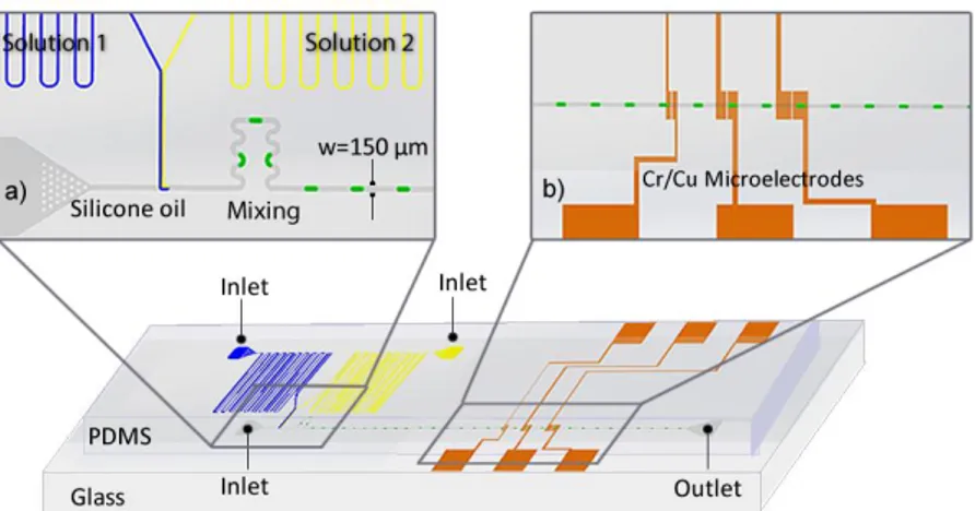
This chapter is based in part on the publication “Microfluidic droplet content detection using integrated capacitive sensors,” P. K. Isgor, M. Marcali, M. Keser, and C. Elbuken, Sensors and Actuators B : Chemical, (2015).
4.1 Introduction
Detecting analytical content of droplets is one of the fundamental requirements for most of the microdroplet based systems. Electrical droplet sensing provides a scalable and label free alternative for the more prevalent optical detection techniques, which allows multiple sensors in a small footprint at very low cost. Although, optical systems can detect droplets at very high rates (on the order of kHz), these systems are not scalable [31]. Microfluidic capacitive sensors have been used for detection of droplets, however they have been lacking the sensitivity required for detecting the content of droplets. The previous studies that utilize off-the-shelf electronic components fall short in providing the sensitivity that is required for droplet content detection [32], [2] . For instance, Demori et al. have reported capacitive detection of liquids due to different dielectric properties. They have used a custom-made electronic circuitry for
26
liquid detection and reported the resolution of their system as 0.06 fF. However, the resolution of the system is a function of sensor geometry, which determines the absolute value of the capacitance value measured. A better metric for this study is the resolution in terms of the dielectric constant unit. When the study is analyzed in depth, their dielectric constant resolution is found 5.5 dielectric units. Moreover, these measurements were performed in a continuous flow regime. Thus, there is need for off-the-shelf detection systems that provide high sensitivity for droplet content detection. In order to fill this gap, we demonstrated capacitive droplet content detection using commercially available sensors.
We developed a scalable, portable, and highly sensitive capacitive microdroplet content detection system using coplanar electrodes with nanometer thick silicon dioxide (SiO2) passivation layer and commercially available, low-cost
capacitive sensors and a microprocessor. For this purpose, we designed a Y-junction microfluidic device that allows modification of droplet content by mixing ethanol and distilled (DI) water at any ratio. When a droplet enters the sensing region where coplanar electrodes are placed, the change in dielectric permittivity leads to the change in capacitive signal. Moreover, changing droplet content changes capacitive signal amplitude. We characterized the system by modifying the dielectric content of the droplets on the run and measuring the corresponding capacitance signal. We calculated the system resolution as 3 dielectric permittivity units. We verified the results using a semiconductor parameter analyzer. We enhanced the signal by minimizing the thickness of the passivation layer. The application specific integrated circuit used in this work enables a portable, low-cost detection system and matches the performance of bench-top analyzers. To the best of our knowledge, we achieved the most sensitive capacitive detection signal in the literature. This system can be used for very precise droplet size and speed detection as well as droplet counting.
27
We believe that using off-the-shelf and low cost electrical components for high sensitivity droplet content can take microdroplet-based microfluidic systems one step further, and turn them into programmable and easy-to-use platforms. This study takes a step in that direction by utilizing very low cost electronics (in total $24) for high sensitivity droplet content measurement.
4.2 Capacitive detection theory
In a droplet based microfluidic system that includes coplanar electrodes beneath microchannel, DI water droplets in silicone oil lead to capacitance value change when droplets enter sensing region due to stark contrast between dielectric permittivity of silicone oil (Ɛr = 2.5) and water (Ɛr_water = 80). In order to
calculate the capacitance formed by coplanar electrodes under changing medium, there are two theoretical models in the literature. Chen et al. calculated capacitance using conformal mapping with an inverse-cosine transform, and Otter used Fourier series approximation of surface potential [33], [34]. In this part, these two models will be briefly explained. The models are used for calculating capacitance change value for a DI droplet in silicone oil.
Chen et al. have computed capacitance of parallel coplanar electrodes. They studied a system which has a single dielectric layer on top of planar electrodes, as shown in Figure 4.1 [33]. An electrical potential difference was applied to the electrodes and electric field distribution was solved using conformal mapping techniques. The authors concluded with the following formula (Equation 4.1) for the calculation of capacitance formed by fringing fields
ε ε (4.1) where w is the width of the electrode, L is the overlapping length of the electrodes (L w), a is the half gap between the electrodes, εr is the
28
permittivity of the dielectric layer and εo is the dielectric permittivity of the
vacuum. This equation gives very good results for electrode designs satisfying
w/a 1 and close approximation for w~a [33].
Figure 4.1. Schematic of the system studied by Chen et al. [33]
Another analytical model was suggested by Otter, where approximate surface potential was used in order to simplify Engan’s equation [34], [35]. For an interdigitated electrode, as shown in Figure 4.2, an approximate capacitance expression was computed [34]. In this model, the potential around the electrode was described using Fourier series, since interdigitated electrodes have a periodicity and fringing fields at the electrode periphery was neglected. The capacitance of the interdigitated electrode was found as
ε ε
(4.2)
where p is the length of the overlap of the electrodes, q is the total width of the interdigitated electrode, s is the gap between electrodes, a=s+w is the periodicity and J0 is the zeroth order Bessel function. In this model, the
thickness of the electrodes was neglected as compared to the system’s other dimensions and number of electrodes was assumed to be large. Moreover, the width and gap between electrodes were taken as uniform. Also, p was assumed to be much larger than w and s.
29
As seen from Equation 4.1 and Equation 4.2, the two models for the calculation of capacitance by coplanar electrodes look quite different. For the ease of comparison, it is wise to use the same notation for these two models. Therefore, Equation 4.2 was rewritten by using variables consistent with Equation 4.1 as
ε ε
(4.3)
where a is the half gap between electrodes, w is the width of the electrodes, L is the overlapping electrode length, N is the number of electrodes which was found by dividing q by a.
Figure 4.2. Schematic of the system studied by Otter [34].
Electrode width and gap determines the penetration depth of electric field lines. Some of field lines go through the PDMS bulk as shown in Figure 4.3.a. Owing to lower dielectric permittivity than the channel, the contribution of bulk PDMS to the capacitance signal is negligible. Therefore, only a portion, effective width, of the electrode is responsible for the signal detected by the sensor [33]. Using FEM simulations, Sun et al. have shown that for a fixed channel height and electrode gap, increasing electrode width does not excessively change electric field magnitude [36]. As a result, the capacitance formed by (w-weff)