XXX-X-XXXX-XXXX-X/XX/$XX.00 ©20XX IEEE
Mic-in-CMOS:
CMUT as a Sealed-Gap Capacitive Microphone
Hayrettin Koymen Nanofone Ltd. Guilford, UK ORCID: 0000-0002-9768-2110 Itır Köymen EEE Department TOBB University of Economics andTechnology Ankara, Turkey ORCID: 0000-0002-7233-2704 Yavuz Ahiska Nanofone Ltd. Guilford, UK [email protected] A. Sinan Tasdelen BASTA Bilkent University Ankara, Turkey [email protected] Abdullah Atalar EEE Department Bilkent University Ankara, Turkey ORCID: 0000-0002-1903-1240 Mehmet Yilmaz UNAM Bilkent University Ankara, Turkey [email protected]
Abstract— The design and production of a CMOS compatible, watertight and ingress-proof CMUT (capacitive micromachined ultrasonic transducer) microphone, mic-in-CMOS, with vacuum-gap is described. We present an analytical model-based approach for the design of mic-in-CMOS, where a basis for quantitative comparison of performance trade-offs is provided. The sealed vacuum gap of the mic-in-CMOS is basically a lossless sensor, free of mechanical noise. Its SNR is determined by the noise of the pre-amplification electronics (the noise contributor in a CMUT with vacuum gap is essentially the radiation resistance, which is less than 0 dBA for audio band for a 1 mm2 device). The design of mic-in-CMOS involves many
multilateral trade-offs such as gap height vs membrane thickness vs sensitivity vs need for linear operation vs bias voltage and atmospheric depression, to name few. The mic-in-CMOS design can be mass produced using mic-in-CMOS film stacks only, as such the fabrication process can be carried out entirely in a CMOS processes production line complemented with CMOS compatible post-processing approaches. Mic-in-CMOS has the advantage of low production cost with minimal packaging requirement and on-die EMI / EMC.
Keywords—Capacitive microphone. Sealed gap, MEMS, CMUT, CMOS
I. INTRODUCTION
The state-of-the-art capacitive MEMS Microphones incorporate very compliant (perforated silicon) membranes and pressure compensated gap. These membranes resonate at 25−30 kHz, slightly over the audio frequency band. The sensor noise level is about 27−30 dBA, which is dominated by the air friction at the perforations of the membrane. The sensitivity achieved at this noise level is such that the required biasing and pre-amplification electronics can be designed with the same level of noise contribution.
The noise contributor in a CMUT with vacuum gap is essentially the radiation resistance, which is less than 0 dBA for audio band for a 1 mm device. Also, such a CMUT is waterproof since the gap is sealed. The sensitivity of this microphone is lower due to less compliant membrane, because there is a need for maintaining an elastically linear operation under atmospheric pressure. The SNR is determined by the noise of the pre-amplification electronics.
In this paper, an analytical model-based approach for the design of these microphones is presented [1]. An analytical basis is provided for quantitative comparison of performance trade-offs. The three critical dimensions: the gap radius, the effective gap height and the membrane thickness are determined uniquely for a given performance.
This design method exploits the standard CMOS materials and process thicknesses to construct a microphone in CMOS,
mic-in-CMOS. This production process requires some extra
post processing steps. CMOS processes have been utilized to produce sealed gap CMUT devices by post-processing fabricated CMOS chips [2-8]. In such studies, depending on the design, metal, alloy, polysilicon, or SiO layers are designated as sacrificial layers. Similarly, SiO , metal, alloy or polysilicon films could be used as structural layers. Once the sacrificial layers are etched from the CMOS chip, the microphone gap entrances/exits are sealed under low pressure. The gaps can be sealed with thin films of either SiO or Si N , or conformal coating materials according to the design needs.
It is important to note that through the design method employed in this work, the mic-in-CMOS is fabricated on the same die as the pre-amplification and other electronic stages.
II. DESIGN THEORY
In the presented method, it is shown that the performance of sealed vacuum gap capacitive microphones can be expressed using only three independent parameters [1]: (i)
: dc bias voltage; (ii) ⁄ (<1): The ratio of ambient pressure to the pressure necessary to depress the microphone plate by effective gap height; (iii) ⁄ (<1): the ratio of the dc bias voltage to the collapse voltage at the ambient pressure. All of the properties of the microphone, including performance related ones like sensitivity (open circuit received voltage or short circuit received current) and the input impedance are uniquely specified once these three parameters are specified. The dimensions of the microphone, depicted in Fig.1, are also determined using only these three parameters and the plate material properties.
A. Gap and plate dimensions
The device is analytically described in terms of variables such as dimensions and relevant voltage values in detail in [1]. To summarize the main points, the effective gap height is expressed as:
Fig. 1. Cross sectional view of the circular mic-in-CMOS geometry. Top electrode is placed on the bottom of the microphone plate and the insulating dielectric layer is on the bottom electrode.
= + ⁄ (1) where is the physical gap height, is insulator thickness and is the relative permittivity of the insulating layer, can be expressed as:
= _ _
(2) where is the collapse voltage,
_ =
(3) is the reference voltage (collapse voltage in vacuum), and
VDC_n is related to the bias voltage as expressed in:
_ =
3 2
(4) which is 1.4 × 10 ( ) for a vacuum sealed gap at Standard Atmospheric Pressure (SAP). and are ambient static pressure and permittivity of free space. The normalized effective gap height, _ , depends only on
Fb/Fg, since as described in [9]. This can be expressed as:
V V ≈ 0.9961-1.0468 F F + 0.06972 F F -0.25 + 0.01148 F F (5)
The optimum effective gap height is uniquely determined by the bias voltage and the atmospheric depression and it is independent of plate material properties.
For a given set of operational parameters, ( , ⁄ , ⁄ ), there is a minimum value for the microphone radius. This minimum value can be expressed as follows:
(a)
(b) _
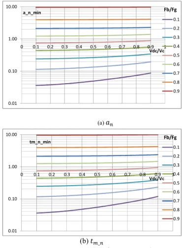
Fig. 2. Normalized dimensions an and _ versus ⁄ for different values of ⁄
= 10
15(1 − ) _
(6)
where is the ambient static pressure, and are the Young’s modulus and Poisson’s ratio of the plate material, respectively, and normalized radius, , is given as:
=
_
/ (7)
For a silicon plate, the material dependent term is found as: 10
15(1 − ) = 178
(8) when is equal to SAP. If the plate is made of few layers of different materials, equivalent and are employed in the calculation [10]. The plate is a composite of aluminum and oxide layers if fabricated in CMOS processes, in which case this term becomes 150. This normalization parameter for the radius is non-dimensional and contains only the elastic constants of the plate material and the differential static pressure.
The normalized radius, , is independent of material properties and the bias voltage, but it is a function of only the
0.01 0.10 1.00 10.00 0 0.1 0.2 0.3 0.4 0.5 0.6 0.7 0.8 0.9 1 a_n_min Vdc/Vc Fb/Fg 0.1 0.2 0.3 0.4 0.5 0.6 0.7 0.8 0.9 0.01 0.10 1.00 10.00 0 0.1 0.2 0.3 0.4 0.5 0.6 0.7 0.8 0.9 1 tm_n_min Vdc/Vc Fb/Fg 0.1 0.2 0.3 0.4 0.5 0.6 0.7 0.8 0.9
operational parameters ⁄ , and ⁄ . In order that the microphone plate remains elastically linear, its radius-to-thickness ratio must be less than a maximum, ( ⁄ )_
[1]. This limit is also a function of same operational parameters. The variation of with respect to ⁄ and
⁄ depicted in 2(a).
(a)
(b) a
(c)
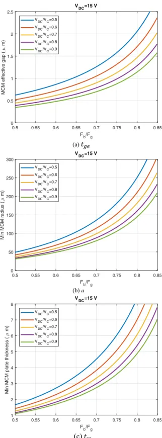
Fig. 2. The gap height, radius and the thickness of a silicon membrane designed for 15 V bias as a function of ⁄ and ⁄
The plate thickness for this radius is similarly obtained as [1], _ = 5 _ _ (9) where; _ = _ (10) The variation of _ with respect to ⁄ and ⁄ is
depicted in 2(b).
B. Scaling
It is possible to increase the microphone gap radius beyond such that same performance is maintained at the same effective gap height and operating parameters ( , ⁄ , ⁄ ). The new radius and the plate thickness are determined as:
= (11)
and
= _ (12)
where K>1. This property is referred to as scaling.
C. Microphone design for 15V bias
The variation of the dimensions of a silicon microphone, designed for 15 V bias, with respect to atmospheric depression is depicted in Fig. 2(a) for various values of
⁄ . For example, if the microphone is intended to be used at ⁄ =0.7 and ⁄ =0.7, the effective gap height must be set at = 0.90 µm.
The radius and the membrane thickness for this bias voltage is also given in Fig. 2 when the membrane is made of silicon. The thickness is =3.2 µm and radius is =100 µm. The radius also depends on the plate material properties but this dependence is rather weak. The radius varies by the fourth root of the material stiffness so that, for example, if silicon oxide plate is used instead of silicon, a minimum radius of 83 µm is necessary instead of 100 µm, although the Young’s modulus of silicon is more than twice as large as that of silicon oxide. The effective gap height and the thickness remains the same.
The approach presented in this paper can also be extended to cover elliptic gaps and plates and convex polygons and elliptic polygons [11]. Same methodology is applicable to square and rectangular microphones, although circular geometry is always more sensitive for a given area.
The required gap heights and plate thicknesses are suitable for designing microphones to be fabricated in standard CMOS fabrication processes. The octagonal gaps and plates are particularly convenient for this purpose.
Sealed gap microphone open-circuit-receive-voltage (OCRV) sensitivity is significantly less compared to MEMS microphones with pressure compensated gap. This is because of the need for relatively thick plates. For example, radius-to-thickness ratio for silicon plates must be less than 35 in order to maintain elastically linear operation under SAP. The lower 0.5 0.55 0.6 0.65 0.7 0.75 0.8 0.85 Fb/Fg 0 0.5 1 1.5 2 2.5 MCM effective gap ( m) VDC=15 V V DC/VC=0.5 V DC/VC=0.6 V DC/VC=0.7 V DC/VC=0.8 V DC/VC=0.9 0.5 0.55 0.6 0.65 0.7 0.75 0.8 0.85 Fb/Fg 0 50 100 150 200 250 300 Min MCM radius ( m) VDC=15 V V DC/VC=0.5 V DC/VC=0.6 V DC/VC=0.7 V DC/VC=0.8 V DC/VC=0.9 0.5 0.55 0.6 0.65 0.7 0.75 0.8 0.85 Fb/Fg 1 2 3 4 5 6 7 8
Min MCM plate thickness (
m) VDC=15 V V DC/VC=0.5 V DC/VC=0.6 V DC/VC=0.7 V DC/VC=0.8 V DC/VC=0.9
microphone output voltage places more demand on low noise pre-amplification. Nevertheless, when the microphone is implemented in a CMOS process integrated with the preamplifier, it was possible to obtain 62 dB SNR.
III. INTEGRATED ELECTRONICS
The amplifying electronics is a simple nMOS common source stage with a resistive load, providing a voltage gain of about 10. To reduce the noise of the stage, the gate bias resistance should be very large. To realize a large resistance we use two transistors, one nMOS and the other pMOS both with a gate to source voltage below the threshold voltage. To have a low noise transistor, the amplifying transistor should normally be chosen with a W/L ratio as large as possible. The input gate capacitance of the transistor will generate a voltage divider, reducing the effective input voltage since our input source is purely capacitive. Consequently, there is an optimum value of W/L ratio that gives the highest output signal-to-noise ratio.
IV. POST PROCESSING
After the CMOS processing of a wafer is completed using standard approaches, post-processing of the mics-in-CMOS is initiated and completed using mics-in-CMOS compatible, wafer-scale adaptable, and batch-compatible unit processes and integration processes. The mic-in-CMOS devices are suitable for mass production using "CMOS film stack only", entire in-CMOS processes production line and CMOS compatible post-processing approaches.
"CMOS compatible post-processing approaches" are composed of etching and deposition steps that may need one or at most two simple (i.e. not technology challenging) lithography levels for the formation of a sealed vacuum gap microphone that becomes watertight and ingress-proof".
V. CONCLUSION
Mic-in-CMOS, a sealed gap microphone, which is suitable for production in CMOS manufacturing processes is presented in this paper. The analysis and design methodology is fully disclosed. It is possible to get optimum designs for
different CMOS manufacturing processes using this approach. The preamplifier and other sensor electronics is readily integrated on the same CMOS die. Presented results are applicable to variety of gap geometries.
REFERENCES
[1] US Patent US20180302726 - HIGH PERFORMANCE SEALED-GAP CAPACITIVE MICROPHONE, granted: 07.05.2019.
[2] P.-C. Eccardt, K. Niederer, T. Scheiter, C. Hierold, "Surface micromachined ultrasound transducers in CMOS technology," in 1996 IEEE Ultrasonics Symposium. Proceedings, San Antonio, 1996. [3] P.-C. Eccardt, K. Niederer, “Micromachined ultrasound transducers
with improved coupling factors from a CMOS compatible process”, Ultrasonics, volume 38, p. 774–780, 2000.
[4] Po-Kai Tang, Po-Hsun Wang, Meng-Lin Li, Michael S.-C. Lu, “Design and Characterization of the Immersion-Type Capacitive Ultrasonic Sensors Fabricated in a CMOS Process”, Procedia Engineering Volume 5, 2010, Pages 669-672, Proc. Eurosensors XXIV, September 5-8, 2010, Linz, Austria.
[5] Christopher B. Doody, Xiaoyang Cheng, Collin A. Rich, David F. Lemmerhirt, Robert D. White, «Modeling and Characterization of CMOS-Fabricated Capacitive Micromachined Ultrasound Transducers,» Journal of Microelectromechanical Systems, volume 20, no. 1, pp. 104-118, 2011.
[6] Meng-Lin Li, Po-Hsun Wang, Pei-Liang Liao, Michael S.-C. Lu, “Three-Dimensional Photoacoustic Imaging by a CMOS Micromachined Capacitive Ultrasonic Sensor”, IEEE Electron Device Letters, volume 32, no. 8, pp. 1149-1151, 2011.
[7] Po-Kai Tang, Po-Hsun Wang, Meng-Lin Li, Michael S-C Lu, “Design and characterization of the immersion-type capacitive ultrasonic sensors fabricated in a CMOS process”, Journal of Micromechanics and Microengineering, Volume 21, Issue 2, article id. 025013, 8 pp. (2011).
[8] David F. Lemmerhirt, Xiaoyang Cheng, Robert D. White, Collin A. Rich, Man Zhang, J. Brian Fowlkes, Oliver D. Kripfgans, “A 32 × 32 Capacitive Micromachined Ultrasonic Transducer Array Manufactured in Standard CMOS”, IEEE Transactions on Ultrasonics, Ferroelectrics, and Frequency Control, volume 59, no. 7, pp. 1521-1536, 2012. [9] H. Köymen, A. Atalar, E. Aydoğdu, C. Kocabaş, H. K. Oğuz, S.
Olçum, A. Özgürlük, A. Ünlügedik, “An improved lumped element nonlinear circuit model for a circular CMUT cell,” IEEE Trans.
Ultrason. Ferroelectr. Freq. Control , Vol. 59, no. 8, pp. 1791–1799,
Aug. 2012.
[10] M. Funding La Cour, et al., “Electrostaticand Small-Signal Analysis of CMUTs With Circular and Square Anisotropic Plates,”IEEE Trans. Ultrason. Feroelectr. Freq. Control, vol. 62, No.8, pp. 1563-1579,2015. [11] US Patent Application US2020/0007992A1- HIGH PERFORMANCE
SEALED-GAP CAPACITIVE MICROPHONE WITH VARIOUS GAP GEOMETRIES, published: 01.02.2019.