High Performance 3D CMP Design with Stacked
Hybrid Memory Architecture in the Dark Silicon Era
Using a Convex Optimization Model
†Salman Onsori, ‡Arghavan Asad †‡Computer Engineering Department †Bilkent University, Ankara, Turkey
[email protected], [email protected]
*Kaamran Raahemifar,‡Mahmood Fathy
‡Iran University of Science and Technology, Tehran, Iran
*Electrical and Computer Engineering Department
*Ryerson University, Ontario, Canada
[email protected], [email protected]Abstract— In this article, we present a convex optimization model to design a stacked hybrid memory system to improve performance and reduce energy consumption of the chip-multiprocessor (CMP). Our convex model optimizes numbers and placement of SRAM and STT-RAM memories on the memory layer, and efficiently maps applications/threads on cores in the core layer. Power consumption that is the main challenge in the dark silicon era is represented as a power constraint in this work and it is satisfied by the detailed optimization model in order to design a dark silicon aware 3D CMP. Experimental results show that the proposed architecture considerably improves the energy-delay product (EDP) and performance of the 3D CMP compared to the Baseline memory design.
Keywords— Dark silicon, Non-Volatile Memory (NVM), Hybrid memory Architecture, Embedded chip-multiprocessor (eCMP), Convex-optimization, power management.
I. INTRODUCTION
The increase in the number of cores in embedded chip-multiprocessors (CMPs) comes with an increase in power consumption. Power consumption is a primary constraint in embedded system design since many of them are generally limited by battery lifetime. Main memory and cache can consume a significant portion of overall energy in memory-intensive embedded applications. On the other hand, leakage power also constitutes a major fraction of power consumption of memory modules. Consequently, architecting new classes of memory systems with the minimum leakage power is essential for embedded systems.
Recently, dark silicon is emerging as a trend in VLSI technology [1]. The rise of utilization wall due to thermal and power budgets restricts active components and results in a large region of dark silicon. Uncore components such as memory and on-chip network play a significant role in consuming large portion of power. Power management of these uncore components can be critical to maximize design performance in the dark silicon era. Thus, In addition to embedded system requirements, dark silicon constraint forces designers to reduce energy consumption.
Spin transfer torque RAM (STT-RAM) as a promising candidate of non-volatile memories (NVMs) is considered as an attractive replacement for traditional SRAM memories due to its ultra-low leakage power and higher capacity. However, it suffers from a longer write latency, limited write endurance and
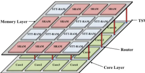
Fig. 1. 3D CMP with hybrid memory system stacked on top of core layer
higher write energy consumption when compared to the traditional SRAM memory technology. In order to overcome the mentioned disadvantages of both memory technologies and benefit from their positive features, we use SRAM and STT-RAM as two different types of memory bank in the memory architecture. This heterogeneous memory design is the best design possibility because it benefits from both memory technologies.
We propose a convex optimization based approach for designing a heterogeneous memory system in order to maximize performance of the three dimensional (3D) CMP with respect to the peak power budget which is the main constraint in the dark silicon era. The proposed model maps applications/threads with more dependency and communication intensity closer to each other while at the same time it finds optimal distance of these applications/threads to each memory banks in order to reduce latency of the 3D CMP design. More specifically, the proposed convex model optimally chooses efficient number and placement of SRAM and STT-RAM memory banks on the memory layer, and maps applications/threads on cores in the core layer.
II. OPTIMIZATION PROBLEM AND FORMULATION
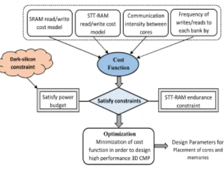
In this section, we propose a convex optimization model with following outputs: 1) optimal placement of SRAM incorporated with STT-RAM banks in the memory layer based on memory access behavior of mapped applications with respect to the peak power budget, 2) Optimal number of SRAM and STT-RAM memory banks, 3) optimal placement of cores by placing threads with more intense communication closer to each other in the core layer. Figure 2 shows block diagram of the proposed convex optimization model.
Core1 Core2 Core3 Core4
Core5 Core6 Core7 Core8
Core9 Core10 Core12
Core16
Core13
Core Layer Router
SRAM SRAM SRAM STT-RAM STT-RAM STT-RAM STT-RAM STT-RAM
SRAM SRAM STT-RAM STT-RAM
SRAM SRAM
STT-RAM SRAM
Memory Layer TSV
Fig. 2. Overview of convex optimization model
The proposed objective function is as follow:
Minimum = ( + ) + . ( + ) (1)
In this Equation, the overall cost is divided to two distinct cost functions related to SRAM and STT-RAM memories as it is shown in Figure 3. is used as a knob for choosing SRAM versus STT-RAM bank in the memory layer. In this model, is a coefficient which can change impact of STT-RAM or SRAM costs in the overall cost function (J). As the target of optimization function is minimizing the overall cost, > 1 results SRAM intensive design, and < 1 results STT-RAM intensive design. Therefore, a designer can tune the model using parameter to design a hybrid memory layer with dominant SRAM or STT-RAM banks.
Fig. 3. Structure of optimization function.
is the communication cost for accessing to SRAM
banks by cores in dimension :
= (( , × , , × ) × ( , , × , , × + , , × , , × )) (2)
In Equation (2), is the number of SRAM banks and its optimal value is found by the proposed model in order to minimize overall cost function. Sum of used STT-RAM and SRAM banks in second layer, and number of cores in first layer are equal to . is dimension of the chip in cordinate. , is communication intensity between cores and . , , is a binary variable and is set to 1 if distance between cores and in -dimension is equal to . In this equation, , , is number of read accesses of core to SRAM bank . Also,
, , is number of write accesses of core to SRAM bank . Note that, these frequencies are available as the proposed optimization model is designed for embedded systems which special purpose applications are run on them. Hence, behavior of these applications are known for us. , , is a binary variable, and it is 1 whether distance between core and
memory bank is equal to . For further illustration Figure 4 shows core layer structure.
Fig. 4. Interconnection between cores in the first layer.
Three left summations in Equation (2) are for finding overall cost of communications between cores in the core layer, and two final summations consider distance and communication between the cores and memory banks. Note that, both of costs are calculated simultaneously and multiplied with each other in order to find . In other words, the cost function can find all possible choices for each application/thread placement in the core layer with each possible placement of SRAM banks in the memory layer while number of SRAM banks can be different in each case. The objective function chooses the best to minimize the overall communication cost based on the design constraints. Similarly, is defined like just for dimension .
is another cost function that is the communication cost for accessing to STT-RAM banks by cores in dimension x. More specifically,
= (( ,× , , × ) ×
( × , , × , , × + × , , × , , × )) (3)
This equation description is like Equation (2) except it models costs of STT-RAM . There are two parameters in Equation (3) that distinct cost function of SRAM and STT-RAM with in this model. In other words, two coefficients namely
and are inserted in the cost function, and they are normalized read and write costs of STT-RAM memory in comparison with SRAM. are defined same as
for dimension .
The total power consumption of the proposed 3D stacked heterogeneous memory architecture during the running phase of the mapped workload must be less than the maximum power budget. In the other word, Equation (4) is the dark silicon constraint for the proposed memory architecture. As we mentioned earlier, a significant amount of on-chip resources cannot be operated at full performance level at the same time due to the dark silicon problem. Our convex optimization model is dark silicon aware since the power budget ( ) is a constraint of this model, and a different hybrid memory layer can be designed based on the power budget value. The total power consumption consists of static and dynamic components and it should be less than the power budget. That is,
= ( + ) ≤ (4) The static power dissipation depends on temperature. Since this optimization approach is solved at design time, we consider
STT-RAM Cost Function X dimension Y dimension SRAM Cost Function X dimension Y dimension Optimization Function 𝝋 Core Layer i i 𝑰 j 𝒊𝒋 j Communication Intensity between two
cores SRAM read/write cost model STT-RAM read/write cost model Communication intensity between cores Frequency of writes/reads to each bank by Cost Function Satisfy power budget STT-RAM endurance constraint Optimization Minimization of cost function in order to design high performance 3D CMP
Design Parameters for
Placement of cores and memories
Dark-silicon
constraint
Satisfy constraints
pessimistic worst-case temperature assumption and calculate and at maximum temperature limit.
= ( , , , × + , , , × ) , = 2 (5)
In Equation (5), , , , indicates whether a SRAM bank is in ( , ) coordinate, and similarly , , , indicates whether a STT-RAM bank is in ( , ) coordinate in layer which is equal to 2 here. This equation finds static power of hybrid memory by adding static power consumption of each SRAM and STT-RAM bank.
In Equation (6), , , and indicate average dynamic power consumed by the SRAM and STT-RAM banks per read and write access, respectively. as
the dynamic power consumption of the proposed hybrid memory system is calculated as bellow:
= ( , , , × , , × + , , ×
+ , , , × , , × + , , × ),
= 2 (6)
We consider endurance problem of STT-RAM banks in our convex optimization model. We propose an endurance model as a constraint in order to decide between two types of memory banks in the hybrid memory architecture. Using this model is due to limited write endurance of STT-RAM which has a direct impact on the life time of the hybrid memory layer. Thus, we can increase lifetime of the design by wisely use of STT-RAM banks. The endurance constraint can be expressed as follows:
∑ , ,
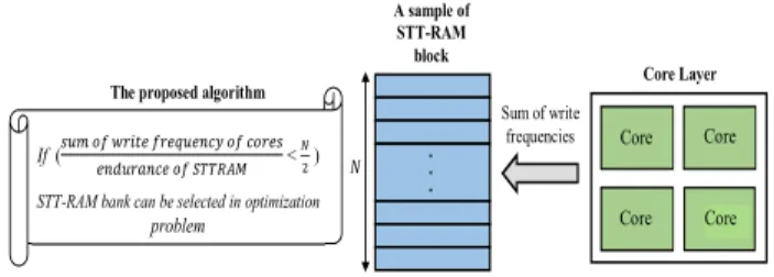
× , , , < 2 , ∀ , , (7) Since STT-RAM has an endurable write threshold, a limited number of writes can be operated in each line of it. If the number of writes into one line is more than the threshold, that line will be destroyed. We assume a worst case scenario that all of write operations are written in one line until destroying that line and after that a new line is selected for rest of write operations. When 50% of lines in a STT-RAM memory bank have been destroyed, a new write operation only has 1/2 chance to go to a valid line which was not destroyed so far. More specifically, there is equal chance of successful or unsuccessful write to the STT-RAM bank. If more than half lines of a STT-RAM banks is destroyed, chance of successful write to this bank is even less than 1/2. Thus, the maximum tolerable destroyed lines for us to use a special STT-RAM bank is N/2. Note that, we assume the number of lines for a STT-RAM bank is equal to N. Thus, in our endurance constraint model, if placing a STT-RAM memory bank in the special position leads to destruction of more than half lines of that memory due to writing frequency of cores, STT-RAM bank is not chosen for that position. Figure 5 shows overview of the proposed endurance model.
Also, sum of used STT-RAM and SRAM banks in second layer is equal to as follow:
( , , , + , , ,) = , = 2 (8)
Note that, our model finds optimal number of SRAM and STT-RAM banks ( , ) and Equation (8) is also a
constraint for finding these variables.
Fig. 5. Model of endurance constraint.
To summarize, objective function J is minimized under constraints (2) through (8). We only mentioned main constraints and their related variables in this section for brevity. Figure 6 shows optimization variables that the hybrid memory layer is designed based on them. These variables (SRC, STC) are optimally found by the proposed model for each eCMP with respect to the running embedded application.
Fig. 6. Design steps of the hybrid memory layer.
III. EXPRIMENTAL EVALUATION
A. Experimental Setup
We use GEM5 [2] as a full system simulator to implement memories and cores. To simulate accurate behaviour of the 3D CMP design and its NoC architecture, we integrated GEM5 with a NoC simulator [3]. In addition, to calculate power consumption of the design, mention platform is integrated with McPAT [4]. The cache capacities and energy consumptions of SRAM and STT-RAM are estimated from CACTI [5] and NVSIM [6], respectively. The simulation platform of the work is shown in Figure 7. Also, the details of the baseline system configuration and parameters that we used in our experiments for SRAM and STT-RAM banks are shown in Table I and Table II, respectively.
We use multithreaded workloads for performing our experiments. The multithreaded applications with small working sets are selected from the PARSEC benchmark suit [7]. In our setup, programs in a given workload are randomly mapped to cores to avoid a specific OS policy. For the
Optimization problem Final hybrid memory architecture SRAM bank placements (SRC) STT-RAM bank placements (STC) 𝑁 Core Layer Sum of write frequencies A sample of STT-RAM block If ( < )
STT-RAM bank can be selected in optimization problem
. . .
The proposed algorithm
Core
Core Core
Core
experimental evaluation, and are considered 100W and 80℃, respectively.
Fig. 7. Simulation platform of the work.
TABLE I. SPECIFICATION OF THE BASELINE EMBEDDED CMP
CONFIGURATION
Component Description Number of Cores 16, 4× 4 mesh
Core Configuration
Alpha21164, 3GHz, area 3.5mm2, 32nm
Private Cache per
each Core SRAM, 4 way, 32B line, size 32KB per core On-chip Memory
Hybrid-fix: 8MB SRAM (8 banks , each 1MB) and 32MB STTRAM (8 banks , each 4MB )
Network Router
2-stage wormhole switched, virtual channel flow control, 2 VCs per port, a buffer with depth of 4 flits per each VC, 5 flits buffer depth, 8 flits per Data Packet, 1 flit per address packet, each flit is set to be 16-byte long
TABLE II. DIFFERENT MEMORY TECHNOLOGIES COMPARISON AT 32NM
Technology Area Latency Read Write Latency
Leakage Power at ℃
Read
Energy Energy Write
1MB
SRAM 3.03 0.702ns 0.702ns 444.6mW 0.168nJ 0.168nJ
4MB
STT-RAM 3.39 0.880ns 10.67ns 190.5mW 0.278nJ 0.765nJ
B. Experimental Result
In this section, we evaluate our proposed 3D CMP with stacked memory in two different cases: 1) the CMP with hybrid stacked memory with same number of SRAM and STT-RAM banks in which STT-RAM banks are on the left and SRAM banks are on the right part of the memory layer (Hybrid-fix), 2) CMP with the proposed hybrid stacked memory on the core layer.
Figure 8 shows the results of normalized energy consumption. As shown in this figure, the proposed design reduces energy consumption by about 31.3% on average compared to Hybrid-fix design.
Figure 9 compares the normalized performance results. As shown in this figure, the proposed design improves performance up to 14.7% (7.54% on average) compared to the Hybrid-fix baseline design.
Figure 10 compares life time of the proposed design with Hybrid-fix design for each benchmark.The proposed hybrid memory architecture shows 4.27 times (on average) up to 8.3 times improvement in life time compared with Hybrid-fix
memory design.
Fig. 8. Normalizedenergy consumption of the proposed design with respect to Hybrid-fix.
Fig. 9. Normalized performance comparison of each application with respect
Fig. 10. Life time comparison of the proposed memory with Hybrid-fix design.
IV. CONCLUSION
In this work, we proposed a model to design an optimal heterogeneous memory system with using SRAM and STT-RAM memory banks. Our proposed convex optimization-based model finds optimal number and placement of different memory banks to satisfy peak power budget which is the main challenge in the dark silicon era. Experimental results show that the proposed method improves energy consumption by 31.3% on average compared to the baseline hybrid design.
REFERENCES
[1] H. Esmaeilzadeh, E. Blem, R. S. Amant, K. Sankaralingam, and D. Burger. "Dark silicon and the end of multicore scaling," In Computer Architecture (ISCA), pp. 365-376, 2011
[2] N. Binkert, et al. “The gem5 simulator.” ACM SIGARCH Computer Architecture News 39, vol. 39, no. 2, May 2011.
[3] M. Palesi, S. Kumar and D. Patti, “Noxim: Network-on-chip simulator,” http://noxim.sourceforge.net, 2010.
[4] S. Li, et al, “McPAT: an integrated power, area, and timing modeling framework for multicore and manycore architectures,” In Annual IEEE/ACM International Symposium on MICRO-42, pp. 469-480, 2009. [5] N. Muralimanohar, R. Balasubramonian and N. P. Jouppi, “CACTI 6.0: A tool to model large caches,” HP Laboratories, Technical Report, 2009. [6] X. Dong, C. Xu, N. Jouppi, and Y. Xie, “NVSim: A Circuit-Level Performance, Energy, and Area Model for Emerging Non-volatile Memory,” In Emerging Memory Technologies Springer, pp. 15-50, New York, 2012.
[7] M. Gebhart, et al. "Running PARSEC 2.1 on M5." University of Texas at Austin, Department of Computer Science, Technical Report, 2009.
Gem5 3D Noxim ORION 3 Power Unit NVsim CACTI McPAT Blackschole, Bodytrack, Caneal, Fuidanimate, Swaptions, Ferret, Vips
PARSEC workloads 0.2 0.4 0.6 0.8 1 1.2 E n e rg y co ns u m pt io n (N o rma li ze d) Proposed Hybrid-fix 0 0.2 0.4 0.6 0.8 1 1.2 Lif et ime (Normaliz e d ) Proposed Hybrid-fix 0.9 0.95 1 1.05 1.1 1.15 1.2 IPC (N ormal iz ed) Proposed Hybrid-fix 2610