CONTROLLING
ELECTROMAGNETIC WAVES
WITH ACTIVE GRAPHENE DEVICES
A THESIS SUBMITTED TO
THE GRADUATE SCHOOL OF ENGINEERING AND SCIENCE OF BILKENT UNIVERSITY
IN PARTIAL FULFILLMENT OF THE REQUIREMENTS FOR
THE DEGREE OF DOCTOR OF PHILOSOPHY IN PHYSICS
By
Osman Balcı
September, 2015
i
CONTROLLING ELECTROMAGNETIC WAVES WITH ACTIVE GRAPHENE DEVICES
By Osman Balcı September, 2015
We certify that we have read this thesis and that in our opinion it is fully adequate, in scope and in quality, as a dissertation for the degree of Doctor of Philosophy.
___________________________________________ Asst. Prof. Dr. Coşkun Kocabaş (Advisor)
___________________________________________ Prof. Dr. Hayrettin Köymen
___________________________________________ Prof. Dr. Oğuz Gülseren
___________________________________________ Prof. Dr. Raşit Turan
___________________________________________ Assoc. Prof. Dr. Hakan Altan
Approved for the Graduate School of Engineering and Science:
___________________________________________ Prof. Dr. Levent Onural
ii
Copyright Information
Copyright © 2015 Nature Publishing Group. Some figures and sections in chapter 2, 3, and 4 is reprinted with permission from O. Balci, E.O. Polat, N. Kakenov, C. Kocabas, “Graphene-enabled electrically switchable radar absorbing surfaces”
iii
ABSTRACT
CONTROLLING ELECTROMAGNETIC WAVES
WITH ACTIVE GRAPHENE DEVICES
Osman Balcı Ph.D. in Physics
Advisor: Asst. Prof. Dr. Coşkun Kocabaş September, 2015
The dynamic control of electromagnetic waves forms the basis of modern communication technologies. Although sources of microwaves can be controlled by electrical means, the active control of microwaves in the free space has been a challenge due to the lack of an active material. Graphene, the 2-dimensional crystal of carbon, provides a unique platform to control light-matter interaction in a broad spectrum. This thesis describes a new approach to control microwaves using large area active graphene devices. Our strategy relies on electrostatic tuning of the density of high mobility charge carriers on an atomically thin graphene electrode which operates as a tunable metal in microwave frequencies. We developed a method to synthesize large area graphene (20x20 cm2) by chemical vapor deposition. Using large area graphene electrodes, we demonstrate a new class of active surfaces capable of real-time electrical control of reflection, transmission, and absorption of microwaves over a broad spectrum. These active devices allow us to fabricate electrically tunable microwave surfaces such as switchable radar absorbing surfaces and tunable metamaterials with modulation depth of 50𝑑𝐵 and operation voltage of 3𝑉. Large modulation depth, simple device architecture, and mechanical flexibility are the key attributes of the graphene-enabled active microwave surfaces that could find a wide range of applications ranging from active signal processing to adaptive camouflage.
iv
ÖZET
ELEKTROMANYETİK DALGALARIN AKTİF
GRAFEN AYGITLARI İLE KONTROL EDİLMESİ
Osman Balcı Fizik, Doktora
Tez Danışmanı: Yr. Doç. Dr. Coşkun Kocabaş Eylül, 2015
Elektromanyetik dalgaların dinamik olarak kontrol edilmesi modern iletişim teknolojilerinin temelini oluşturmaktadır. Mikrodalga kaynaklarının kolaylıkla kontrol edilebiliyor olmasına rağmen, kaynaktan ayrılan mikrodalgaların boş uzayda kontrol edilmesi mikrodalgada kullanılabilecek aktif bir malzemenin olmayışından dolayı çözülmesi gereken çok önemli bir problemdir. Bu tezde geniş alanlı grafenden elde edilmiş aygıtlar kullanarak mikrodalgaların yeni bir yaklaşım ile kontrol edilmesi anlatılmaktadır. Kullandığımız teknikte atomik derecede ince olan ve mikrodalga frekanlarında degişken bir metal gibi davranabilen grafen elektrotlar üzerindeki yük yoğunluğunu elektrostatik olarak kontrol ediyoruz. Geniş alanlı (20x20cm2) grafen tabakaları kimyasal buhar yükleme sistemi kullanılarak sentezlenmiştir. Bu geniş alanlı grafen tabakalarını kullanarak geliştirdiğimiz aygıt sayesinde mikrodalgaların geniş bir band aralığında geçirgenliğini, yansımasını, ve emilmesini elektriksel olarak kontrol edebiliyoruz. Bu aktif yüzeyler sayesinde açılıp kapatılabilir radar emici yüzeyler ve kontrol edilebilir metamalzemeler 50dB genlik seviyelerine kadar sadece 3V voltaj uygulayarak kontrol edilebilmiştir. Yüksek mudülasyon oranı, basit aygıt yapısı ve meknik esnekliği, üretilen mikrodalga modülatörlerinin en önemli özellikleri ve bu aygıtlar aktif sinyal işletiminde, kontrollü görünmezlik araştırmalarında geniş bir uygulama alanı bulabilir.
Anahtar sözcükler: Grafen, mikrodalga modülatörler, radar emiciler, aktif
v
Acknowledgement
Although this thesis belongs to me, many people contributed to this thesis. This short acknowledgement section is not enough to thank all of them one by one hence I would like to thank everyone contributing to this theses all at once here.
I have been educated in Bilkent University with a full scholarship during both my B.S. and Ph.D. study. I learned almost everything that I know in Bilkent University. Therefore, I would like to first thank to Bilkent University for giving me such a unique and high quality scientific and social education.
It was an honor and great chance for me to work with my advisor Asst. Prof. Dr. Coskun Kocabas during my Ph.D. study. He has endless ambition to work without considering the time. We have found a lot of new ideas and methods together during “Friday afternoon” experiments. His quick and smart problem solving ability save me from many desperate conditions. He taught me many useful “research hacks” that I will certainly use in my future life. We spent almost six years in my Ph.D. study, I owe all my scientific achievements to him. I learned a lot from him, I will follow his lead in the future. I would like to express my sincere thanks and gratitude to him for everything.
I am grateful to members of my thesis committee Prof. Dr. Oğuz Gülseren and Prof. Dr. Hayrettin Köymen. They attended eight thesis progress presentations and they supported and guided me through all my PhD. study.
I would like to thank diroctory of Advanced Research Labarator (ARL), Prof. Dr. Atilla Aydınlı. He spent a lot of time for the problems of ARL and he provided us one of the best labaratory and office conditions in Turkey.
I would like to express my gratitute to my brother Asst. Prof. Dr. Sinan Balci and also his family. He encouraged me to work in the hard times of my Ph.D. He shared
vi
his valuable scientific experiences with me throughout my Ph.D. He and his family made me to feel not alone through six years. We had many discussions together on scientific, family, social and daily topics. Thank you brother for everything.
I would like to express my gratitude to all current and former group mates; Dr. Omer Salihoglu, Dr. Emre Ozan Polat, Nurbek Kakenov, Dr. Ivgenia Kovalska, Shahnaz Aas, Pınar Köç, Erçağ Pinçe, Melih Okan. We worked on different projects together, I learned many things from each of them. They helped me a lot during my Ph.D. study and they had a considerable amount of contribution to this thesis. They are all friendly and hardworking scientists, I am sure each of them will be in the position that they want to be. I will miss our discussions in the office. Many thanks to each of them.
I would like to thank undergrads Onur Çakıroğlu, Burkay Uzlu, and Muhammed Bilgin. We work together in the last months of my Ph.D., they are such a hardworking and smart guys.
I would like to thank Prof. Dr. Ekmel Özbay, Dr. Semih Çakmakyapan and Dr. Ertuğrul Karademir for colobrating with us for the simulation of active metadevices. I would like to thank Ergün Karaman, Elvan Ogün and all the ARL stuffs for their valuable technical and secreterial support.
I would like to thank TÜBİTAK-BİDEB for the scholarship program 2211- DOKTORA BURS PROGRAMI in which I had been a scholar.
I would like to thank TÜBİTAK for the projects (114F052, 113F278, 112T686, 109T259) which I worked in and got scholarship from.
I would like to thank all my family; my mother Şadiye Balcı, my father Mustafa Balcı, my brothers, and my sisters. I could not succeed anything without you. Finally, I would like to thank my wife Hatice Balcı and my son Mustafa Selim Balcı. Everything I achieved is yours. I dedicate this thesis to you.
vii
viii
Contents
1 Introduction ... 1
1.1. Electronic band structure of graphene ... 7
1.2. Optical Conductivity of graphene ... 13
2 Interaction of light with Graphene ... 23
2.1. Transfer matrix method ... 24
2.1.1. Simulation of single layer graphene ... 24
2.1.2. Simulation of two layer graphene stack ... 35
2.1.3. Simulation of multiple graphene layers stack ... 39
2.2. Transmission line model ... 42
2.3. Simulation of graphene supercapacitor ... 44
3 Fabrication of large area graphene supercapacitors ... 50
3.1. Synthesis of graphene ... 51
3.1.1. Transfer of graphene ... 53
3.1.2. Electrical and optical characterization of single layer graphene ... 58
3.2. Large area graphene supercapacitors ... 65
3.2.1. Electrical characterization of graphene supercapacitors ... 66
3.2.2. Optical spectroscopy of graphene supercapacitors ... 72
4 Graphene-enabled electrically switchable radar absorbing surfaces ... 77
4.1. Adaptive Microwave Surfaces ... 79
ix
4.3. Discussion ... 100
5 Electrically switchable metadevices ... 104
5.1. Electromagnetic modelling ... 106
5.2. Fabrication of graphene metadevice ... 109
5.3. Microwave response of graphene metadevice ... 114
x
List of Figures
Figure 1.1 Graphene based optoelectronic devices working in various wavelengths investigated by our group. The highlighted devices in the microwave regime are investigated during my Ph.D. study. This thesis will describe the fabrication and characterization of these devices. The graph shows the calculated optical absorption of single layer graphene which yields controllable optical absorption in a very broad electromagnetic spectrum. Although the amount of absorption in visible and infrared wavelengths is small, especially for the long wavelength region tunability is as high as 50%. ... 2
Figure 1.2 Comparison of (a) a dielectric capacitor and (b) a graphene supercapacitor. ... 4
Figure 1.3 The photograph of large area graphene supercapacitor (a) and schematic explanation of ionic gating of graphene electrodes by an ionic liquid (b). ... 6
Figure 1.4: Schematic drawing of hexagonal lattice structure of graphene. Red and blue dots represent the carbon atoms in graphene structure and red dots are assumed to be the lattice points for a triangular lattice. Blue dots are sub-lattices which are connected to a lattice point with a basis vector. Here we assume any one of 𝑏1,2,3 vectors as a basis vector. The vectors 𝑎1 and 𝑎2 are lattice vectors and 𝑏1, 𝑏2 and 𝑏3 are the vectors showing the nearest neighbor position of a carbon atom relative to a lattice point. The side length of a hexagon is 𝑎. ... 9 Figure 1.5 Electronic band structure of graphene calculated using the tight binding method. The figure on the left shows the energies of the bands in the first Brillouin zone of graphene. Conduction and valance bands are not symmetric at higher energies but they are symmetric at lower energies near Dirac point as shown in the right plot.
xi
Here we used 𝜀2𝑝 = 0, 𝑡 = −3.033𝑒𝑉, and 𝑠 = 0.129 for the parameters in Eq.(1.12). ... 12
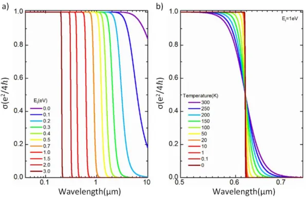
Figure 1.6 Optical conductivity of graphene due to interband transitions with varying Fermi energies (a) and with varying temperatures (b). Graphene has a constant optical conductivity in a broad spectrum when the Fermi energy coincides with Dirac point. If the Fermi energy is shifted up or down to the Dirac point by chemical or electrical doping, optical conductivity of graphene goes down to zero for energies lower than two times the Fermi energy due to Pauli blocking of transitions from valance band to conduction band. Optical conductivity of graphene depends on the temperature. Electrons obey Fermi-Dirac statistics, therefore the behavior of Pauli blocking is sharp at low temperatures. Due to thermal fluctuations, the step function due to Pauli blocking becomes broader as temperature increases. ... 15
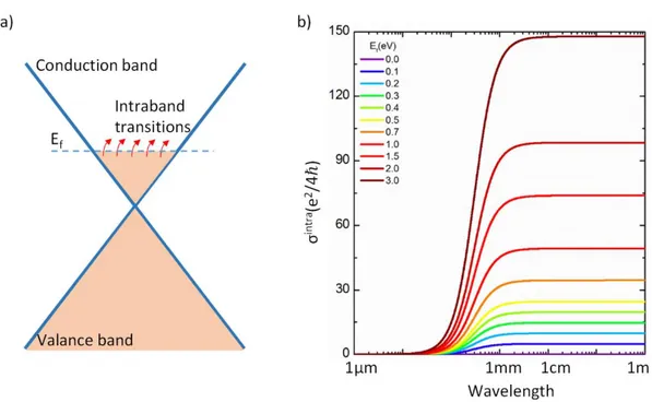
Figure 1.7 Intraband conductivity of graphene for various Fermi level energies of graphene in the unit of universal conductivity of graphene. When Fermi level of graphene is at Dirac point, there is no electron in the conduction and no holes in the valance bands, and therefore, intraband conductivity of graphene is zero. If the Fermi level of graphene is in the conduction or valance band, then there are filled energy levels in graphene and intraband conductivity of graphene is nonzero. Intraband conductivity of graphene increases with an increase in the Fermi energy of graphene. ... 19
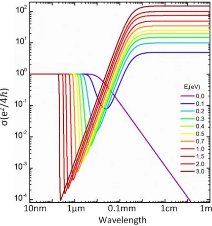
Figure 1.8 Total conductivity of graphene in the unit of universal conductivity 𝑒2/4ℏ for varying Fermi energies in a broad wavelength spectrum ranging from 10nm to 1m. Conductivity of graphene is dominated by the interband conductivity in short wavelengths. Interband contribution can be suppressed even for short wavelengths by increasing the Fermi level of graphene. For longer wavelengths, conductivity of graphene is dominated by the intraband conductivity of graphene. In this case, the
xii
intraband conductivity increases with an increase in the Fermi level energy of graphene opposite to the interband case. ... 22
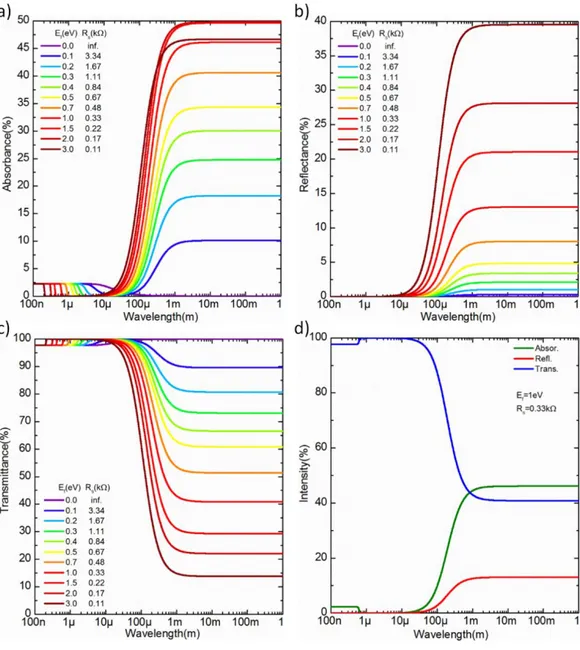
Figure 2.1 Schematic drawing of the geometry used for the calculation of optical response of a single layer graphene. A graphene layer with a conductivity of 𝜎 is surrounded by two different mediums having dielectric constants of 𝜀1 and 𝜀2. All of the incoming and outgoing electromagnetic waves are considered to have amplitudes of 𝑎1, 𝑎2, 𝑏1, 𝑏2 and angle of incidence of 𝜃1, 𝜃2. ... 25 Figure 2.2 Calculated optical response of a single layer graphene in a broad wavelength range is demonstrated. Absorbance (a) of graphene depends on the incident wavelength. The maximum absorbance of a single layer graphene is ~%2.24 in the visible, and %50 in the microwave. Absorbance of graphene varies with the Fermi energy of graphene. Reflectance (b) and transmittance (c) of graphene are due to the interband and intraband conductivity of graphene and it can be tuned by tuning the Fermi level of graphene. Absorbance, reflectance, and transmittance of graphene with a Fermi energy of 1𝑒𝑉 is shown in (d). ... 29 Figure 2.3 Absorbance (green), reflectance (red), and transmittance (blue) of a single layer graphene as a function of sheet resistance (𝑅𝑠) are shown. The wavelength of the incident electromagnetic radiations is 3𝑐𝑚(a), 0.3𝑚𝑚(b), 10𝜇𝑚(c), and 800𝑛𝑚(d). In the microwave region, the maximum absorbance (%50) can be achieved when the impedance of single layer graphene is matched to half of the free space impedance, i.e. 186.5𝛺 (a). For the terahertz (b) and infrared (c) regions of electromagnetic spectrum, both the maximum absorbance and the required impedance are decreasing. In the visible spectrum, graphene absorbs ~2.24% for electromagnetic energies above two times the Fermi energy of graphene. ... 32
Figure 2.4 Calculated optical response of single layer graphene for various angle of incidences with the wavelength of 3𝑐𝑚. (a) Absorbance as a function of sheet resistance of graphene is shown for s-polarized incident radiation. Colored lines
xiii
specify the different angle of incidences. (b) Absorbance, reflectance and transmittance of one layer graphene as a function of incident angle for s-polarized radiation at the sheet resistance of 1𝑘𝛺 are designated. (c) Absorbance of p-polarized radiation with a wavelength of 3𝑐𝑚 as a function of sheet resistance of graphene for various incidence angles is shown. (d) Absorbance, reflectance and transmittance of graphene at 1𝑘𝛺 sheet resistance as a function of angle is displayed. ... 34 Figure 2.5 Schematic drawing of a single layer graphene in two different layers is shown. There are three different dielectric mediums possessing dielectric constants of 𝜀1, 𝜀2, 𝜀3. Two different graphene layers are between these three mediums. Second medium is between two layers of graphene and has a thickness of 𝐿2. ... 37
Figure 2.6 Simulated optical response of two stacks of graphene layers. The distance between two graphene layers is assumed to be 50𝜇𝑚 and they are assumed to be in the free space. Due to the separation between two graphene layers, there are Fabry-Perot resonance peaks in the absorbance spectrum and absorbance goes over %70 in the THz frequencies (a, b). Varying the sheet resistance of graphene layers tunes the absorbance, reflectance, and transmittance of two graphene layers for the wavelength of 3𝑐𝑚 (c) and 0.3𝑚𝑚 (d). The calculated maximum absorbance value in this condition is still %50 in the microwave region. ... 38 Figure 2.7 Simulated optical response of 10 stacks of graphene layers is shown. All graphene layers are assumed to be identical and they are separated with a distance of 50𝜇𝑚. They are all assumed to be in the free space. Absorbance spectrum of 10 graphene stacks is shown in (a) for varying Fermi energies. Absorbance, transmittance, and reflectance spectra are shown in (b) for 1𝑒𝑉 Fermi energy from 10𝑛𝑚 to 1𝑚. Varying the sheet resistance of graphene layers tunes the optical response of the 10 stacks of graphene layers in the microwave frequencies with the wavelength of 3𝑐𝑚 as shown in (c) and for terahertz frequencies with the wavelength of 0.3𝑚𝑚 as shown in (d) ... 41
xiv
Figure 2.8 Optical response of a single layer graphene calculated with transmission line model for normal incidence. Absorbance (a), reflectance (b) and transmittance (c) as a function of incident wavelength for various Fermi energies are plotted. Absorbance (green), reflectance (red), and transmittance (blue) as a function of sheet resistance of single layer graphene for the incident wavelength of 3𝑐𝑚 are shown in (d). ... 43
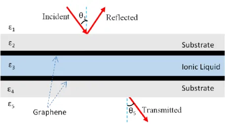
Figure 2.9 Schematic representation of a drawn graphene supercapacitor which used in the transfer matrix calculations. ... 44
Figure 2.10 Simulated optical response of graphene supercapacitor including the dielectric constants of supporting substrates and ionic liquid. (a) Absorbance, reflectance, and transmittance of incident radiation with 3𝑐𝑚 wavelength. It is assumed that the angle of incidence is 30𝑜. Absorbance (b), reflectance (c), and transmittance (d) as function of wavelength ranging from 100𝑛𝑚 to 1𝑚 for various Fermi energies and sheet resistances of one layer graphene in a graphene supercapacitor. At short wavelengths, there are interference effects especially in the far-infrared and terahertz frequencies due to the comparable length scales between thicknesses of layers and wavelengths. ... 45
Figure 2.11 Optical response of a graphene supercapacitor for various angle of incidences for an s-polarized radiation. Absorbance (a), reflectance (b), and transmittance (c) of the device as function of sheet resistance are graphed. As the angle of incidence increases, incident radiation experiences more impedance. Absorbance reaches its maximum value at high sheet resistance of single layer graphene. (a) Absorbance, reflectance, and transmittance of the device at 1𝑘𝛺 sheet resistance are shown. ... 47
Figure 2.12 Optical response of graphene capacitor is shown for p-polarized radiation. Absorbance (a), reflectance (b), and transmittance (c) are plotted as a function of sheet resistance of graphene layers. For p-polarization, peak position of
xv
the absorbance shifts to smaller resistances as the angle of incidence increases. Absorbance and reflectance decrease and transmittance increases as the angle of incidence increases, (d). ... 48
Figure 3.1 Photographs of the smooth copper and the high temperature furnace. Before starting growth process, the smooth copper foils are cut according to the size of the flat quartz holder and then the copper foils are located on the holder as shown in a). Quartz holder has 30𝑐𝑚 length and 7𝑐𝑚 width, the diameter of the quartz chamber is 8𝑐𝑚. The holder is located at the center of the quartz chamber and the chamber is vacuumed with an oil pump. Then the foils are heated until 1035𝑜𝐶 under 100𝑠𝑐𝑐𝑚 𝐻2flow by using a double zone high temperature split furnace with a width of 60𝑐𝑚 shown in b). Graphene is grown by sending 10𝑠𝑐𝑐𝑚 of 𝐶𝐻4 with 100𝑠𝑐𝑐𝑚 𝐻2 for 10𝑠. After growth of graphene, copper foils are removed from the furnace after cooling furnace down to the room temperature under 100𝑠𝑐𝑐𝑚 𝐻2 as shown in c). ... 53
Figure 3.2 Schematic demonstration of the graphene welding process of two pieces of graphene grown copper foils. After synthesis of graphene on copper foils, copper foils are located on the fusible side of a PVC substrate with a short overlap as the graphene grown sides are on the PVC substrate. Subsequently, an A4 paper sheet was laid on the overlapping copper foils as a back support and the whole sample is laminated by using a hot lamination machine. Before laminating process, there is a gap between two copper foils and PVC substrate at the intersection area. When two copper foils are laminated, the gap between the two copper foils is filled with melted PVC and thus two graphene layers are welded to each other at the intersection point. After etching copper foils, welded and electrically contacted graphene layers on PVC remain on the surface of PVC. ... 55
Figure 3.3 Transfer process of graphene on copper foils to the PVC substrate by using a hot laminating machine is shown. Graphene grown on copper foils are located
xvi
between a paper and a PVC film as in a). Then two graphene layers are welded as explained in Figure 3.2 and shown in b). Graphene grown on the top surface of the copper foils is transferred and therefore the fusible side of the PVC film is put on top of the copper foils as shown in a) and b). Finally, paper-copper-PVC stack is laminated in a hot laminating machine as shown in c), d) and e). The temperature of the laminating machine is ~120𝑜𝐶. Laminated and welded graphene grown copper foils are shown in f). ... 56
Figure 3.4 Chemical etching process of laminated graphene layers grown on copper is shown. Two tapes are used to cover the two ends of laminated copper foils in order not to etch copper foils under the tape, a). Electrical contact from the transferred graphene layers are taken by using copper foils that are used for graphene growth. The copper foils are chemically etched in ~5𝑚𝑀 aqueous solution of 𝐹𝐶𝑙3 in ~10𝑚𝑖𝑛. as shown in b) and c). After washing in a clean DI water and drying, graphene layers on the PVC having two copper contacts is obtained as in d). ... 57
Figure 3.5 Transmission measurement of large area graphene transferred on PVC substrate. The photograph of a single layer graphene on a PVC substrate having two copper contact lines is shown in (a). FTIR spectrometer is used for the transmission measurements, where the transmission of graphene transferred on PVC substrate has been taken and normalized to a reference signal from a PVC substrate without graphene, (b). Due to the excitonic contribution to the absorbance of graphene, transmission decreases for higher energies as shown in (b). ... 60
Figure 3.6 Optical Raman spectroscopy spectrum of single layer graphene transferred to a glass substrate. The photograph of the graphene on glass is shown in (a). Thanks to the absorption of single layer graphene absorbing ~%2.24 in the visible spectrum, graphene is darker than glass in the photograph. Typical Raman peaks of single layer graphene are shown, a laser with a wavelength of 632𝑛𝑚 is used. 2D band is at
xvii
2700𝑐𝑚 − 1 and G band is at 1600𝑐𝑚 − 1 wavenumber. The intensity ratio of G band to the 2D band is 1.36. ... 61 Figure 3.7 Electrical characterization of single layer graphene on PVC substrate is shown. Total resistances of the graphene on PVC substrates with different lengths are measured as in (a). Then the measured resistance is multiplied with the width of the graphene on PVC substrate and plotted as a function of graphene length as shown in (b). The slope of the fitted line gives the sheet resistance of graphene, which is 𝑅𝑠 = 3.32𝑘𝛺/𝑠𝑞. The resistance value at which the fitted line intersects at zero length is two times the contact resistance of graphene to copper foil contacts having the width of 1𝑐𝑚. Here the contact resistance is calculated as ~𝑅𝑐 = 0.7𝑘𝛺. 𝑐𝑚. The circuit diagram of a graphene layer on PVC substrate with two copper contacts is drawn in (c). There are two contact resistances due to two copper foil contacts and also one sheet resistance which is the sheet resistance of graphene sheet. ... 64
Figure 3.8 Large area graphene supercapacitor is shown. a) Schematic representation of graphene supercapacitor; there are two graphene electrodes and there is an ionic liquid between these two graphene electrodes. A bias voltage is applied between these two graphene electrodes and the ionic liquid is polarized. Negative ions are collected at positive bias applied graphene electrode and positive ions are collected at negative bias applied graphene electrode. Collected ions create ~1𝑛𝑚 thick electrical double layer (EDL) at graphene-ionic liquid interface. Photograph of the fabricated graphene supercapacitor is shown in b). ... 66
Figure 3.9 Electrical characterization of fabricated large area graphene supercapacitors. (a) Circuit diagram of graphene supercapacitor is shown, graphene electrodes are represented with a tunable capacitance 𝐶𝑞 and resistance 𝑅𝑠 and electrolyte is represented with a resistance 𝑅𝑒 and a capacitance 𝐶𝑒. (b) Modulation of 𝐶𝑞 and 𝑅𝑠 as a function of voltage is shown. (c) Cyclic voltammetry of graphene supercapacitor is shown, charging and discharging of the capacitor at various scan
xviii
rates is plotted. (d) We measured time response for charging and discharging of graphene supercapacitor. We apply 3𝑉 for charging and 0𝑉 for discharging and record current for the time trace. Time response of both charging and discharging is ~1𝑠. ... 68 Figure 3.10 Leakage current and hysteresis observed in the transport measurements. (a) Nonlinear RC circuit model used to characterize the leakage current of the graphene super capacitor. (b) Leakage current of the graphene capacitor as a function of bias voltage between the graphene electrodes. (c) Variation of the resistance of graphene electrodes with bias voltage. (d) Variation of the total capacitance of the graphene supercapacitor. In the transport measurements we observed a slight hysteresis. ... 70
Figure 3.11 Simulated charging and discharging behavior of graphene supercapacitor obtained from the circuit simulator (Advanced Design System (ADS), Agilent). The total charge on the graphene capacitor derived by a square pulse with 30s period and 50% duty cycle. ... 71
Figure 3.12 Optical characterization of graphene supercapacitors. (a) Schematic drawing of the graphene capacitor and FTIR beam are shown. (b) Modulation of the optical transmission at various bias voltages. Modulation shows a step like spectra with a cutoff at 2Ef. Two overlapped step-like modulation associated with the bottom
and top graphene electrodes are observed. (c) The extracted Fermi energies of the top and bottom graphene electrodes from the optical transmission modulation spectra. (d) The calculated charge densities on the top and bottom graphene electrodes from the extracted Fermi energies. ... 73
Figure 3.13 Electrical parameters extracted from the transport and optical measurements. (a) Correlation of the Fermi energy with the sheet resistance of the graphene electrode. (b) Charge density vs. Sheet resistance, (c), Extracted charge mobility vs. sheet resistance and (d), Extracted mobility vs. charge density. ... 75
xix
Figure 4.1(a) Schematic representation of the graphene-based adaptive microwave surfaces. The device consists of two large-area graphene electrodes transfer printed on a microwave-transparent PVC support and electrolyte between them. (b) Cross-sectional view of the device. Application of a voltage bias polarizes the electrolyte (ionic liquid) and forms ionic double layers on the graphene–electrolyte interface.81
Figure 4.2 (a) Photograph of the fabricated device. (b) Representation of the electronic band structure of graphene and electronic transitions that defines the broadband optical response. ... 82
Figure 4.3 Calculated broadband absorption of a single layer graphene with different sheet resistance for the electromagnetic spectrum covering from the visible to microwave frequencies. ... 83
Figure 4.4 Microwave characterization of the adaptive microwave surfaces. (a) Experimental setup used for the microwave measurements. A microwave transmitter with a power of 15mW at 10.5 GHz and two receivers were used to measure the reflected and transmitted microwave power. (b, c) Measured intensity of the reflected and transmitted microwaves plotted against the bias voltage. (d) The extracted microwave absorption of the graphene capacitor as a function of bias voltage. ... 85
Figure 4.5 (a) Measured resistance of graphene electrodes (including contact resistance) as a function of bias voltage. (b) The experimental (scattered plot) and calculated (solid lines) microwave reflection, transmission and absorption are plotted against sheet resistance. (c, d) Real-time microwave reflection, and transmission, through the graphene capacitor during periodic charging and discharging. The RC response time of the capacitor is determined by the varying resistance of the graphene electrodes and the total capacitance of the device. The extracted response time of graphene capacitor with dimensions of 8x8cm2 is around 300ms. ... 87
xx
Figure 4.6 Graphene based switchable radar absorbing surfaces. (a) Schematic representation of the resonant device including the graphene capacitor and metallic surface placed at a distance of quarter-wavelength. (b, c) Photographs of the front and the back side of the fabricated device. ... 90
Figure 4.7 (a) Measured microwave reflection at 10.5 GHz plotted against the bias voltage. The red curve shows the reflection in decibel. (b) Real time reflection from the device during periodic charging and discharging. The device yields around 50 dB reflection suppression ration. ... 92
Figure 4.8 (a) Broad–band reflection spectrum from the device at various bias voltages. The noise floor is at -80dB. (b) Microwave reflection from the device plotted against the bias voltage and the spacer thickness which defines the distance between the graphene electrodes and metallic surface. ... 92
Figure 4.9 (a) Variation of the modulation depth of the resonant device with the spacer thickness. When the graphene is at the antinodes, the modulation is around 100% whereas, at the nodes the modulation is close to zero. (b) Broadband reflection spectra from the device for three different spacer thickness. ... 93
Figure 4.10 (a) Reflection vs. voltage for two different distances. (c, d) Transmission line model for the resonant surface. Graphene electrodes are represented by variable resistance and the metallic surface is represented by a line which shorts the ports. 93
Figure 4.11 (a) Variation of the microwave reflection from the surface of the resonant device with different incidence angle (inset shows the incidence angle). (b) The modulation depth and (c) on-off ratio plotted against incidence angle. ... 94
Figure 4.12 (a) Photograph of the pixelated microwave surface consist of 14 individually addressable hexagonal shaped cells. (b, c) Photograph of the front and back side of an individual cell. ... 94
xxi
Figure 4.13 (a) Exploited view of the structure of an individual cell showing the layers. (b) Microwave reflection of an individual cell at 10.5 GHz. ... 96
Figure 4.14 Scanning microwave reflection images of an hexagonal cell at different bias voltages. ... 97
Figure 4.15 Scanning microwave reflection of 4 cells with different voltage configurations. ... 98
Figure 4.16 Non-planar adaptive radar absorbing surfaces. (a, b) Photograph of concave and convex hemispherical surfaces formed by individually addressable hexagon and pentagon shaped adaptive cells. (c) Photograph of the cylindrical-shaped switchable radar absorbing surface placed around a metallic cylinder. The diameter of the cylinder is 4.2 cm. ... 99
Figure 4.17 (a) Reflection from the cylindrical surface containing a metallic cylinder as a function of bias voltage. (b) Orientation dependence of the normalized reflection from the surface at 0 and 2V, respectively. At 2V the reflectivity is suppressed by 50dB for all directions. The variation of the intensity on the off-state is due the variation of the distance between the graphene electrodes and metallic cylinder. 100
Figure 5.1 Tunable graphene-SRR hybrid metamaterial: a) Schematic representation of the hybrid metamaterial consisting of split ring resonator capacitively coupled to the graphene layer. The capacitive coupling is defined by the SRR-graphene separation, d. b) Small signal equivalent model of the graphene-SRR hybrid metamaterial. SRR is represented by the L, R, C lump circuit elements; the graphene layer is modeled by the variable sheet resistance, RG and quantum capacitance, CQ.
Cc models the capacitive coupling. ... 107
Figure 5.2 Simulated S21 values for a graphene-SRR hybrid metamaterial: a)
xxii
sheet resistance of graphene. b) Calculated transmittance spectra for various sheet resistance of graphene (10 to 0.5 kΩ) at graphene-SRR distance of 0.5 mm. ... 109 Figure 5.3 Fabrication of large area split ring resonator structure. a) A PVC film is laminated on 10μm thick, clean copper foil. SRR structure is printed on the laminated copper foil by using HP color laser jet printer (CP2020). The printed toner works as an etch mask. b), c) After printing SRR structure on laminated copper foil, the copper foil is etched in a nitric acid aqueous solution. The printed SRR patterns masks the laminated copper film to form SRR structure hence un-printed area on the copper is etched. d) Picture of the fabricated SRR structure on PVC substrate after washing and drying is shown. ... 111
Figure 5.4 Lamination of fabricated SRR arrays on a graphene transferred PVC. a) Single layer graphene is grown on large area copper film and laminated onto polymer film (PVC). b) The SRR is laminated on graphene-grown copper. The four layers of PVC films are inserted between graphene grown copper and the SRR structure as a spacer between graphene and SRR array. c) Laminated SRR array on top of graphene grown copper. d) SRR laminated graphene grown copper is shown. The layers from top to bottom: SRR arrays, multiple PVC films, graphene grown copper foil. .... 112
Figure 5.5 Etching the graphene grown copper laminated on the SRR arrays. a) We used 5mM FeCl3 aqueous solution to etch the graphene grown copper foil, it gets
10min to etch 20μm thick copper foil. b), c) Picture of the graphene layer laminated on SRR arrays after etching the graphene grown copper foil. Two strip near the edge of the sample are contact metals used to take electrical contact from graphene layer. d) Picture of the fabricated graphene-SRR stack is shown, SRR arrays are at the top and graphene is at the bottom. Here four layers of PVC are used as a spacer between graphene and SRR arrays. The distance between the graphene layer and the SRR arrays is 3.5mm due to four layers of PVC. ... 113
xxiii
Figure 5.6 Electrically switchable metadevices. a) Schematic representation of the graphene supercapacitor integrated with split ring resonator. The graphene-SRR spacing is controlled by the thickness of the polymer PVC substrate. b), c) Photograph of the fabricated device. The graphene supercapacitor consists of two large area graphene transferred on PVC substrate and electrolyte medium between them. The inset shows SRR with a split gap of 85 µm. ... 114 Figure 5.7 Schematic representation of microwave measurement setup for graphene metadevice. Fabricated device is located between two horn antennas connected to Keysight-E5063A network analyzer. ... 115
Figure 5.8 a) Frequency dependent magnitude of the transmittance at various bias voltages. The color bar shows the bias voltage. b) Voltage dependence of the amplitude of the transmittance at 11.02 GHz. ... 116
Figure 5.9 Phase modulation of transmittance as a function of frequency for varying bias voltages around resonance frequency of 11.02 GHz. b) Modulation depth of the phase as a function bias voltage at the frequency of 11 GHz. ... 116
Figure 5.10 Electrical characteristics of the metadevices: a) Variation of the sheet resistance and capacitance of the device. b) The resonance transmittance of the metamaterials plotted against the sheet resistance of graphene electrodes. ... 118
Figure 5.11 Optimization of the device performance: a) Voltage dependence of the resonance transmittance for metamaterial with different graphene-SRR separation. b) Modulation depth plotted against the graphene-SRR separation. ... 119
xxiv
List of Tables
Table 4-1 Comparative microwave characterization of various electrolytes and substrate materials. Measured microwave (at 10.5GHz) transmission, reflection and absorption of various electrolytes and substrate materials. ... 80
Table 4-2 Electrical properties of the PVC substrate. [25] ... 88
Table 4-3 Comparison of commercial microwave absorbers with our devices. .... 102
1
Chapter 1
Introduction
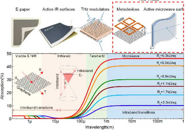
Graphene is a new candidate for an active material to investigate light matter interactions. Monoatomic thickness, linear band structure, high mobility charge carriers together with the electrical tunability are the key physical properties that make graphene unique to control electromagnetic waves in a very broad spectrum. This broad optical response originates from interband and intraband electronic transitions. In visible and near infrared frequencies, interband transitions yields a universally constant optical conductivity of 𝜎 = 𝑒2/4ℏ where 𝑒 is the charge of
electron and ℏ is Planck’s constant. As a consequence of that graphene can absorb at most ~2.24% of the incident radiation (Figure 1.1) [1]. This broadband constant optical conductivity can be blocked by doping. When the Fermi energy of graphene is above half of the incident radiation energy, Pauli blocking suppresses the interband transitions hence graphene becomes transparent below that energy. For long wavelengths, from far infrared to microwave region, graphene has a frequency dependent optical conductivity of 𝜎(𝜔) = 𝜎0/(1 − 𝑖𝜔𝜏) due to the dominant
intraband transitions where 𝜔 is frequency and 𝜏 is scattering time. For this regime, the optical conductivity of graphene is due to intraband transitions and it can be enhanced by doping. In the free standing form, doped graphene can absorb at most 50% of incident radiation when the impedance of the graphene matches the half
2
of free space impedance (377𝛺) (Figure 1.1). This significant amount of absorption can be tuned by varying the charge density of graphene (Figure 1.1). This tunable optical absorption over a broad spectrum makes graphene a unique material for optoelectronic applications. Figure 1 summaries some possible applications based on tunable optical absorption of single layer graphene.
Figure 1.1 Graphene based optoelectronic devices working in various wavelengths investigated by our group. The highlighted devices in the microwave regime are investigated during my Ph.D. study. This thesis will describe the fabrication and characterization of these devices. The graph shows the calculated optical absorption of single layer graphene which yields controllable optical absorption in a very broad electromagnetic spectrum. Although the amount of absorption in visible and infrared wavelengths is small, especially for the long wavelength region tunability is as high as 50%.
3
Although the main stream graphene research is focused on electronic applications, recently, there has been various device structures investigated to tune the optical properties of graphene from visible to terahertz frequencies. Feng Wang et al. develops a gate tunable absorption in infrared for the first time [2] and Li et al. investigated the optical properties of graphene by varying conductivity of graphene again in the infrared [3]. Ming Liu et al. developed a broadband electro optical modulator mounted on top of a waveguide working in near-infrared wavelengths [4]. Polat et al. investigated for the first time a broadband graphene modulator working in the visible and near-infrared by using self-gated graphene supercapacitors [5] and they improved the method for the multilayer graphene modulators to increase the modulation performance of the device [6]. Rodriguez et al. investigated broadband graphene terahertz modulators and absorbers [7, 8]. Further, Kakenov et al. developed high performance terahertz spatial light modulators using self-gating device structure [9]. Graphene modulators were integrated also with terahertz metamaterials to tune amplitude and frequency of the metamaterials [10-14]. The optical properties of graphene for the visible and infrared region have been investigated in detail. However, the microwave region of the electromagnetic spectrum has not been investigated due the long wavelength and requirement of large area graphene devices. This thesis aims to bridge this gap by overcoming the challenging growth and fabrication processes for active microwave devices. Our strategy is to synthesize large area graphene samples using chemical vapor deposition and to develop transfer printing technique. After achieving high quality graphene samples, we fabricated large area active graphene devices using self-gated supercapacitor structures. Self-gated graphene supercapacitors provides a homogenous doping over a large surface area. In this thesis I will describe the details of the growth, fabrication, and characterization of these devices.
4
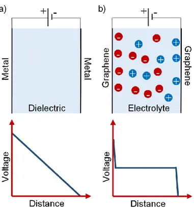
Figure 1.2 Comparison of (a) a dielectric capacitor and (b) a graphene supercapacitor.
Using graphene supercapacitors to control microwaves is the core idea of this thesis. Supercapacitor structure yields a self-gating scheme between two large area graphene. Self-gating with an ionic liquid electrolyte is the key parameter to achieve large and homogenous modulation of charge density over large area. Our group has been working on graphene supercapacitors based on single- and multi-layer graphene to control various wavelength (schematics in Figure 1.1). We would like to use graphene supercapacitors as a reconfigurable surface for microwave applications. We fabricated these supercapacitors (sometimes called electrical double layer capacitors) using large area graphene electrodes synthesized by chemical vapor deposition. A conventional dielectric-based capacitor uses two metal electrodes and a dielectric medium. Applied voltage between the electrodes generates homogeneous electric field between the plates and thus the voltage drops linearly on the dielectric.
5
Supercapacitors are different. Supercapacitors consist of two electrodes and electrolyte medium. Applied voltage polarizes the electrolyte and forms ionic double layers on the electrode surface. The thickness of these ionic double layers is very thin (a few nanometers limited by the diffusion of ions), therefore applied voltage drops sharply at the ionic double layer and generates very large electric field on the surface of electrodes (Figure 1.2(b)). We will use graphene supercapacitors where the electrodes are atomically thin graphene layers. As an electrolyte we will use ionic liquids which yield very good electrochemical stability with graphene electrodes up to 7 V electrochemical window. The electric field of the ionic double layers electrostatically dopes the graphene electrodes and accumulates charges. Unlike metallic electrodes, conductivity of atomically thin graphene electrodes varies with accumulated charges. The ability of tuning charge density on graphene electrodes yields a unique opportunity to control high mobility free charges on graphene surfaces. The maximum resistivity is reached at the Dirac point, where Fermi energy is the intersection point of the conduction and valance band. For the doped case, the charge density on graphene electrodes could be as large as 1014 cm-2 with associated
Fermi energy of 1.5 eV. These charge densities cannot be achieved with conventional dielectric capacitor due to the dielectric breakdown. Another important property of the supercapacitors is that they store charges at the graphene-electrolyte interface. There is no electrochemical reaction (which is the case for batteries) that can yield detrimental effects on graphene electrodes.
6
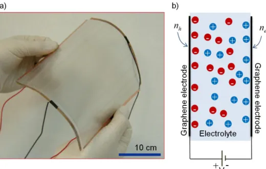
Figure 1.3 The photograph of large area graphene supercapacitor (a) and schematic explanation of ionic gating of graphene electrodes by an ionic liquid (b).
In this thesis, we use large area graphene supercapacitors (Figure 1.3) for the first time to control electromagnetic waves in the microwave frequencies. We have developed three different kinds of device structures. First one is a transmission type broadband microwave modulator fabricated by using two large area graphene electrodes with an ionic liquid between them. This device tunes the reflection, transmission, and absorption of microwaves from the surface of the device by applying bias voltage between two graphene electrodes. Second one is a reflection type radar absorbing surface. Here we use a large area graphene supercapacitor with a metal plate located at quarter wavelength distance below the device. This reflection type surface attenuates the reflected radiation at the resonance frequency. Our third device is achieved by integrating a large area graphene supercapacitor with a split ring resonator (SRR) array. Graphene capacitor is capacitively coupled with the SRR array, tuning the charge density on the graphene electrodes tunes the resonance amplitude and frequency of the hybrid metadevice.
7
Before going through the details of these active modulators, I will first introduce the fundamentals of graphene in this chapter which covers the electronic band structure and optical conductivity. In chapter 2, I calculate optical absorption of graphene in whole non-ionizing electromagnetic spectrum by solving Maxwell equations on graphene surface and I use a transfer matrix method for numerical calculation. In chapter 3, I explain the details of graphene synthesis and characterization and then we express the details for the fabrication of large area graphene capacitors with characterization processes. In chapter 4, I explain the performance and characteristics of transmission type adaptive microwave surfaces and reflection type switchable radar absorbing surfaces. In chapter 5, I report an application for our method. I integrated our active devices with microwave metamaterials and realized large area electrically switchable metadevices. I also provide electromagnetic modelling, fabrication and microwave measurements of these metadevices.
1.1.Electronic band structure of graphene
Graphene is the 2D crystal of carbon, each atom is bonded to three carbon atoms and forms a hexagonal atomic structure as shown in Figure 1.4. Carbon atom has different bonding mechanism when it is in a ground state[15]. In ground state, each carbon atom has six electrons and these electrons fill the energy levels of the carbon atom as 1𝑠22𝑠22𝑝2 where the 2𝑝2 state is partially filled as 2𝑝
𝑥12𝑝𝑦12𝑝𝑧0. The two electrons
in 1𝑠2 state are the core electrons and they do not contribute to chemical bonding or
electronic properties of the carbon atom. The four electrons in 2𝑠22𝑝2 states are called valance electrons and they define electronic properties of a carbon based materials. In its ground state a carbon atom can only make two bonds by using its two half-filled 2𝑝 orbitals as in 𝐶𝐻2. However, when a carbon atom is in the excited state, it can make four bonds by exiting one electron from 2𝑠 orbital to the a 2𝑝 orbital,
8
four half-filled electronic state give rise to more than two chemical bonds for a single carbon atom in a crystal. The energy difference between higher energy 2𝑠 orbitals and lower energy 2𝑝 orbitals is small compared to the chemical binding energies, therefore, the wave functions of electrons in these two energy orbitals are mixed. Hybridizations are when one electron from the 2𝑠 orbital hybridize with one(𝑠𝑝), two (𝑠𝑝2) or three(𝑠𝑝3) electrons from 2𝑝 orbitals. These hybridized electronic
states forms 𝜎 bonds with hydrogen atom or carbon atom itself and remaining half-filled 2𝑝 orbitals form the 𝜋 bonds between carbon atoms and they are perpendicular to the 𝜎 bonds.[15] This variety of hybridization results in a wide variety of carbon based materials.
In graphene, there is 𝑠𝑝2 hybridization, one of the electrons from 2𝑠 orbital
and two(2𝑝𝑥2𝑝𝑦) of electrons from 2𝑝 orbital mix their wave functions and they
hybridize in a new energy state as explained in Ref.[15] and Ref.[16]. These hybridized orbitals create strong 𝜎 bonds between a carbon atom and its three nearest neighbors, this strong bond gives rise to the stability of graphene in 2-dimension. Un-hybridized 2𝑝𝑧 orbital creates 𝜋 orbitals which are perpendicular to the graphene plane. 𝜋 Electrons are responsible for all transport and electronic structure of graphene and graphene based materials. Tight binding calculation of these 𝜋 electrons gives the electronic band structure of graphene, which means that the interaction between these electrons creates an energy-band diagram where energy-momentum combination of any charge carrier is defined by the band structure. To calculate electronic band structure of graphene, we need to know the crystal structure of graphene drawn schematically in Figure 1.4. In this hexagonal crystal structure of graphene, blue and red dots represent the carbon atoms in hexagonal graphene lattice. It is assumed that the red dots are the lattice points and the blue dots are the sub-lattice points. The sub-sub-lattice points are connected to the sub-lattice points by any one of 𝑏1,2,3
⃗⃗⃗⃗⃗⃗⃗⃗⃗ vectors as in Ref.[16]. The vectors 𝑎⃗⃗⃗⃗ and 𝑎1 ⃗⃗⃗⃗ are the lattice vectors of the 2
9 𝑎1 ⃗⃗⃗⃗ =𝑎 2(3, √3) , 𝑎⃗⃗⃗⃗ =2 𝑎 2(3, −√3) (1.1)
Where 𝑎 ≈ 1.42𝐴𝑜 is the distance between carbon atoms. The vectors 𝑏 1
⃗⃗⃗ , 𝑏⃗⃗⃗⃗ and 𝑏2 ⃗⃗⃗⃗ 3 show the first nearest neighbor position of the carbon atom at lattice point and they can be written in terms of lattice vectors as
𝑏1
⃗⃗⃗ =𝑎
2(1, √3) , 𝑏⃗⃗⃗⃗ =2 𝑎
2(1, −√3) , 𝑏⃗⃗⃗ = −𝑎(1,0) 1 (1.2)
It is possible to consider the second, third and higher order nearest neighbor interactions during calculation of the electronic band structure of graphene by tight binding method. However, it is not practical and necessary to consider higher order nearest neighbor interactions. Therefore, we calculated band structure of graphene by only considering the first nearest neighbor interactions as in Ref.[15].
Figure 1.4: Schematic drawing of hexagonal lattice structure of graphene. Red and blue dots represent the carbon atoms in graphene structure and red dots are assumed to be the lattice points for a triangular lattice. Blue dots are sub-lattices which are
connected to a lattice point with a basis vector. Here we assume any one of 𝑏⃗⃗⃗⃗⃗⃗⃗⃗⃗ 1,2,3
vectors as a basis vector. The vectors 𝑎⃗⃗⃗⃗ and 𝑎1 ⃗⃗⃗⃗ are lattice vectors and 𝑏2 ⃗⃗⃗ , 𝑏1 ⃗⃗⃗⃗ and 𝑏2 ⃗⃗⃗⃗ 3 are the vectors showing the nearest neighbor position of a carbon atom relative to a lattice point. The side length of a hexagon is 𝑎.
10
Graphene has 𝜋 electrons in its unit cell and the 𝜋 electrons determine the extraordinary electrical, optical and mechanical properties of graphene. Tight binding calculation takes account 𝜋 electrons to calculate band structure of graphene. In fact there are also 𝜎 electrons in the graphene unit cell but 𝜋 electrons are more dominant in low energy regimes. Therefore we only considered 𝜋 electrons during the calculation of band structure of graphene as in Ref.[15]. Graphene has a two dimensional atomic crystal structure and hence it has a unit cell. Therefore, graphene has a translational symmetry. The wave function in a unit cell satisfies the Bloch`s theorem;
𝑇𝑎⃗⃗⃗⃗ 𝑖𝛹 = 𝑒𝑖𝑘⃗ .𝑎⃗⃗⃗⃗ 𝑖𝛹 , (𝑖 = 1,2,3) (1.3)
Where 𝑇𝑎⃗⃗⃗⃗ 𝑖 is the translation operator and, 𝑎⃗⃗⃗ is the lattice vector and 𝑘𝑖 ⃗⃗⃗ is the wave 𝑖 vectors. 𝛹 is the wave function in a unit cell and has the form as
𝜑𝑗(𝑘⃗ , 𝑟 ) = 1 √𝑁∑ 𝑒 𝑖𝑘⃗ .𝑟 𝑁 𝑅⃗ 𝜑𝑗(𝑟 − 𝑅⃗ ) , (𝑗 = 1, … , 𝑛) (1.4) Where 𝜑𝑗 denotes the atomic wave function in a unit cell and 𝑅⃗ is the position of the atom in a unit cell, 𝑛 is the number of atoms in a unit cell. The eigenfunctions can be written as a linear combination of Bloch`s wave functions as
𝛹𝑗(𝑘⃗ , 𝑟 ) = ∑ 𝐶𝑖𝑗(𝑘⃗ )𝜑𝑖(𝑘⃗ , 𝑟 ) 𝑛
𝑖
(1.5)
Eigenvalues of these eigenfunctions can be calculated by evaluating the expectation value of Hamiltonian as
𝐸𝑗(𝑘⃗ ) =⟨𝛹𝑗|𝐻|𝛹𝑗⟩
⟨𝛹𝑗|𝛹𝑗⟩ (1.6)
By inserting the Bloch function from Eq.(1.4) in to Eq.(1.6), the transfer and overlap integral matrices can be calculated as
11
𝐻𝑖𝑗(𝑘⃗ ) = ⟨𝜑𝑖|𝐻|𝜑𝑗⟩ , 𝑆𝑖𝑗(𝑘⃗ ) = ⟨𝜑𝑖|𝜑𝑗⟩ (𝑖, 𝑗 = 1, … , 𝑛). (1.7)
Here 𝑖, 𝑗 show the number of atoms in the unit cell, for example, the number of atoms in a unit cell of graphene is two, one is at lattice point and the other one is at 𝑏⃗⃗⃗ 1
position as shown in Figure 1.4 and Eq.(1.2). Let us assume that the atom at the lattice point is represented with 𝐴 and the other atom in the unit cell is represented with 𝐵. The calculation over atoms 𝐴 and 𝐵 only gives the orbital energy of the 2𝑝 orbital as shown below
𝐻𝐴𝐴= 𝐻𝐵𝐵 = 𝜀2𝑃 (1.8)
By considering only the first nearest neighbor interaction, we can calculate off-diagonal elements of Hamiltonian as
𝐻𝐴𝐵 = 𝑡 (𝑒𝑖𝑘⃗ .𝑏⃗⃗⃗⃗ 1+ 𝑒𝑖𝑘⃗ .𝑏⃗⃗⃗⃗ 2 + 𝑒𝑖𝑘⃗ .𝑏⃗⃗⃗⃗ 3) = 𝑡𝑓(𝑘) (1.9)
Where 𝑏⃗⃗⃗⃗⃗⃗⃗⃗⃗ are the position vectors of first nearest neighbors as shown in Figure 1.4 1,2,3
and Eq.(1.2). Using coordinates from Eq.(1.2), 𝑓(𝑘) is calculated as 𝑓(𝑘) = 𝑒𝑖𝑘𝑥𝑎+ 2𝑒−𝑖𝑘2𝑥𝑎cos (𝑘𝑦𝑎√3
2 ) (1.10)
The overlap integral values are calculated as 𝑆𝐴𝐴= 𝑆𝐵𝐵 = 1 and the off-diagonal terms are 𝑆𝐴𝐵 = 𝑆𝐵𝐴 = 𝑠𝑓(𝑘). Finally the transfer and overlap matrices become as
𝐻 = (𝑡𝑓(𝑘)𝜀2𝑝 ∗ 𝑡𝑓(𝑘)𝜀
2𝑝 ) , 𝑆 = (
1 𝑠𝑓(𝑘)
𝑠𝑓(𝑘)∗ 1 ) (1.11)
Eigen values are calculated by solving the secular equation det(𝐻 − 𝐸𝑆) = 0, which gives
𝐸±(𝑘⃗ ) =𝜀2𝑝 ± 𝑡𝑤(𝑘⃗ )
1 ± 𝑠𝑤(𝑘⃗ ) (1.12)
Where ± corresponds to the energy of conduction and valance bands, respectively. The function in Eq.(1.12) is
12 𝑤(𝑘⃗ ) = √1 + 4cos (3𝑘𝑥𝑎 2 ) cos ( 𝑘𝑦𝑎√3 2 ) + 4𝑐𝑜𝑠2( 𝑘𝑦𝑎√3 2 ) (1.13)
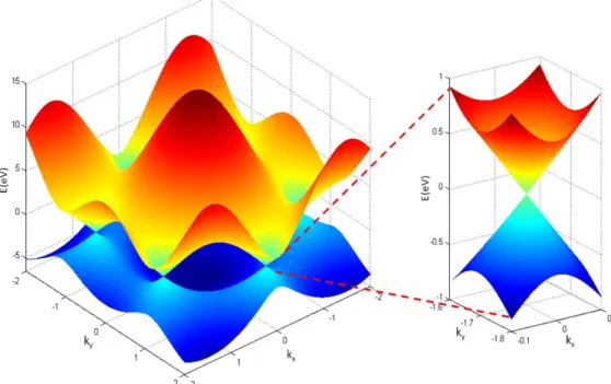
Calculated electronic band structure of graphene in the first Brillouin zone is shown on the left plot in Figure 1.5. At high energies, conduction band and valance bands are not degenerate. However, at lower energies near the Dirac points, conduction and valance bands are nearly degenerate and band structure is linear near the Dirac point as shown on the right plot in Figure 1.5. Near the Dirac point, energy of the electrons are linear with wave vector as 𝜀𝑐𝑣(𝑘) = ±𝑣𝑘 and the electrons have a constant
velocity 𝑣 = 106𝑚/𝑠. The velocity of electrons is 1% of the speed of light hence the
electrons of graphene mimic as relativistic like Dirac fermions near the 𝜀 = 0 regime.
Figure 1.5 Electronic band structure of graphene calculated using the tight binding method. The figure on the left shows the energies of the bands in the first Brillouin zone of graphene. Conduction and valance bands are not symmetric at higher energies but they are symmetric at lower energies near Dirac point as shown in the right plot. Here we used 𝜀2𝑝 = 0, 𝑡 = −3.033𝑒𝑉, and 𝑠 = 0.129 for the parameters in Eq.(1.12).
13
1.2.Optical Conductivity of graphene
Graphene is a zero band gap 2D crystal of carbon atoms arranged in a hexagonal lattice. Its conduction and valance bands meet at Dirac point where the density of states is zero. Away from the Dirac point, the density of states increases and number of allowed energy states increases as well. By chemical or electrostatic doping of graphene, Fermi level of the graphene moves towards or away from the Dirac point. In this way, charge density and conductivity of graphene are tuned. Graphene has a frequency dependent AC (𝜎𝑎𝑐) conductivity which converges to DC (𝜎𝑑𝑐)
conductivity at low frequencies. To calculate the DC conductivity of graphene in terms of its resistance, we first find the resistance of a 3D conductor. The resistance in 3D can be calculated from the 3D resistivity (𝜌3𝐷) of the conductor as
𝑅3𝐷 = 𝜌3𝐷
𝐿
𝐴 = 𝜌3𝐷 𝐿
𝑤𝑡 (1.14)
Where 𝐴 is the cross sectional area, 𝑤 is the width, 𝑡 is the thickness, 𝐿 is the length of the conductor. To find the resistance of the conductor in 2D, the 3D resistivity is converted to a 2D resistivity;
𝜌2𝐷= 𝜌3𝐷
𝑡 (1.15)
Where the unit of 3D resistivity is 𝛺. 𝑐𝑚. The unit of the 2D resistivity is 𝛺, this is actually misinterpreted with a total resistance hence the unit of 2D resistivity is written as 𝛺 𝑠𝑞⁄ . Then the total resistance of the 2D conductor is
𝑅2𝐷 = 𝜌2𝐷𝐿
𝑤 (1.16)
where the unit is in ohm (𝛺). For graphene, the resistance is represented mostly with the 2D resistivity as the sheet resistance 𝑅𝑠. The sheet resistance represents the
resistance of a square with any dimension. The sheet resistance should be the same for different sizes of graphene sheet with a square dimensions if the graphene sheet
14
is uniform. Resistivity is the inverse of the conductivity hence the DC conductivity can be expressed as 𝜎𝑑𝑐= 1 𝜌2𝐷 = 1 𝑅𝑠 (1.17)
Graphene has frequency dependent ac conductivity (𝜎𝑎𝑐) due to both
interband and intraband transitions. Interband transitions are the transition of electrons from valance band to conduction band initiated by absorbed energy of a photon. Electrons are Fermions and any of two electrons cannot be at the same energy and momentum state at the same time. An electron can transit from conduction band to valance band if the energy of incident photon is enough. If the corresponding energy level is already filled, then the Pauli blocking does not allow the electron to go that state. Therefore the optical conductivity of graphene strongly depends on the frequency of incident electromagnetic wave. There are number of methods as shown in Ref.[17],[18],[19] to calculate the optical conductivity of graphene due to interband transitions. We follow the method developed by Stauber et.al [19] to calculate the optical conductivity of graphene in visible and near infrared region of the electromagnetic spectrum. The derivation starts with Kubo formula which relates the average surface current density 〈𝑗𝑥𝐷〉, surface area 𝐴
𝑠 and a current correlation
function 𝛽;
𝜎(𝜔) = 〈𝑗𝑥𝐷〉
𝑖𝐴𝑠(𝜔 + 𝑖0+)+
𝛽(𝜔 + 𝑖0+)
𝑖ℏ𝐴𝑠(𝜔 + 𝑖0+) (1.18)
After a long and detailed calculation as given in Ref.[19], the interband conductivity of graphene can be expressed as
𝜎𝑖𝑛𝑡𝑒𝑟(𝜔) = 𝑒2 8ℏ[𝑡𝑎𝑛ℎ ( ℏ𝜔 + 2𝐸𝑓 4𝑘𝑏𝑇 ) + 𝑡𝑎𝑛ℎ ( ℏ𝜔 − 2𝐸𝑓 4𝑘𝑏𝑇 )] (1.19)
Where 𝐸𝑓 is the Fermi energy, 𝑘𝑏 is the Boltzmann constant, 𝑇 is the temperature. It
15
energy. And a small contribution to interband conductivity of graphene from the second nearest neighbor atoms in graphene lattice is also neglected.
Figure 1.6 Optical conductivity of graphene due to interband transitions with varying Fermi energies (a) and with varying temperatures (b). Graphene has a constant optical conductivity in a broad spectrum when the Fermi energy coincides with Dirac point. If the Fermi energy is shifted up or down to the Dirac point by chemical or electrical doping, optical conductivity of graphene goes down to zero for energies lower than two times the Fermi energy due to Pauli blocking of transitions from valance band to conduction band. Optical conductivity of graphene depends on the temperature. Electrons obey Fermi-Dirac statistics, therefore the behavior of Pauli blocking is sharp at low temperatures. Due to thermal fluctuations, the step function due to Pauli blocking becomes broader as temperature increases.
16
The first term in Eq.(1.19) can be expressed in terms of the universal conductivity of graphene as[20],[21]
𝜎0(𝜔) = 𝑒2
4ℏ= 60.8𝜇𝑆 (1.20)
This is the universal conductivity of an un-doped graphene due to interband transitions, and the conductivity does not depend on any microscopic parameters. As shown in Figure 1.6(a), if the Fermi level of graphene is at the Dirac point, optical conductivity of graphene is constant and corresponds to the universal optical conductivity of 𝑒2/4ℏ in a broad optical spectrum. When the Fermi level of graphene
is shifted up or down to the Dirac point, optical transitions between valance and conduction bands are blocked due to the Pauli blocking. Therefore, optical conductivity of graphene goes down to zero for optical energies less than two times the Fermi energy of graphene. Interband conductivity of graphene also depends on the temperature as shown in Figure 1.6(b). At low temperatures, electrons of graphene strongly obey the Fermi-Dirac statistics. Therefore the transition from allowed energy states to the forbidden energy states is sharp at the optical energy that equals to two times the Fermi energy of graphene. At high temperatures, the transition from allowed energy states to the forbidden energy states is not very sharp due to thermal fluctuations.
In order to calculate the ac conductivity of graphene due to the intraband transitions, we follow the calculation performed in [17]. The intraband conductivity of graphene is given by the following equation
𝜎𝑖𝑛𝑡𝑟𝑎(𝜔) =𝑒2𝜔 𝑖𝜋ℏ∫ 𝑑𝜀 |𝜀| 𝜔2 +∞ −∞ 𝑑𝑓0(𝜀) 𝑑𝜀 (1.21)
Where 𝑓0(𝜀)is the Fermi-Dirac distribution function given by
𝑓0(𝜀) = (𝑒(𝜀−𝜇)𝑇 + 1) −1
17
Where 𝜇 is the chemical potential, 𝑇 is the temperature. If we integrate (1.21) by inserting 𝑓0(𝜀) from (1.22), intraband conductivity can be calculated as
𝜎𝑖𝑛𝑡𝑟𝑎(𝜔) =2𝑖𝑒2𝑇
𝜋ℏ𝜔 𝑙𝑛 [2cosh ( 𝜇
2𝑇)] (1.23)
Electrons in the filled energy states of graphene behave like free electrons similar to electrons in metals, hence, intraband transitions of electrons in graphene can be explained by using the Drude model. It is assumed that an electrons move like a free electron between scattering events in Drude model. The average time between two scatterings of electron is called relaxation time to be 𝜏 and the scattering rate is 𝛤 = 1/𝜏. In order to insert scattering rate into Eq.(1.23), the frequency is expressed as 𝜔 = (𝜔 + 𝑖𝛤), therefore,
𝜎𝑖𝑛𝑡𝑟𝑎(𝜔) = 2𝑖𝑒2𝑇
𝜋ℏ(𝜔 + 𝑖𝛤)𝑙𝑛 [2cosh ( 𝜇
2𝑇)] (1.24)
In the Fermi-Dirac statistics, it is assumed that for 𝜇 ≫ 𝑇, the last term in Eq.(1.24) becomes
𝑙𝑛 [2cosh (𝜇 2𝑇)] =
|𝜇|
2𝑇 (1.25)
After inserting Eq.(1.25) in to Eq.(1.24), then
𝜎𝑖𝑛𝑡𝑟𝑎(𝜔) = 𝑖𝑒2|𝜇| 𝜋ℏ(𝜔 + 𝑖𝛤) (1.26) If we assume |𝜇| ≈ 𝐸𝑓, then 𝜎𝑖𝑛𝑡𝑟𝑎(𝜔) =𝑒2𝐸𝑓𝜏 𝜋ℏ 1 (1 − 𝑖𝜔𝜏) (1.27)
This is the same form of conductivity which is calculated for metals by using the Drude model. AC conductivity of a metal is given as 𝜎(𝜔) = 𝜎0/(1 − 𝑖𝜔𝜏) where 𝜎0 is the DC conductivity of the metal. As a result, we can clearly determine that the
18
𝜎𝐷𝐶 = 𝑒2𝐸𝑓𝜏⁄ , 𝜋ℏ (1.28)
Then,
𝜎𝑖𝑛𝑡𝑟𝑎(𝜔) = 𝜎𝐷𝐶
(1 − 𝑖𝜔𝜏) (1.29)
We have also calculated DC conductivity of graphene by using sheet resistance of graphene in Eq.(1.17). If we insert Eq.(1.17) into Eq.(1.29), then the intraband AC conductivity of graphene can be expressed in terms of DC conductivity as
𝜎𝑖𝑛𝑡𝑟𝑎(𝜔) = 1
𝑅𝑠(1 − 𝑖𝜔𝜏) (1.30)
In addition, we can find a relation between the sheet resistance (𝑅𝑠) of graphene and its Fermi energy by using Eq.(1.28) and Eq.(1.17) as
𝑅𝑠𝐸𝑓 = 𝜋ℏ
𝑒2𝜏 ≈ 0.334 𝑘𝛺. 𝑒𝑉 (1.31)
Where we assume 𝜏 = 160𝑓𝑠 which is experimentally measured scattering time of CVD grown graphene [22].
We plot the intraband conductivity of graphene from 1𝜇𝑚 to 1𝑚 wavelength range in the unit of universal conductivity (𝑒2/4ℏ) of graphene (Figure 1.7). When
the Fermi energy of graphene is at the Dirac point, the valance band is completely filled and the conduction band is empty. Therefore, there is no available intraband transition states for electrons to be excited. As a result, the intraband conductivity of graphene is zero for all wavelength for 0𝑒𝑉 Fermi energies. When the Fermi level is shifted up or down of the Dirac point via electrostatic doping, there are available intraband energy states for electrons to be excited with a small amount of optical energies. When an electron in the conduction band of graphene is excited to an intraband energy state in the same band by a small optical energy, that electron transits to the available states above the Fermi level in the same band and relax back its initial energy level. Similar case happens for holes in the valance band, but in the opposite direction. Intraband conductivity of graphene is zero when 𝐸𝑓= 0𝑒𝑉 as
19
shown in Figure 1.7, however, it increases as the Fermi energy of graphene goes to 𝐸𝑓 = 3𝑒𝑉. Experimentally accessible the highest Fermi level is 𝐸𝑓 ≈ 1𝑒𝑉 [5].
Figure 1.7 Intraband conductivity of graphene for various Fermi level energies of graphene in the unit of universal conductivity of graphene. When Fermi level of graphene is at Dirac point, there is no electron in the conduction and no holes in the valance bands, and therefore, intraband conductivity of graphene is zero. If the Fermi level of graphene is in the conduction or valance band, then there are filled energy levels in graphene and intraband conductivity of graphene is nonzero. Intraband conductivity of graphene increases with an increase in the Fermi energy of graphene.