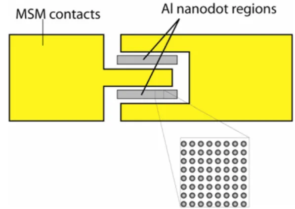
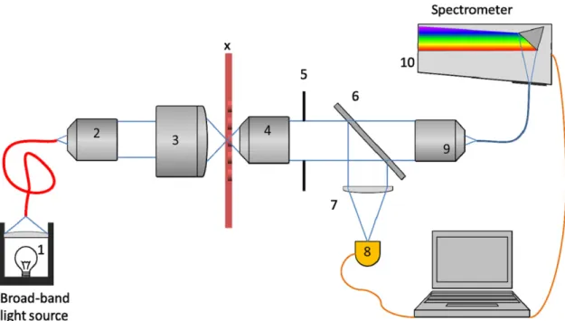
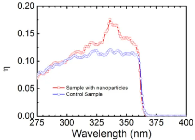
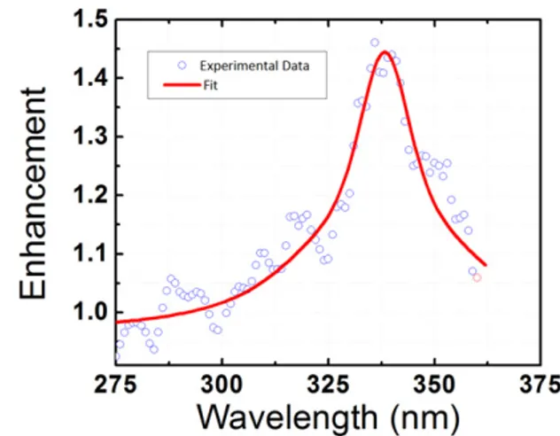
LSPR enhanced MSM UV photodetectors
Tam metin
Şekil
Benzer Belgeler
Overton’a göre, aldatmanın, hem kadın hem de erkek açısından yasal olarak suç sayıldığı, ancak kadın ve erkeğe verilen cezalar bakımından bir çifte standardın söz
Bakteriler, linoleik asidi hidrojenize etmekte ve bu reaksiyonda bafll›ca ürün olarak trans 11, C 18:1 (vaksenik asit) ya¤ asidini temel substrat olarak kullan›p son ürün
Gazi Üniversitesi, 1 Gazi Eğitim Fakültesi, 2 Tıp Fakültesi, Sağlık Araştırma ve Uygulama Merkezi, 4 Eczacılık Fakültesi, Biyokimya Anabilim Dalı, 14 Diş
Sonuç olarak, açımlayıcı ve doğrulayıcı faktör analizi sonucunda elde edilen değerler, BÖAÖ’nün lise öğrencilerinin biyoloji öğrenme anlayışlarını
Deneysel çalışmalarda kullanılmak üzere üretilen balatalardan TS 9076'ya göre hazırlanan numunelerin TS 555 kapsamında sürtünme katsayısı, sürtünme esnasında
More specifically, if all motion vectors are forward motion vectors, then the current B frame is a scene cut because the previous frame is significantly irrelevant to the
The results of this study show that texture analysis can be used to quantify variations in voxel intensities over time, and can be used along with a neural network to segment
In computer networks RTT is probably time varying or uncertain and for better performance, in [26], switching among a set of robust controllers was proposed. In this section we use
