I
PHOTO-DYNAMIC XPS FOR INVESTIGATING PHOTOINDUCED
VOLTAGE CHANGES IN SEMICONDUCTING MATERIALS
A DISSERTATION SUBMITTED TO THE DEPARTMENT OF CHEMISTRY
AND THE GRADUATE SCHOOL OF ENGINEERING AND SCIENCE OF BILKENT UNIVERSITY
IN PARTIAL FULFILLMENT OF THE REQUIREMENTS FOR THE DEGREE OF
DOCTOR OF PHILOSOPHY
By
HİKMET SEZEN December, 2011
II
I certify that I have read this thesis and that in my opinion is it is fully adequate, in scope and in quality, as a dissertation for the degree of the doctor of philosophy,
……….. Prof. Dr. Şefik Süzer (Principal Advisor)
I certify that I have read this thesis and that in my opinion is it is fully adequate, in scope and in quality, as a dissertation for the degree of the doctor of philosophy,
……….. Prof. Dr. O. Yavuz Ataman
I certify that I have read this thesis and that in my opinion is it is fully adequate, in scope and in quality, as a dissertation for the degree of the doctor of philosophy,
……….. Prof. Dr. Ekmel Özbay
III
I certify that I have read this thesis and that in my opinion is it is fully adequate, in scope and in quality, as a dissertation for the degree of the doctor of philosophy,
……….. Assoc. Prof. Dr. Oğuz Gülseren
I certify that I have read this thesis and that in my opinion is it is fully adequate, in scope and in quality, as a dissertation for the degree of the doctor of philosophy,
……….. Assist. Prof. Dr. Emrah Özensoy
Approved for the Graduate School of Engineering and Science:
……….. Prof. Dr. Levent Onural (Director of the Institute)
IV ABSTRACT
PHOTO-DYNAMIC XPS FOR INVESTIGATING PHOTOINDUCED
VOLTAGE CHANGES IN SEMICONDUCTING MATERIALS
HİKMET SEZEN Ph.D. in Chemistry
Supervisor: Prof. Dr. Şefik Süzer December, 2011
The main motivation of this Ph.D. study is investigation of the photoinduced voltage changes in semiconductive materials with X-ray Photoelectron Spectroscopy (XPS). For this purpose, we have developed a technique for recording the shifts in the positions of the XPS peaks in response to different waveforms of electrical and/or optical stimuli for tracing dynamics of the developed potentials originating from intrinsic or extrinsic factors of the semiconductive materials such as charging/discharging, photoconductivity, surface photovoltage, band-bending/flattening/inversion, etc.
Within this purpose, the surface photovoltage behaviors of n- and p-type doped Si and GaN samples are examined with the photo-dynamic XPS, to follow the behavior of the band-bending under photoillumination in both static and dynamic fashions. The band inversion effects are clearly observed on the n- and p-Si samples in the presence of a dielectric silica overlayer and on the p-GaN sample due to variation of the illuminating laser energies.
V
Moreover, the extent of the dopant dependent XPS peak shifts of the n- and p-Si samples are assessed after correction of their surface photovoltage values.
A laser patterned silicon wafer with a high-power near infrared fiber laser is also investigated. While the patterned silica domains have identical chemical composition with the non-patterned regions, an investigation with dynamic XPS clearly reveals distinct dielectric characteristics of the patterned domains.
Electrical parameters of CdS thin film are extracted by dynamic XPS with and without photoillumination. The photo-dynamic XPS technique has also provided useful information by disentanglement of processes; charging/discharging, photoconductivity, and surface photovoltage. Furthermore, location (space) dependent resistance and chemical profile of a CdS based Light Dependent Resistor (LDR) is also probed during realistic operational conditions, by utilizing spatially resolved XPS analysis (in the area mapping mode). In addition, with the XPS mapping analysis defects and malfunctioning sites/domains have been located under various experimental and preparation conditions.
Keywords: XPS, Dynamic XPS, Photo-Dynamic XPS, Charging, Discharging, Charge
Contrast, Photoconductivity, Surface Photovoltage, Band-Bending, Band-Flattening, and Band-Inversion, Laser Patterning, Light Dependent Photoresistor.
VI ÖZET
IŞIK ALTINDA YARIİLETKEN MALZEMELERİN ÜZERİNDE
OLUŞAN VOLTAJ YÜKLENMELERİNİN FOTO-DİNAMİK XPS İLE
İNCELENMESİ
HİKMET SEZEN Kimya Doktora Tezi Danışman: Prof. Dr. Şefik Süzer
Aralık, 2011
Bu doktora tezinin temel amacı, ışık uyarılmaları altında, yarıiletken malzemeler üzerinde meydana gelen voltaj yüklenmelerinin X-ışını fotoelektron spektroskopisi (XPS) ile incelenmesidir. Öncelikle malzemeleri değişik şekil ve hızlarda hem elektriksel hem de ışıksal olarak uyarabileceğimiz, aynı zamanda yarıiletken malzemelerin içsel ve dışsal özelliklerine bağlı olarak meydana gelebilecek potansiyel değişimlerini takip edebileceğimiz yeni bir teknik olan foto-dinamik XPS tekniğini geliştirdik.
Bu amaç dogrultusunda, hem n- ve p-Si hem de n- ve p-GaN numunelerinin yüzey fotovoltaj davranışları, yüzey bant düzlenmeleri statik ve dinamik ışık uyarımları yardımı ile XPS kullanılarak takip edildi. Ayrıca, yarıiletkenler üzerinde bant ters-eğrilme etkileri n- ve p-Si için ince bir silika tabakası oluşturulduğu zaman, ayrıca p-GaN için farklı dalga boylarında bulunan ışıklar ile uyarıldığı süreçlerde gözlemlendi. Ek olarak, bu teknik ile silikon numunelerindeki eser miktarda eklenmiş bulunan elementler vasıtasıyla ortaya çıkan enerji
VII
kaymalarının yüzey fotovoltaj değerleri ile düzeltildikten sonra foto-dinamik XPS tekniğini kullanarak takip edilebileceğini gösterdik.
Yüksek yoğunluktaki kızılötesi lif lazer ile silikon üzerindeki desenlendirilmiş bölgeler XPS yardımı ile incelendi. Kimyasal içerik olarak, lazere maruz tutulan ve tutulmayan bölgeler arasında herhangi bir fark yok iken, dinamik XPS ile yaptığımız deneyler sayesinde lazer ile desenlendirilmiş bölgelerin kendine özgü dieletriksel özelliği olduğu gösterildi.
CdS filminin elektriksel özellikleri, ışık varlığında ve yokluğunda dinamik XPS kullanılarak ölçüldü. Ayrıca, foto-dinamik XPS tekniğinden, yüklenme, yük boşalması, fotoiletkenlik ve yüzey fotovoltaj gibi etkileri birbirlerinden ayırmada etkin bir şekilde yararlanılabileceği gösterildi. Ek olarak, CdS içeren bir fotoselin konuma bağımlı direnç ve kimyasal analizleri alan haritalamalı XPS ile ölçülmüştür. İlaveten, alan haritalamalı XPS kusurlu veya hatalı bölgelerin farklı koşullar altında ortaya çıkması ve bu farklı bölgeler arasında karşılaştırmalar yapabilmemizi sağladı.
Anahtar Kelimeler: XPS, Dinamik XPS, Foto-Dinamik XPS, Yüklenme, Yük Boşalması, Yük Ayrışımı, Fotoiletkenlik, Yüzey Fotovoltaj, Bant Eğrilmesi, Bant Düzelmesi, Bant Ters-Eğrilmesi, Lazer, Laser Desenlendirme, Işığa Bağımlı Direnç (Fotosel).
VIII
LIST OF ABBREVATIONS
XPS: X-Ray Photoelectron Spectroscopy UHV: Ultra High Vacuum
BE: Binding Energy KE: Kinetic Energy eV: Electron-Volt
hυ: Kinetic Energy of Photon
Ф: Work Function FWHM: Full With Half Maximum
AL: Attenuation Length
IMFP: Inelastic Mean Free Path
I: Electric Current or Intensity of Light Ix-ray: X-rays Induced Current
Ifil: Flood Gun Induced Current DC: Direct Current
SQW: Squarewave ZPC: Zero Point Charge
B.E. Diff.: Binding Energy Difference V: Electric Potential
R: Resistance or Resistor
Rph: Photoresistance or Photoresistor C: Capacitance or Capacitor
RC: Parallel Connected Resistor and Capacitor unit FG: Flood Gun or Function Generator
VCCS: Voltage Controlled Current Source σ: Conductivity
SPV: Surface Photovoltage a.u.: Arbitrary Unit
KP: Kelvin Probe NIR: Near Infrared CW: Continuous Wave
IX Ei: Intrinsic Fermi level
Ef: Fermi level VB: Valance Band CB: Conduction Band NDF: Neutral Density Filter OD: Optical Density
LDR: Light Dependent Resistor
Rsb: Electron Excitation from Surface to Bulk Rbs: Electron Excitation from Bulk to Surface TC: Time Constant
X
ACKNOWLEDGEMENTS
This short, but comprehensively scientific survey is more than achieving my Ph.D. degree, but is an enjoyable period of my life, and an impressive preface of my academic carrier. The most probable reason is the great interaction with my supervisor, Prof. Dr. Şefik Süzer, for the whole duration. I am aware of the privilege of working with my supervisor, and so I express my deepest thankfulness to him.
I would also like to convey my deepest thanks to Dr. Gülay Ertaş, who also supervised me during each step of my work. I thank to Prof. Dr. Mehmet Erbudak, Prof. Dr. Ekmel Özbay, Prof. Dr. Atilla Aydınlı, Assist. Prof. Dr. Ömer İlday, Assist. Prof. Dr. Özgür Aktaş, Assist. Prof. Dr. Özgür Birer, and Assoc. Prof. Dr. Oğuz Gülseren, who have significant roles in completion of my thesis. In addition, I also thank to Dr. Tim Nunney, Dr. Kevin S Robinson, and members of Surface Analysis Department of the ThermoFisher Co., UK, for their patience and kindness to our endless requests about the K-Alpha instrument.
Thanks also to current and previous Süzer-lab members; Merve Taner, Eda Yılmaz (Özkaraoğlu), Pınar Cönger, İlknur Kaya Tunç, Hacı Osman Güvenç, Sinem Yılmaz, Sevnur Kömürlü, Korcan Demirok, Bora İnci, Ferdi Karadaş, and Engin Karabudak.
I would like to express my appreciations to my dear friends for moral support without any remuneration; Cemal Albayrak, Mustafa Fatih Genişel, Yurdanur Türker, Emre Emmez and Emrah Parmak. Also special thanks to Ethem Anber, Emine Yiğit, Hüsnü İçer, and Bülent Öktem.
I always feel myself indebted to Bilkent University and Chemistry Department for providing a high level education and research opportunity.
Finally, I want to express my deepest gratitude to my family and my love Feriza Sezen if I could.
XI
Table of Contents
ABSTRACT……….... IV ÖZET………... VI LIST OF ABBREVATIONS………... VIII ACKNOWLEDGEMENTS……… X Table of Contents……… XI LIST OF FIGURES………. XIII LIST OF TABLE….……….……. XVIII
1. Introduction ...1
1.1. X-Ray Photoelectron Spectroscopy ... 1
1.1.1. Controlled Surface Charging ... 9
1.2. Photoconductivity ... 14
1.3. Surface Photovoltage ... 17
2. Aim of Work ...22
3. Experimental ...24
3.1. Sample Preparation ... 24
3.2. Instruments and Technique ... 27
3.2.1. Method and Model of Photo-Dynamic XPS ... 30
4. Results and Discussion ...37
4.1. Surface Photovoltage and Band Offset Measurements on n- and p-type Si ... 37
4.1.1. Inversion of the Surface Photovoltage of SiOx / n- and p-doped Si ... 45
4.1.2. Dynamical Photoconductivity and Surface Photovoltage Response of a SiOx / p-type Si Surface Structure ... 48
4.1.3. Elemental, Chemical, and Electrical Investigation of a High-Power Fiber Laser Patterned Silicon ... 51
XII
4.2. Photoresponse and Electrical Parameters of CdS Film ... 58
4.2.1. An XPS Investigation of CdS Based Photoresistor under Realistic Operational Conditions ... 64
4.3. Surface Photoresponse and Transients of n- and p-type GaN ... 77
4.3.1. Inversion of the Surface Photovoltage of p-type GaN ... 86
5. Conclusions ...88
XIII
LIST OF FIGURES
Figure 1. Basic principles and components of XPS experimental setup. ... 3 Figure 2. Schematic representation of the photoelectric effect. ... 4 Figure 3. (a) Photoelectric effect due to x-ray radiation and elastic and inelastic collision of
photoelectron (b) Beer-Lambert’s relation and depth profile of XPS with calculated values of corresponding intensity distribution from first three attenuation lengths. . 6 Figure 4. Charging processes in (a) a conductive and (b) a nonconductive material during
recording of XPS data. ... 10 Figure 5. (a) XPS spectra of the Si2p region of a SiO2/p-Si sample connected to ground
(green) and to +10 V(red) and – 10 V (blue) external DC stresses. The thickness of the silica overlayer is ca. 4 nm. (b) The variation of the current passing through the sample under various bias potentials. The inset on the top right depicts the experimental setup. ... 12 Figure 6. XPS spectra of the Au4f region, when the metal is connected externally to; (a)
ground; (b) SQW excitation of ±10.00 amplitude and at frequencies of 10 kHz (navy spectrum) and 0.001 Hz (magenta spectrum). The same spectra are reproduced after connecting to an external circuit, consisting of; (c) a series resistor (R=220 kΩ); (d) a series resistor and a parallel capacitor (R=220 kΩ, C=500 nF). A schematic diagram of the experimental set-up is given as an inset, where IX-ray
represents the electron current due to photo and secondary electrons generated, and IFlood is the current due to the flood-gun used. ... 14
Figure 7. Photoinduced electron-hole generation and separation in between n- and p-type semiconductor. ... 16 Figure 8. The band diagram of n-Si (a) in dark (b) under photoillumination and (c) in flattened
conditions. Adapted from the references 57, 58, 59, and 60. ... 18 Figure 9. The representative Si lattice structures of the n- and p-type doped with (a) P (b) B
elements. Adapted from the references 55 and 56. ... 20 Figure 10. (a) The XPS spectra and (b) band diagram of n- and p-type doped Si without and
with exciting light source (violet laser). While the left panel belongs to n-type Si, the right panel belongs to p-type Si. The dotted green circular and line indicates
XIV
effect of light source onto both band diagram and XPS spectra of n- and p- type doped Si.79 ... 21 Figure 11. The arrangement of experimental setup of the K-Alpha instrument. ... 28 Figure 12. The method of the photo-dynamic XPS. ... 32 Figure 13. The snapshot frames of spots of violet, green, red, and NIR lasers. The frames are
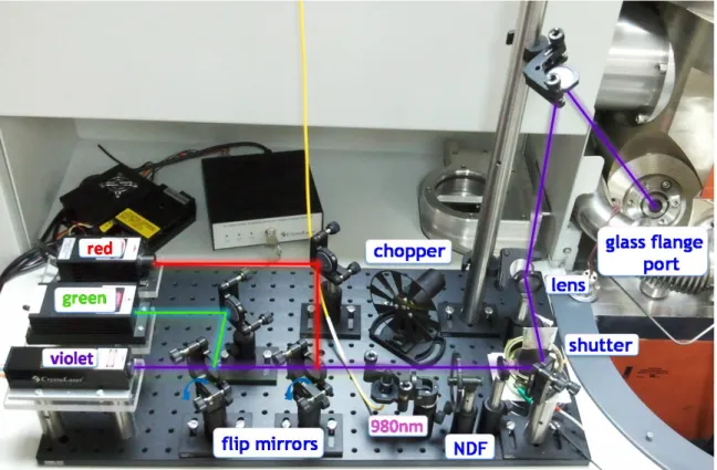
captured with the digital camera of K-Alpha. ... 33 Figure 14. The optical breadboard and other optic component of photo-dynamic XPS system.
The most of components are labelled and the pathes of laser beams are represented by properly colored lines. ... 35 Figure 15. The model of the photo-dynamic XPS. ... 36 Figure 16. The XPS spectra of Si2p regions of (a) n- (b) p-type doped Si without and with
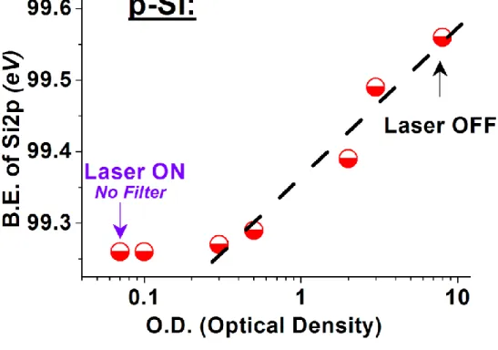
violet, green, red and near infrared laser excitations. ... 38 Figure 17. The response of peak position of p-type doped Si under exposes of violet laser with
tuned photon intensities. ... 39 Figure 18. The picture of sample mounting with Au sheet for the photo-dynamic XPS
measurement. ... 41 Figure 19. The band diagram of an (a) intrinsic (b) 2.8 x 1014 cm-3 of n-type and (c) 4.7 x 1014 cm-3 of p-type doped Si. ... 43 Figure 20. The band offset between n- and p-type doped Si (a) calculated, and (b) measured by
XPS without light illumination. ... 44 Figure 21. The experimental and fitted XPS spectra of Si2p regions of mechanically connected
n- and p- type Si (a) without and (b) with laser illumination. While the dotted points represent experimental data, solid lines represent fit Si2p spectra of n- and p-type Si samples. Inset shows a simple model of experimental setup. ... 44 Figure 22. The Si2p XPS spectra of (a) n-, (b) p-Si of HF cleaned Si wafers. The Si2p (c,d)
and O1s (e,f) spectra of n- and p-Si wafers which contain ca. 10 nm a thermal oxidized overlayers. ... 46 Figure 23. The corresponding surface photovoltage behaviors of (a) n- and (b) p-Si wafers
which contain ca. 10nm thermal silica from Si2p peaks and under a chopped photo-excitation at 0.01 Hz rate. The first cycle of Laser ON states are indicated on the both two spectra. The upper inset configuration and composition of the n- and
XV
p-Si samples and the bottom inset shows a single frame of the XPS snapshot experiment form p-Si. ... 47 Figure 24. A model of inversed surface photovoltage interface between the silica overlayers
and (a) n-, and (b) p-Si. ... 47 Figure 25. The XPS spectra of Si2p regions of p-type doped Si (HF cleaned) with and without
light illumination and while connected to (a) ground, (b) 1 kHz, and (c) 0.001 Hz squarewave electrical stress. ... 49 Figure 26. The XPS spectra of Si2p regions of ca. 4 nm silica layer and p-type doped Si
substrate with and without light illumination and while connected to (a) 1 kHz (b) 0.001 Hz squarewave electrical stress. ... 51 Figure 27. The elemental XPS survey of the laser patterned Si (a) Si2p region and (b) O1s
region. The left panel of inset is an optical image of the sample and shows the analyzed features and the x-ray spot (green circle) on the sample. The right panel of the inset shows chemical compositional analysis between Si and O element of the analyzed region.125 ... 53 Figure 28. A XPS line scan of (a) Si2p (b) O1s region on the patterned Si. (c) the fitted peaks
lines of both Si2p and O1s peaks vs. positions.125 ... 54 Figure 29. A 2D false color contour map of the sequential snapshot O1s spectra of the laser
patterned Si under a triangle (±10 V) electrical stimulus at the 0.1 Hz frequency. The inset shows two O1s snapshot spectra under -10 V (left) and +10 V (right) bias.125 ... 56 Figure 30. The variation of snapshot spectra of the O1s peaks of two silica domain (a) vs. each
other and (b) the B.E. Diff. between them vs. the O1s peak of the first silica domain.125 ... 57 Figure 31. The XPS spectra of Cd3d5/2 of the CdS film without and with violet laser excitation.
Inset shows the responses of CdS to violet, green and red lasers. ... 59 Figure 32. The relationship between the photoconductivity of the CdS film and intensity of the
incident light beam of violet (violet dots) and green (green dots) lasers. The dot points are experimental data and dashed lines are linear fits. ... 61 Figure 33. XPS spectra of Cd3d peak of CdS film with and without photoilliminuation and at a
XVI
intensity of excition source is tuned with NDF. The inset shows the experimental setup. ... 62 Figure 34. The frequency dependence of (a) the measured and calculated B. E. Diff. and
FWHM values of CdS film under saquarewave electric stress between 104 and 0.001 Hz with and without photoillimuniation. Inset shows allined values of resistance and capacitance value for both two laser off and on states. ... 64 Figure 35. The XPS Survey spectra of (a) the conductive and (b) the photoconductive regions
of a CdS based LDR. The inset is an optical picture of the device and electrical connection.79 ... 66 Figure 36. XPS depth profiles of CdS based LDR from (a) the conductive and (b) the
photoconductive regions.79 ... 67 Figure 37. An electric circuit model of the experimental setup to simulate location depended
resistance behavior of a CdS semiconductor under realistic conditions.79 ... 68 Figure 38. A false contour color plot of XPS line scan spectra along both the conductive and
the photoconductive regions of the device at the (a) laser off, (b) laser on states. (c) The measured binding energy position along the line scan without and under violet, green, red, and near infrared lasers illumination. (d) The position of the XPS line scan on the actual device.79 ... 71 Figure 39. (a) The measured binding energy positions of Cd5/2 peak and (b) corresponding
calculated location depended resistance values along the XPS line scan.79 ... 72 Figure 40. A false contour color plot of XPS area mapped spectra of the LDR device with two
lateral space dimensions and one energy dimension.79 ... 73 Figure 41. X-ray photocurrent maps with two dimensional space resolved spectra at (a) 405.2
eV, (b) 411.1 eV, (c) a summation of the intensities at 405.2 and 411.1 eV and (d) at 400 eV.79 ... 74 Figure 42. Intentionally selected XPS snapshot spectra for comparison of x-rays photocurrent
at 400 eV binding energy.79 ... 75 Figure 43. The defect region analysis of XPS mapping. (a) A big area Laser OFF, (b) defect
specified small area scans Laser OFF state (c) NIR Laser ON, and (d) violet Laser ON with iso-energy line to emphasize energy steps (0.2eV).79 ... 76
XVII
Figure 44. Survey XPS spectrum of p-type GaN sample. Inset demostrates the experimental setup. ... 78 Figure 45. The XPS spectra of the (a) n- and (b) p-type GaN with and without
photoillumination. ... 78 Figure 46. The bended band diagrams and possible sub-band gap photoexcitation processes of
(a) n-GaN (b) p-GaN. ... 80 Figure 47. The relationship between measured binding energy variation or build-up of the
surface photovoltage of p-GaN and the intensity of excitation source.79 ... 81 Figure 48. XPS spectra of Ga3d peaks of the n- and p-GaN with and without
photoillimination, at (a) 10 kHz, and (b) 0.001 Hz squarewave electrical excitation.79 ... 82 Figure 49. Frequency dependence of (a) the measured binding energies and (b) binding energy
difference of the p-GaN under different squarewave electrical excitation frequencies with and without photoillumination.79 ... 82 Figure 50. The meaured binding energy changes recorded in transient mode of Ga2p3/2 peak of
(a) n- (b) p-GaN whit and without low energy electrons. ... 84 Figure 51. The exponential fitting of the laser on and off transients of the p-GaN. The inset
demonstrates possible slow and faster mechanisms of the electron accumulation and sweeping in and from the conduction band. ... 85 Figure 52. (a) The surface photoresponse of the p-GaN under violet, green, and red laser
illumination and possible mechanisms of (b) inversion of the surface photovoltage of p-GaN for green and red laser sub-band gap excitation and (c) the surface photovoltage for violet laser sub-band gap excitation.79 ... 86
XVIII
LIST OF TABLE
1
1. Introduction
1.1. X-Ray Photoelectron Spectroscopy
X-Ray Photoelectron Spectroscopy (XPS) is one of the most frequently used methods for surface chemical analysis. The XPS technique was developed by Kai Siegbahn, who was awarded with the Nobel Prize for his crucial contributions to the field of electron spectroscopy in 1981, and it has been in use intensively since the 1970s.1-5 The reason that XPS is an admired surface analysis technique is due to its relative simplicity, and ability in deriving straightforward chemical information with a high precision and sensitivity.6
As illustrated in Figure 1, XPS analysis is based on the photoelectric effect, where the photon source is x-rays. Therefore, the XPS technique requires an x-ray source as a probe source and an electron energy analyzer to resolve kinetic energy of photoemitted electrons to yield a chemically resolved output. The electron energy analyzer usually comprises a series of electrostatic lenses, a hemispherical kinetic energy separator and a detector for efficiently determining the kinetic energy of photoelectrons emitted from x-rays irritated region of a sample. In addition, an ultra high vacuum (UHV) condition is obligatory for this technique to increase the mean free path of photoelectron, so the chance of photoelectron reaching the detector is enhanced before getting lost. The electrostatic lenses and the hemispherical electron energy analyzer discriminate photoelectrons according to their kinetic energies and allow only energetically selected photoelectrons to reach the detector. The detector counts the number of the energetically
2
selected photoelectrons which pass through the exit slit of the hemispherical electron energy analyzer for a certain time period. The next step is determination of binding energy value from the kinetic energy information, which is the required energy to bring an electron to Fermi level from its own orbital energy level. The binding energy of the photoemitted electrons is obtained by using the Einstein’s relation which is actually based on the energy conservation of the photoelectric effect;3-5
BE= hυ – KE – Фspec (1)
where BE refers to the binding energy, KE to the measured kinetic energy of photoelectron, and hυ is the energy of x-ray photons. Фspec is the work-function of the
electron energy analyzer of the instrument, which is the minimum required energy to remove one electron from the Fermi level of a solid to the vacuum level as demonstrated in Figure 1.
The work-function, Ф, is usually eliminated from Equation 1 because the binding energies of photoelectrons are tabulated by referencing to their Fermi levels rather than the vacuum level.1, 3-5 This is actually a necessity to eliminate instrumental errors because each energy analyzer has its own characteristic work function and electronic behavior. The elimination of work-function values or with an appropriate energy calibration, the XPS spectrometers can provide at least a universal binding energy measurement for conductive samples in the absence of any charging effect. But for nonconducting samples charging effects are very important and will be discussed in the next section.
3
Figure 1. Basic principles and components of XPS experimental setup.
The analytical value of binding energy of the emitted photoelectron includes distinctive information about specific signals of the corresponding atoms. The photoelectrons are preferentially extracted from core (inner) levels instead of valance or outer levels as a consequence of better energy matching between the wavelength (or energy) of the x-rays and the wavelength of the core electrons as represented in Figure 2. Therefore, classifying XPS signals provides distinct chemical and physical information about the sample. However, the XPS technique is able to gather information from only a few outermost atomic layers of the sample due to inelastic collisions of photoelectrons with lattice atom. Although x-rays can reach a 1-20 µm depth into the sample, the probe length of XPS is only approximately 10-20 nm, which essentially depends on the type
4
(actually the kinetic energy of the emitted photoelectron) of x-ray source and chemical composition of the sample.3-5
As expected, the mean free path of generated photoelectrons is much smaller in the solid material if its value is compared with the one in the vacuum environment. Therefore, most of the photoelectrons in a solid cannot survive due to inelastic collisions with other atoms. This is the reason why only a 10-20 nm depth length is accessible by the XPS technique. This also explains the power of the surface sensitivity of the XPS technique. In fact, 10-20 nm depth lengths are the best cases for the lighter atoms which have smaller atomic numbers. It diminishes to a 2-3 nm for heavy elements. This range is governed by the characteristic value of the attenuation length (AL) or inelastic mean free path (IMFP) of the substance, which is usually represented by “λ” symbol.3-5
Figure 2. Schematic representation of the photoelectric effect.
The IMFP or AL can be defined as an average distance travelled by a beam of photoelectrons where the intensity decrease to 1/e factor of its initial intensity, due to both elastic and inelastic collisions which cause them to lose kinetic energy and/or to
5
change direction as demonstrated in Figure 3a,b. The relationship between final and initial intensities of photoelectron beam can be represented by the Beer-Lambert law7,
where is expressed in Equation 2 and demonstrated also in Figure 3b.
I/I
0=e
-d/λ(2)
where I, I0 are representing the transmitted and incident intensities, and d is the distance.
This relationship helps us to evaluate overlayer thickness such as a silica (SiO2) layer on
a silicon wafer upto ca. 10 nm. In addition, the AL parameter can also be considered as a function of the kinetic energy of photoelectrons, so a simple empirical formula, the coverage percentage, chain length of overlayer molecule, etc. can be roughly derived between the kinetic energy and AL value of photoelectron for certain type of materials like organic polymers.8-12 According to the above expression, after traveling along just one λ path length, 63% (1/e) of photoelectrons have already been scattered from their original route. Therefore, using XPS one has a chance to detect only the photoelectrons having a kinetic energy for traveling at least a 3 λ length or more in a solid to reach the surface of the sample.
Thus, with such an extremely short depth length (10-20 nm) XPS emerges as a crucial surface sensitive technique, and it perfectly matches today’s demanded technologic requirements for investigations in the nanometer scale. Moreover, the surface sensitivity of XPS can be boosted up by changing the acceptance angle of photoelectrons with respect to the surface plane of the sample. This technique is named as Angle Resolved XPS.3-5, 13 However, such a surface sensitivity may also become disadvantageous in some cases. For instance, a 10 nm depth length corresponds to just a few ten atomic layers
6
where one or more contaminant layers on each surface are always present. Hence, extreme care must always be practiced to ensure correct analysis.
Figure 3. (a) Photoelectric effect due to x-ray radiation and elastic and inelastic collision
of photoelectron (b) Beer-Lambert’s relation and depth profile of XPS with calculated values of corresponding intensity distribution from first three attenuation lengths.
XPS is a commonly used investigation technique for many researchers in surface science. Even a simple survey analysis of XPS recording in just one minute experiment gives qualitative and quantitative outcomes about the surface of the sample (except for hydrogen and helium) such as elemental identification and atomic concentration information, respectively. The value of peak position (binding energy) of a particular photoelectron provides straightforward elemental identification of atom(s) from which electrons are emitted and have chance to survive till it reaches the detector. The value of binding energy not only provides information on classifying the identity of an atom, but also it provides information about type of atomic orbital such as s, p, d or f.
7
XPS technique is also an extremely sensitive technique for the determination of the chemical state of the atoms in the surface. Different chemical states of an element in a sample may create contrast as shifts in the binding energies positions. For example, different oxidation states present deviations in the energy levels of the core electrons and as a result in the kinetic energies of emitted electrons. A well known example is that different oxidation states of Si. Si2p peaks of silicon oxide (SiOx) have chemical shifts as
1, 1,8, 2.7 and 3.5 eV for the oxidation states of Si from +1 to +4, respectively, when compared with metalic silicon which is assigned to have 0 oxidation state (Si0).14
Furthermore, the XPS technique also provides quantitative analysis which is achieved by calculating the relative atomic ratios of the sample surface in a range of 1 to 20 nm using the intensity of the peaks. Other instrumental parameters contribute to this calculation as well. In general, the following formula is used for this purpose;3, 5
3
2
k
y
y
x
k
y
x
x
y
x
E
C
C
E
A
A
(3) Here, A is the area of the corresponding photoelectron peak, σ is the cross section of the corresponding orbital, and Ek is the kinetic energy. Equation 3 must also be corrected by individual transmission function of the XPS instrument along the entire kinetic energy axis of photoelectron to get consistent estimation of the atomic ratios. For our work, this feature helps us to check the stoichiometric ratio between elements of a chemical compound of the examined material. Last but not the least, as mentioned before the angle8
resolved XPS offers both more surface sensitive information and also depth profile information about the sample by recording XPS data at different electron take-off angles of the sample with respect to the electron energy analyzer.
Lateral space information can also be collected via a series of XPS measurement on the sample at different positions. Then a correlation analysis between intensity information at a certain binding energy value of the photoelectron provides a chemically resolved 2D mapping image about the examined area of the surface of sample. This feature is especially helpful when the surface of the sample contains inhomogeneous overlayer(s). Therefore, a 2D mapping feature enriches our spectroscopic analysis.
The XPS technique has undergone some significant improvements during the last 2 decades. For instance, a differential pumping technique allows operating XPS at near ambient pressure levels (upto 10 mbar).15-17 This enhancement is important especially for chemists because it moves from a chemically inert UHV chamber to a reactor chamber around the sample compartment containing a certain amount of reactive species. In addition, XPS can be furnished with recently designed two-dimensional (2D) detectors. For instance, while one of these 2D detectors provides a lateral spatially resolved spectrum, the other dimension provides energy resolution. The outcome is actually a 3D spectrum with energy, intensity and space axes.18 The other type 2D detector provides a parallel angle resolved information without any tilt of the sample but with an energy resolution.19 Therefore, this type of detector can provide atomically resolved depth-profiles.
9
1.1.1. Controlled Surface Charging
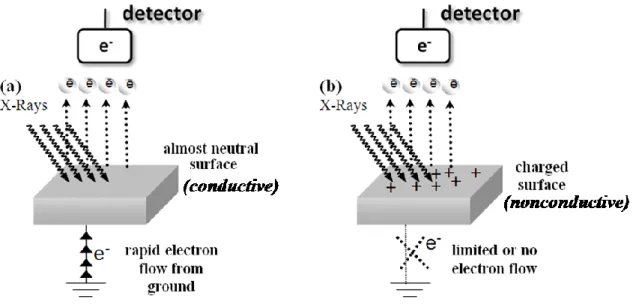
During XPS measurement, an electron current flows from the sample to the electron energy analyzer as illustrated in Figure 4. As a consequence of this, the emission of photoelectrons from the sample may cause a positive uncompensated charge accumulation, which is referred as “surface charging” in the literature.20-22
Actually this event also causes a binding energy variation in the XPS spectrum, if the sample is not grounded or a poorly conductive one as modeled in Figure 4. A number of methods have been developed for charge compensation.23, 24 However, previously published works by different groups including ours, confirm that if the surface charging is properly utilized, it can be a valuable tool for obtaining extra information about the surface electrical and chemical structure of the sample in the nanometer scale and at the molecular level.22, 25-42 This technique is named as the “controlled surface charging”.6
In general, the measured binding energy, i.e. the peak position, may vary due to the presence of internal and external factors such as creation of photoelectrons, size43 and morphology,44, 45 orientation46, 47 of specimens and the surrounding electrostatic conditions of the examined atoms. These factors can be considered as internal parameters. External parameters include; applying voltage stress, exposing to stray, and low-energy electrons, ions, photons, chemical spices, etc.22, 28, 30-33, 35, 38-42, 48-51 These intentional and unintentional variations in peak position (or the binding energy shifts) have been tried to be controlled or compensated by employing a variety of techniques. A completely neutralized experimental condition during XPS analysis is only an ideality because the charging process is a dynamical one and is usually governed by more than one parameter, and/or might be influenced by more than one time domains.
10
Figure 4. Charging processes in (a) a conductive and (b) a nonconductive material during
recording of XPS data.
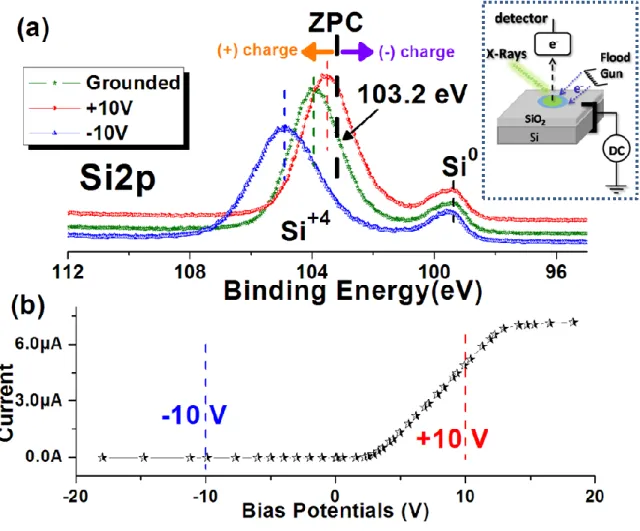
Applying an external bias potential is one way to vary the positions of photoelectron peaks. For this purposes, a DC stress can be employed to create a potential contrast between different dielectric domains of a sample. In addition, the operation of the flood gun during XPS measurements provides focused low energy electrons on the sample with a specific spot size, intensity, and kinetic energy as illustrated in the inset of Figure 5. For demonstration of this effect, a Si wafer which has a thermally grown oxide layer of a ca. 8 nm will be used. The Si2p region of the SiO2/p-Si sample is recorded while the sample
is grounded, and while it is also subjected to negative and positive 10 V bias potentials. When a -10 V DC bias is applied to the sample, the corresponding peak shifts to a lower binding energy because the applied potential also affects the kinetic energy of emitted photoelectrons. If the sample is a nonconductive one, an additional small shift appears toward the higher binding energy due to a positive charge accumulation on the sample. For the positive DC potentials an opposite situation takes place, since the low energy
11
electrons are pulled by the sample, to create negative charge accumulation on the sample. The repelling and pulling of the low energy electrons can also be monitored by measuring the total current passing from the sample under varied DC potentials as demonstrated in Figure 5b. When the negative potentials are employed, the current is limited to a 10-20 nA value due only to the presence of a x-ray induced photocurrent, which is not affected by the applied bias. When the applied bias changes to positive values, the sample attracts low energy electrons, so a larger current starts to pass through the sample around µA levels which increases linearly by the amplitude of the applied DC bias. The biased spectra are corrected as much as the amplitude of the external potential to make better comparison among the three spectra. Under normal conditions, the Si2p peak of the metallic Si (Si0) appears at 99.5 eV, and that of the silica domains (Si+4) at 103.2 eV which correspond the zero-point-charge (ZPC) states.25, 52 As shown in Figure 5a, the Si2p peak of the pure Si is not affected from the applied bias, once the correction is carried out. This means that the pure silicon has enough-conductivity for our measurements. However, the peak of the silica domains is shifted in opposite directions and is broadened due to accumulation of inhomogeneous charges at different conditions. To determine the amount of charging on the silica domain, the value of corresponding peak position must be compared with the value of the ZPC. A measured peak position higher than the ZPC means that a positive charge is accumulated, and a negative charge accumulation causes a shift to lower values. As shown in Figure 5a, the sample at all three different conditions has positive charges, but the magnitude of the positive charge is different. At -10 V DC bias, it accumulates a larger amount of positive charge compared with the grounded and at +10V. Therefore, the DC biased XPS technique is a simple way
12
to determine the presence of surface charging. For example, using with this method one enhances the dissimilarities of different dielectric domains.6, 25, 42
Figure 5. (a) XPS spectra of the Si2p region of a SiO2/p-Si sample connected to ground
(green) and to +10 V(red) and – 10 V (blue) external DC stresses. The thickness of the silica overlayer is ca. 4 nm. (b)The variation of the current passing through the sample under various bias potentials. The inset on the top right depicts the experimental setup.
Similar experiements can also be carried out using a squarewave electric excitation for probing the controlled surface charging in a time-dependent or dynamic fashion. To illustrate the methodology, a Au metal strip is chosen as the sample, and an externally introduced resistor and capacitor pair to impart a dielectric type of a behavior to it.6 As
13
Au is one of the best conductive materials, the binding energy positions of photoelectron peaks are equally altered by application of the squarewave stress in the absence of resistor-capacitor pair. This result can be monitored by XPS as represented in Figure 6a,b. Grounded Au metal has an Au4f5/2 spin-orbit doublet peak at 84.00 eV and the
squarewave electric stress twins the peaks because the sample is subjected to a positive potential during one half of the SQW cycle and to a negative potential during the other half. Therefore, peak separation between the twinned Au4f peaks is always 20.00 eV as demonstrated in Figure 6b. Measurement of exactly a 20.00 eV binding energy difference (B.E. Diff.) translates to the absence of any charge accumulation and/or dissipation. The B.E. Diff. only deviates from a value of 20.00 eV when an external resistance exists in addition to the system: (Au+R). Hence, a less than 20.00 eV B.E. Diff. of the Au+R system is measured at any frequency, with no time dependence as illustrated in Figure 6c. The time dependence is observed only after incorporation of a capacitor to the system: (Au+RC). Therefore, the Au+RC system has a less than 20.00 eV B.E. Diff. at low frequencies while the half duration of the squarewave stress is long enough for ensuring a fully or partially charged and/or discharged state. But, the deviation from 20.00 eV B.E. Diff. recovers at high frequencies because the sample does not have enough time to charge and/or discharge as depicted in Figure 6d. Therefore, by applying external electrical stress and controlling the flow of the low energy electrons, the charge on the sample can be controlled and electric parameters similar to resistance and capacitance values can be extracted from a set of dynamic XPS measurement at different frequencies.35, 38-42
14
Figure 6. XPS spectra of the Au4f region, when the metal is connected externally to; (a)
ground; (b) SQW excitation of ±10.00 amplitude and at frequencies of 10 kHz (navy spectrum) and 0.001 Hz (magenta spectrum). The same spectra are reproduced after connecting to an external circuit, consisting of; (c) a series resistor (R=220 kΩ); (d) a series resistor and a parallel capacitor (R=220 kΩ, C=500 nF). A schematic diagram of the experimental set-up is given as an inset, where IX-ray represents the electron current
due to photo and secondary electrons generated, and IFlood is the current due to the
flood-gun used.
1.2. Photoconductivity
Photoconductivity is an optically induced electrical phenomenon for some of the semiconductive materials, which can basically be described as a conductivity enhancement or resistivity reduction of the semiconductor under photoillumination with an appropriate energy.53 When adequate numbers of photons are absorbed by the
15
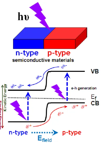
material, electrons are excited from their valance band to their conduction band and/or from mid-gap states such as trap, defect, surface, acceptor, and/or donor related ones, existing between the conduction and the valance band. This process creates an electron-hole pair in the semiconductor. If this event occurs in between or near a junction of n- and p- doped semiconductors, the generated electron and hole pairs are favorably separated from each other. This phenomenon is called charge separation as shown in Figure 7. The charge separation is an important topic and numerous works on this subject convey us that it has crucial potential in applications involving solar cells as a renewable energy source. In addition, the future projections about the energy production techniques indicate that it is one of the most promising technology to meet energy demand of the entire world in the near future.54 Fortunately today’s semiconductor technology assures us that generated electron-hole pairs can be separated from each other by applying proper potentials or well-designed devices with better band gap engineering.55
The conductivity of a semiconductor is defined as,53
σ = neµ (4) where n is the density of charge carrier, e is the elementary charge constant (1.602 x 10⁻¹⁹ Coulombs), and µ is the mobility of charge carrier at a certain temperature. Furthermore, from definition of photoconductivity any variation in conductivity can be expressed a summation of individual changes of independent variable as follows,53
16
Figure 7. Photoinduced electron-hole generation and separation in between n- and p-type
semiconductor.
For our experimental setup, the number of charge carriers can only be affected by introducing a light source or changing its intensity level in certain ways. However, an increase in the intensity level of the light source causes also an increment in the level of the density of charge carriers if the recombination rate of electron-hole pairs is slower than its generation rate. When this condition is fulfilled, we can assume that there is a correlation between the intensity of the light and the variation in the density of charge carriers in the absorbed region of the semiconductor. The mobility of charge carriers is another important parameter for the conductivity of semiconductive materials, and it can
17
safely be assumed to be constant for our measurement system because the temperature of analyzed sample is around room temperature, and a few degree variation in the temperature of the sample under both laser and x-ray irradiations is not expected to create a significant electrical conductivity change.55, 56
1.3. Surface Photovoltage
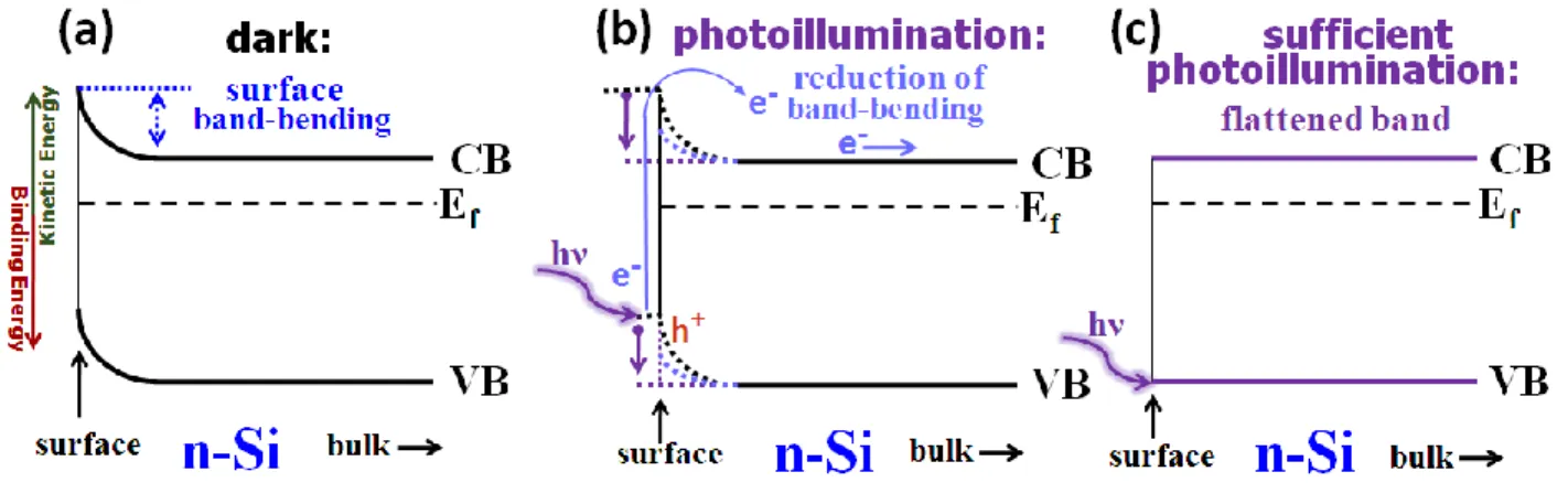
Surface photovoltage is a surface related phenomenon for semiconductive materials and occurs due to presence of band-bending phenomenon at the surface of the semiconductor.57-60 The band-bending on semiconductive materials has both intrinsic and extrinsic factors. While doping type and amount, dangling bonds, and surface defects/states can be considered as intrinsic factors, the deliberately or unintentionally absorbed surface species and external stresses such as temperature, electric and magnetic field, etc. are possible extrinsic factors.58, 61 Under the effect of these factors the surface states of a semiconductor converges to an energy value which promotes a certain amount of charge rearrangement between its surface and bulk. For example, an additional electron accumulation at the surface of n-Si gives rise to an upward band-bending in dark conditions as illustrated in Figure 8a. Under photoillumination, electrons are excited from the valance band to the conduction band. This process might cause a reduction in the extent of the band-bending or even a flattened band condition in the presence of under a sufficient photoillumination as demonstrated in Figure 8b and 8c, respectively. In contrary, a downward band-bending is present for p-Si, which will be elaborately in detail in the following passages
18
Figure 8. The band diagram of n-Si (a) in dark (b) under photoillumination and (c) in
flattened conditions. Adapted from the references 57, 58, 59, and 60.
The surface photovoltage phenomenon becomes a more intensely concerned subject day by day as a result of inventible size shrinkage of electronic device, so previously negligible surface-related effects become more dominant at smaller scales. Measurement of surface photovoltage involves determining both magnitude and type of polarization of trapped charges or built-in potentials at the surface under light illumination. Usually the surface photovoltage corrects the accumulation of charges due to the band-bending by diminishing the built-in electric field. Kelvin Probe (KP) has been the commonly employed technique to evaluate surface photovoltage so far due to its simplicity.58, 61-63 However, the KP technique does not have any chemical specificity, and it is not more than a well designed surface-compatible electrometer. Previously reported works show that XPS is another technique to directly monitor surface photovoltage with a certain reliability and chemical sensitivity.57, 59, 64-70 Moreover, the modern XPS instruments have the ability to record the data in the snapshot mode, which provides a fast data acquisition with ca. 0.1 second time resolution for a narrow energy range from a few eV upto 40-50 eV energy window. While this speed of data acquisition is far away from the time domains of fast process involving electron excitation and electron-hole recombination
19
with the time constants of pico to nano seconds,66, 67, 69-76 nonetheless, a sub-second time resolved spectroscopy still allows probing dynamics involving dipole and polarization type processes.51, 77 For example, the time constants of some of the charge accumulation and dissipation processes in dielectric and insulator type layersare around or just below a time scale of second. Hence such process can easily be monitored with the fast data acquisition method of XPS.42, 49-51, 78
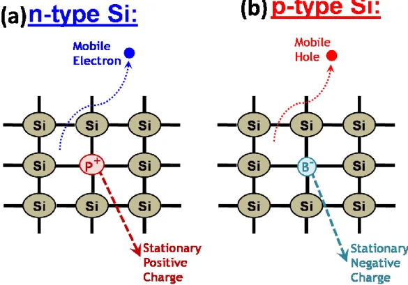
As discussed before the distinct surface electronic structure of semiconductors causes upward and downward band-bending for the n-type and p-type doped semiconductors, respectively.57-59, 67 As it is well established, the different chemical properties of dopant atoms cause drastic changes on electrical properties of semiconductor. For example, if we assume that there is no surface related effect(s) on a Si wafer; namely no band-bending, then a n-type phosphorus, P doping into Si crystal introduces a stationary positive charge on itself and a mobile negative charge into semiconductor as illustrated in Figure 9a. For p-type boron, B doped Si, the stationary charges are negative and they are trapped onto dopant B atoms while the mobile positive charges are delocalized into the system as illustrated in Figure 9b.55, 56 The upward band-bending of an n-type semiconductor is the result of the built-in electric field at the edge or surface of semiconductor due to mainly the discontinuity of the lattice, namely surface effect. This electric field is damped by pushing of the mobile negative charges to the surface of n-type semiconductor and remaining stationary positive charges onto dopant atoms inside the bulk of the solid. Meanwhile, the entire system has still a totally zero charge. However, the charges are different and vary from the surface to the bulk, which causes a depletion region (bended
20
band). The average length of the depletion region for Si was reported to be around 100 nm range as illustrated in Figure 8,10.67
Figure 9. The representative Si lattice structures of the n- and p-type doped with (a) P (b)
B elements. Adapted from the references 55 and 56.
Owing to the 10 nm depth sensitivity of the XPS technique, the charge accumulation at the surface of n- and p-type semiconductors can be measured by XPS. The band-bending of n-type semiconductor causes a certain amount of energy shift, which can be reduced by exposure to sufficiently energetic and intense photoillumination, which is also called surface band-flattening58, 62 as measured and modeled in Figure 10a,b. As a result, the flattening of the upward band-bending of the n-type Si is monitored at a higher binding energy of the Si2p peak under photoillumination. Similarly, the downward band-bending of the p-type Si exhibits an opposite shift, and is called p-type surface
21
photovoltage shift as shown in the right panel of Figure 10. In other words, the surface band-bending effects of the n- and p- type doped Si might be reduced or entirely removed by proper photoillumination as they are measured by XPS to be +0.11 and -0.19 eV shifts, respectively. Unfortunately, the commercially available lab-based XPS instrument has an elemental sensitivity about ~0.1 atomic percent, and, it does not have sufficient sensitivity to probe directly the dopant atoms. However, the dopant dependent photoelectron peak shift can be traceable with XPS due to referencing or correcting of the peak position with respect to the pinned Fermi levels.
Figure 10. (a) The XPS spectra and (b) band diagram of n- and p-type doped Si without
and with exciting light source (violet laser). While the left panel belongs to n-type Si, the right panel belongs to p-type Si. The dotted green circular and line indicates effect of light source onto both band diagram and XPS spectra of n- and p- type doped Si.79
(a)
(b)
22
2. Aim of Work
The electrical and optical properties of today’s high-end technologic devices such as photovoltaics, photonics, optoelectronics, sensors, etc, become more crucial due to the required dramatic reduction in the size of such devices to reach faster processing powers with lower energy consumption. Moreover, the thickness of the semiconductor layer in such devices has already been downsized to few tens of atomic layers, so that the properties of the interfaces between different types of junctions and/or materials have become more pronounced. In this project we deal with a similar complexity for trying to distinguish voltage variations due to charging, surface photovoltage, and photoinduced conductivity changes developed in the semiconductive layers and/or at interface between different semiconductive layers as well as their substrates in a chemically addressed fashion.
SiOXNY/Si,37, 80 SAMs/SiOX/Si,52, 81, 82 polymer and/or metallic
nanoparticles/SiOX/Si,28, 38, 39, 83, 84 HfOX/Hf,85-87 AlYOX/Al and WOX/W,30 GeOX/Ge,88
and SiOX/Si,28, 31, 34, 35, 78, 88-92 systems have been extensively investigated by Suzer’s
group for better understanding the nature and the mechanism of charging/discharging properties which are vital for developing next generation devices. For that, a technique has been developed for recording the shifts in the positions of the XPS peaks in response to different forms of electrical stimuli for probing dynamics of charging/discharging processes of thin dielectric films, which we have named as “Dynamic XPS”. Modulation of the electrical signals in the form of square waves at different frequencies enables us to extract certain dielectric properties such as effective resistance and capacitance values in a chemically resolved fashion. This makes XPS a more powerful technique for
23
characterizing today’s demanded nano or optoelectronic devices. Besides, these early published results have shown us the power of XPS as a charge sensitive technique.
In the present work, we have introduced photoillumination as an additional form of the external stimulus and investigated the combined optical and electrical responses of different semiconductive material such as n- and p-type Si samples and with thermally grown ca. 5 nm silica overlayer, as well as n- and p-type GaN, and CdS films samples which were grown using different routes. The present contribution is a continuation of our earlier work, where we try to distinguish between electric and photo-induced processes. Furthermore, these findings allow us to demonstrate that XPS is a surface characterization technique to track the potential variation on the sample under photoillumination. All these methodologies allow us to extend the Equation 1 and add new terms to extract potentials created by optical and electrical stimuli both in static and dynamic fashions, expresses as;
BE= hυ – KE ± eV ± eQ/C ± eI∆Rph ± eSPV (6) where V, Q, C, I, Rph, SPV, and e are bias potential, accumulated charge, capacitance,
current, photoresistance, surface photovoltage, and elemental electron charge, respectively. The use of this equation will be elaborated in the “results and discussion” part.
24
3. Experimental
3.1. Sample Preparation
The Si wafers (100) were purchased from the institute of electronic materials technology via the “www.universitywafer.com”. Phosphor and boron doped n- and p-type Si wafers are one side polished wafers, and the values of resistivity are reported as 10-20 Ω·cm and 28-31 Ω·cm, respectively. The wafers are washed with acetone or ethanol to remove surface contaminants and dried under nitrogen flow. Then the wafers are left in a concentrated HF solution for 2 min to remove the native oxide layer on the substrate and other chemically bonded organic/inorganic contaminants. Afterwards, the wafers are washed again firstly with de-ionized water and subsequently with acetone to remove any unwanted species. Finally, they are dried under nitrogen flow one more time. This procedure provides a bare Si sample without much of a native oxide layer up to 30 min in atmosphere at room temperature.
The surface patterned Si wafers were manufactured with a high power fiber coupled near-infrared laser by the group of Dr. Ömer İlday (Physics Department of Bilkent University).93-95 The doted, 2D scanned, and line shape patterned substrates were prepared for investigating with XPS. In addition, several patterned Si substrates were chemically cleaned with HF before the process to discriminate any laser induced chemical modifications by avoiding residual oxides. The usual laser patterning process was performed in atmosphere.
25
The CdS film was grown on the Si substrate by laser ablation technique and obtained from the group of Dr. Attila Aydınlı (Physics Department of Bilkent University). The successive ion layer absorption and reaction (SILAR) technique96 was also performed to achieve ultra thin high quality CdS layers on Si substrate containing ca. 5 nm thermally grown oxide layer. Initially the Si substrate was treated with 0.01 M NaOH for further cleaning and obtaining chemically more active surface to increase homogeneity of the films. Subsequently, the substrate was immersed into sequentially Cd2+ cation (0.05M) and S2- anion (0.05M) solutions successively to grow thin CdS films. A washing step of substrate with de-ionized water was followed after each ion bath step.96 The ionic and washer solutions were frequently replaced with fresh solutions. The thickness of films can be controlled by increasing the number of immersion cycle, and we did not perform any annealing step.
A commercially available CdS based photoresistor (OEM) was used to probe a location depended resistance investigation. The encapsulated polymeric overlayer of the photoresistor for moisture-resistance, optical focusing and antireflection features were lifted off with acetone. An ultrasonic shaker treatment with acetone solution is employed for a further cleaning step during a 30 second period. After lifting off and washing processes, the photoresistor immediately was transferred into the ultra-high vacuum chamber to prevent oxidation and/or contamination. The virgin sample was analyzed without further ion etching, except for performing chemical depth profiling experiments.
The GaN samples were grown on double polished c-plane sapphire with a low-pressure metalorganic chemical vapor deposition (MOCVD) system (AIX 200/4 RF-S) in the group of Dr. Ekmel Özbay (Physics Department of Bilkent University). The Si doped
26
n-GaN had a thickness of 1 µm with ~ 1.2x10+13 cm-3 electron carrier concentration and ~300 cm2/V.s mobility. The Mg doped p-GaN was ~0.5 µm thick with hole concentration of 4.5x10+17 cm-3 along with a mobility of 11 cm2/V.s.
GaN is a wide band gap semiconductor and the band gap is reported as a direct one97 and its value is reported as 3.4 eV.98 For our photoillumination measurements we have employed four different lasers; violet (405 nm), green (532 nm), red (635 nm) and near-infrared laser (980 nm) the corresponding photon energies are 3.1, 2.3, 2.0, and 1.3 eV, respectively. Therefore, even with the violet laser, excitation is not band to band, but a sub-band excitation. The sub-band excitation has advantages and disadvantages which will be discussed in the “results and discussion” section.
CdS and GaN samples were etched with the Ar+ ion gun of the XPS instrument employed to get rid of surface carbon and oxygen contaminants as much as possible till we reached a point that it was below the detection limit of our XPS instrument. Although, the kinetic energy of Ar+ ions can be accelerated upto 4 kV, usually a low energy value (1-3 eV) has been chosen to avoid surface damage. This is a crucial point because even a small amount of damage can completely change electronic properties of semiconductors, so extreme care must be exercised during usage of the ion gun. For example, while Ar+ ion etching of the CdS sample with a 3 kV kinetic energy for about one hour duration does not leads to Ar atom implantation into CdS sample, on the other hand significant amount of damage and insertion of Ar+ ions could easily be incorporated into the Si wafers. For example, when Si wafers cleaned with Ar+ even for a short time and a low kinetic energy power (such as a ten second exposure duration with 200 V kinetic energy),
27
the Ar peaks started to be detected with XPS. Therefore, for most of our measurements reported in this thesis Si based samples were not cleaned with ion gun.
3.2. Instruments and Technique
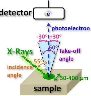
All of the XPS measurements were carried out using a ThermoFisher K-Alpha XPS instrument which is furnished with a monochromatic Al Kα (at 1486.68 eV) x-ray source. The operational chamber pressure is usually kept around 10-9 mbar. The X-ray beam is directed to the sample with a 550 incidence angle with respect to sample normal via a quartz crystal which also provides monochromatic filtration of the x-rays as demonstrated in Figure 11. The electron energy analyzer is located at the top of the sample with a 900 orientation with respect to the surface plane of sample. Hence the take-off angle is 900. An electrostatic lens system is employed to collect photoelectrons from a ±300 solid angle from the normal. The electrostatic lenses also collimate and re-focus the emitted photoelectron to the entry slit of the hemispherical electron energy analyzer, so the actual take-off angle from the sample surface is a 600 solid angle as illustrated in Figure 11. As a standard stability checking experiment of x-ray flux of the instrument with an Ag reference sample, the instrument yields >3 million counts per second at 200 eV pass-energy from Ag3d5/2 line which also has one of highest x-ray absorption cross section.
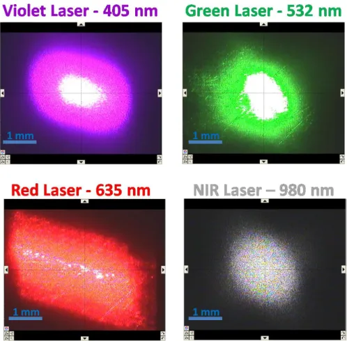
The spot size of the x-ray beam can be chosen from 30 to 400 µm diameter, but a 400 µm spot size is used for most of our measurements, unless otherwise mentioned. Three electronic CCD cameras (Bosch LTC0455/11) are mounted on the chamber of the K-Alpha system to assist sample transportation and to ensure superimposed intersection of the sample for x-ray, ion and flood guns with a better than 1 µm precision.
28
Figure 11. The arrangement of experimental setup of the K-Alpha instrument.
The instrument has a resistive array detector with 128 individual channels. In a normal scan mode, all energy channels of detector are used for averaging output to improve signal to noise ratio, so the required experiment time significantly decreases for a reasonable resolved spectrum in this mode. The detector also provides an energy resolution that is better than 0.02 eV.
In the snapshot mode, the detector can make parallel counting for different energy windows and allows recording a narrow range spectrum at only one dwell time of ca. 0.1 s. We recognized that this duration was not consistent with real experimental measurement time. After an efficient collaboration between the Surface Analysis Department of the ThermoFisher Co. and our team, this lag-time is now reduced to 50-70 ms by avoiding assigning of same settings for successive snapshot measurements. Now the fastest data acquisition speed between successive snapshots is shorter than 0.1 s with reasonable energy resolution and signal to noise ratio. This speed is important for us
29
because some charging/discharging processes have time constants in this time scale. Therefore, these types of processes can now be traced for the first time with a lab based XPS instrument, although, the synchrotron type sources and special multi-channeltron based detectors can have been reported to record data much faster than our speed (0.1 s) due to both higher brightness of the light sources and dedicated detector systems.70, 74
Several other modifications were also made on the standard sample holder of the K-Alpha system to achieve an electric connection port. Now, the sample holder can be externally connected either to the ground, a DC power supply, or to a pulse generator from both top and bottom sides of the sample as illustrated in Figure 12. Our electrically isolated sample holder can also provide an extra ground connection on the sample, so devices can now be analyzed during a more realistic electrical operation conditions by driving a sufficient amount of current to extract electrically resolved and chemically addressed data with just one probe. Stanford Research System DS340 is used as the pulse generator for our dynamic XPS measurement. In addition, Stanford Research System DS345 is used to generate sweep frequency of the squarewave function to gather faster impedance type measurements.
The K-alpha spectrometer is equipped with a flood and an ion gun unit. The ion gun can be operated to generate energetic Ar+ beams at kinetic energies between 200 V and 4 kV to clean the sample and/or to obtain depth profiles. The flood gun is used to neutralize sample’s surface during the measurements. The flood gun generates fluxes of low-energy electrons and Ar+ ions at 0-2 eV and around 20 eV kinetic energies, respectively. The kinetic energy of low energy electron and Ar+ ion fluxes can also be controlled.