PLASMONICALLY ENHANCED SILICON
INFRARED SCHOTTKY DETECTOR
A THESIS
SUBMITTED TO THE DEPARTMENT OF ELECTRICAL AND ELECTRONICS ENGINEERING
AND THE GRADUATE SCHOOL OF ENGINEERING AND SCIENCES OF BILKENT UNIVERSITY
IN PARTIAL FULLFILMENT OF THE REQUIREMENTS FOR THE DEGREE OF
MASTER OF SCIENCE
By
Kazım Gürkan Polat
September 2011
ii
I certify that I have read this thesis and that in my opinion it is fully adequate, in scope and in quality, as a thesis for the degree of Master of Science.
Assist. Prof. Dr. Ali Kemal Okyay (Supervisor)
I certify that I have read this thesis and that in my opinion it is fully adequate, in scope and in quality, as a thesis for the degree of Master of Science.
Assoc. Prof. Dr. Vakur B. Ertürk
I certify that I have read this thesis and that in my opinion it is fully adequate, in scope and in quality, as a thesis for the degree of Master of Science.
Assist. Prof. Dr. Gökhan Özgür
Approved for the Graduate School of Engineering and Sciences:
Prof. Dr. Levent Onural
iii
ABSTRACT
PLASMONICALLY ENHANCED SILICON INFRARED
SCHOTTKY DETECTOR
Kazım Gürkan Polat
M.S. in Electrical and Electronics Engineering
Supervisor: Assist. Prof. Dr. Ali Kemal Okyay
September 2011
The holy grail of near infrared (NIR) photonics is a purely-Silicon-based solution. Today, infrared detection is dominated by III-V compound semiconductors, mainly InGaAs devices in the NIR. The high cost of integration with established Si VLSI technology, prevent the market growth of compound semiconductor device technology despite high efficiencies attained. On the other hand, Silicon is the second most abundant element on the earth and is the predominant material of the complementary metal-oxide-semiconductor (CMOS) technology. Since Silicon is near infrared blind due to its large energy bandgap (~1.12 eV) it cannot absorb infrared light efficiently. However, Silicon based Schottky photodetectors can operate at infrared wavelengths due to their absorption mechanism at the interface of metal and semiconductor. The metal-semiconductor (M-S) diode is among the most investigated junction devices. Schottky diodes have been very attractive for their high speeds. The potential of high frequency operation and the ease of integration render Schottky devices a strong candidate in CMOS compatible NIR photonics. Silicon based Schottky photodetectors can be a promising candidate if NIR efficiencies could be increased. We design, fabricate and characterize plasmonic gratings to increase the efficiency of Silicon based Schottky photodetectors at the near infrared region. Our design is optimized for the conventional telecommunication C-band
iv
(1530 nm-1650 nm). We also study the effects of an interlayer dielectric and metal layer on the plasmonic fields. We use atomic layer deposited Alumina (Al2O3) between the metal and the semiconductor at the M-S junction. Our
micro/nano-fabricated photodetector devices exhibit low dark current densities (~21 mA/cm2 at -3 V) and high responsivity values (~83 mA/W at 1530 nm and -3V). Plasmonic gratings provide an increase of responsivity by more than a factor of 2 at desired wavelengths.
Keywords: Schottky, photodetector, near infrared detection, plasmonics,
v
ÖZET
PLAZMONİK YAPILARLA GELİŞTİRİLMİŞ SİLİKON
KIZILÖTESİ SCHOTTKY ALGILAYICI
Kazım Gürkan Polat
Elektrik ve Elektronik Mühendisliği Bölümü Yüksek Lisans Tez Yöneticisi: Yrd. Doç. Dr. Ali Kemal Okyay
Eylül 2011
Yakın kızılötesi fotonik teknolojilerinin geleceği tamamen Silikon tabanlı çözümlerle olacaktır. Günümüzde, III-V grubu bileşikler ve özellikle de InGaAs tabanlı algılayıcılar yakın kızılötesi algılamada en çok kullanılan, en gelişmiş aygıtlardır. Yüksek verimliliklerine rağmen oturmuş Si CMOS teknolojisiyle tümleşiminin pahalı olması, bileşik yarıiletken aygıt teknolojilerinin pazar gelişimini engellemektedir. Diğer taraftan, Silikon doğada en çok bulunan ikinci elementtir ve Bütünleyici Metal-Oksit-Yarıiletken (CMOS) teknolojilerinin ana malzemesini oluşturmaktadır. Si tabanlı optoelektronik aygıtlar yüksek (~1.12 eV) yasak bant enerjileri nedeniyle yakın kızılötesi dalgaboylarında kördür ve kızılötesi ışığı verimli bir şekilde emememektedir. Fakat, Silikon tabanlı Schottky fotoalgılayıcılar metal ve yarıiletken arayüzündeki emme mekanizması sayesinde kızılötesi dalgaboylarında çalışabilmektedir. Metal-yarıiletken diyotlar en çok araştırılmış bağlantı aygıtlarındandır. Schottky diyotlar yüksek hızları sebebiyle çok ilgi görmüştür. Potansiyel yüksek frekans uygulamaları ve kolay tümleşim özellikleri Schottky aygıtları CMOS uyumlu yakın kızılötesi fotonik için güçlü bir aday yapmaktadır. Eğer yakın kızılötesi verimlilikleri arttırılabilirse. Silikon tabanlı Schottky fotoalgılayıcılar bud alga boyları için umut vaad eden bir aday olabilirler. Biz bu çalışmada Silikon tabanlı Schottky fotoalgılayıcılarının yakın kızılötesi dalgaboylarındaki verimliliklerini arttırma
vi
adına plazmonik ızgara dizaynı, üretimi ve karakterizasyonu yaptık. Dizaynlarımız konvansiyonel telekomünikasyon C bandı (1530 nm- 1650 nm) için optimize edildi. Ayrıca tabakalar arası dielektrik tabakasının ve metal tabakasının plazmonik alanlara etkileri çalışıldı. Atomik düzeyde kaplamayla Alumina (Al2O3) metal ve yarıiletken arasına kaplandı. Mikro ve nano
ölçeklerde üretilen fotoalgılayıcı aygıtlar düşük karanlık akım ( ~21 mA/cm2 ve -3 V) ve yüksek duyarlılık (~83 mA/W, 1560 nm ve -3V) değerleri gösterdiler. Plazmonik ızgaralar amaçlanan dalgaboylarında iki kattan fazla duyarlılık artışı sağladılar.
Anahtar Kelimeler: Schottky, fotoalgılayıcı, yakın kızılötesi algılama,
vii
Acknowledgements
I owe my profound gratitude to my supervisor Dr. Ali Kemal Okyay for his never ending and friendly guidance throughout my thesis studies. He made productive suggestions without any hesitation and motivated me during my thesis.
I would like to thank specially Dr. Vakur Ertürk for being in my thesis committee and sharing his useful comments. I would also thank personally to Dr. Gökhan Özgür and Melikşah University for their support. I am also indebted Dr. Necmi Bıyıklı and Dr. Bülend Ortaç for their useful comments regarding my fabrication and characterization processes.
I would also thank my all Okyay team members, former Demir group members and UNAM colleagues who have contributed my research including Levent (simulations), Fatih (wire bonding), Efe (setup interface), Adem, Ahmet, Alper, Cagla, Cahit, Engin, Feyza, Inci, Koray, Oguz, Temmuz …
I am very proud to dedicate my thesis to my father; Nazmi, my mother; Necla, my sisters; Gokcen and Goknur, my brother-in-laws; Engin and Yakup and especially my little niece Yagmur. I show my appreciation to my sister Gokcen and my brother-in-love Engin for their endless support during my studies.
viii
Lastly, I offer my regards to Ozgur, Onur and Akin for their support in any respect.
ix
Table of Contents
Abstract ... iii Özet ... v Acknowledgements ... vii Contents ... ix List of Figures ... xi 1 INTRODUCTION ... 1 1.1 Problem Statement ... 1 1.2 Motivation ... 2 1.3 Objectives ... 31.4 Organization of the Thesis ... 4
2 DEVICE PHYSICS ... 5
2.1 Plasmonics Overview ... 5
2.1.1 Surface Plasmons ... 8
2.1.2 Localized Surface Plasmons...10
2.1.3 FDTD (Finite-Difference Time-Domain) method...11
2.2 Photodetector Overview ... 12
2.2.1 Schottky-Barrier Photodetector... 13
3 DEVICE FABRICATION ... 17
3.1 Substrate and Surface Preparation ... 17
3.2 Dielectric Film Coating ... 19
3.3 Photolithography and Development ... 19
3.4 Etching... 23
3.5 Interlayer Dielectric Coating... 23
3.6 Metallization and Lift-off ... 24
x
4 CHARACTERIZATION ... 28
4.1 Simulation Results... 28
4.2 Current-Voltage Measurements ... 35
4.3 Responsivity Measurements... 37
4.3.1 Optical Measurement Setups ... 37
4.3.2 Plasmonic Enhancement of Responsivities ... 40
4.3.3 Interlayer Dielectric Thickness Study ... 44
4.3.4 Adhesion Metal Thickness Study ... 45
5 CONCLUSIONS AND FUTURE DIRECTIONS ... 47
xi
List of Figures
Figure 2.1 Lycurgus Cup a) under daylight illumination and b) under
illumination from inside (this image is under courtesy of British Museum) ... 6
Figure 2.2 Count of the articles containing “surface plasmon” in the title from 1980 to 2010 ... 7
Figure 2.3 Coordinate system for metal / dielectric interface ... 8
Figure 2.4 Schematic representation of surface plasmons in the TM mode ... 9
Figure 2.5 Absorption of photons (a) first detection mode: band-to-band excitation (b) second detection mode: internal photoemission ... 13
Figure 2.6 Energy band diagram of a Schottky photodetector ... 14
Figure 2.7 Quantum efficiency as a function of photon energy ... 16
Figure 3.1 Photographs of cleaved Silicon wafers with diamond pen ...18
Figure 3.2 a) Multilevel CAD design of Schottky photodetectors, b) Optical microscope image of metallization lift-off mask, c) closer view of one device at the mask ... 20
Figure 3.3 Lift-off procedure both for direct and image reversal photolithography ... 22
Figure 3.4 Mask design of FIB patterns ... 25
Figure 3.5 a) SEM image of completed Plasmonic Schottky device, b) close up SEM image showing grating structures ... 26
Figure 3.6 a) SEM image of devices with two different FIB mask ...27
Figure 4.1 a) Schematic representation of Schottky photodetectors and (b) Gold grating design on Si with parameters p: period, t: thickness, w: width and also polarization of incidence light ... 29
Figure 4.2 a) Structure of the one period using Lumerical interface, b) override mesh regions, c) same structure in b) with mesh grids Figure 4.3 Electric field intensity is integrated over interface and normalized with respect to periodicity is given for arbitrary unit for constant thickness 250nm, width 1150nm ... 30
xii
Figure 4.4 Electric field intensity is integrated over interface and normalized
with respect to periodicity is given for arbitrary unit for constant period 1250nm,
thickness 250nm ... 31
Figure 4.5 Electric field intensity is integrated over interface and normalized with respect to periodicity is given for arbitrary unit for constant period 1250 nm, width 1150 nm ... 32
Figure 4.6 Electric field intensity profile inside gold grating for constant period 1250 nm, width 1150 nm. X-axis is for metal width and Y-axis is for metal thickness... 33
Figure 4.7 Absorbed power graph vs. wavelength for different Alumina thicknesses... 33
Figure 4.8 Absorption of gold layer with an increase of Titanium layer for different wavelengths ... 34
Figure 4.9 I-V curve of the device under no illumination and (inset) SEM image of the device ... 35
Figure 4.10 dark and illuminated (microscope lamp) I-V curves ... 36
Figure 4.11 a) Schematic representation b-c) photographs of the setup ...38
Figure 4.12 a) Schematic representation b) photograph of the setup ... 39
Figure 4.13 Responsivity of fabricated photodetectors with a period 1250 nm, metal width 1150 nm and thickness 250 nm. ... 40
Figure 4.14 Photodetectors with different metal width. Distance is equal to period minus width. Period is 1250 nm and thickness is 250 nm. Light is p-polarized ...41
Figure 4.15 Responsivity of fabricated detector at p-polarized light ...42
Figure 4.16 Responsivities at different wavelengths for large photodetectors at -5V bias ... 43
Figure 4.17 Responsivity for Alumina thickness variation ... 46
1
Chapter 1
Introduction
This thesis describes our recent developments and contributions to Silicon based optoelectronic device technology in terms of design, fabrication and characterization of novel Schottky photodetectors. In this chapter, overview of the problem, our motivation and outline of this thesis is given.
1.1 Problem Statement
Today, near infrared detection has a very crucial role in telecommunication and detection applications such as night surveillance systems, infrared cameras. These growing technologies dramatically increased the demand to the materials used in these systems. State of the art near infrared detection technology is based on group III-V compounds and especially InGaAs technology [1][2]. Since the detectors based on these materials offer high functionality and increased performance, they found an interest despite other drawbacks. High tunability of the direct band energy [3] and low dark currents by lattice matched materials [4] made them very favorable in the market. However, high material cost is an important issue that needs to be taken into account. There is an ongoing argument whether Indium reserves are sufficient or not for the future.
2
This leads researches to search for new materials for the market. Also integration difficulties with Silicon based CMOS technology prevent market growth.
Photodetectors operating at the infrared wavelengths are the crucial elements for telecommunication, measurement and night surveillance systems. Since there is an enormous market, low cost materials are needed with competitive efficiencies. Silicon is the second most abundant material on the earth after oxygen, however Silicon is near infrared blind due to its large indirect bandgap (~1.12 eV) and direct bandgap (~3.4 eV). Silicon based Schottky photodetectors can operate at infrared wavelengths due to their absorption mechanism at the interface of metal and semiconductor. Silicon based Schottky photodetectors can be a promising candidate if NIR efficiencies could be increased.
1.2 Motivation
Schottky photodetectors have been intensively investigated due to their high speeds and low contact resistances in the telecommunication and measurement systems in the 0.8μm to 1.65μm wavelength range. Since the overall speed of a cascaded system is highly dependent on the slowest element, it is important to choose every element properly. Also low contact resistance means low delays, which is critical from a systems perspective.
Metal-semiconductor based device design is among the oldest system in semiconductor devices. This well developed system has a vital property. Fabrication needs only one type of dopant and a metal. There is no need for epitaxial growth, implantation techniques or multi quantum well designs. This makes relatively very simple fabrication processes, thus low cost operational procedures.
3
Silicon is the second most abundant material on the earth after Oxygen. As a result of this, Silicon is very cheap and there is no risk for reserves. On the other hand, one of its counterparts Indium is very rare and there is a debate on estimation of its supply years [5]. Also Silicon based Schottky detectors are fully integrated with complementary metal-oxide-semiconductor (CMOS) technology. CMOS is the current state of the art technology for electrical circuits and InGaAs based optical devices have difficulties with the integration progress.
Although Silicon is infrared blind, due to internal photoemission process present in Schottky photodetectors, they can generate photocurrent from photons with lower energies than the bandgap of Silicon. This process allows near infrared light detection using Silicon with lower efficiencies than band-to-band absorption. At this point, we propose an enhancement method to increase efficiency of Silicon based Schottky detectors for near infrared detection. In this thesis, metallic gratings optimized for enhanced absorption of Silicon based Schottky photodetectors at near infrared wavelengths.
1.3 Objectives
Plasmonics is a very hot topic and finds interest from wide range of application areas [6]. Current near infrared detection technologies are highly dependent on Germanium and III-V compounds mainly InGaAs based optical device technologies.
This thesis mainly focuses on the development of alternative Silicon based Schottky photodetectors with an implementation of plasmonic structures in order to increase the efficiency at desired wavelengths and combine the other excellent features of Schottky devices. Design, fabrication, characterization and analysis of these photodetectors are presented in this thesis.
4
1.4 Organization of the thesis
In this part, a brief outline of the thesis is given. Chapter 2 presents a review of plasmonics and device principles of photodetectors mainly focused on Schottky-barrier photodetectors. Chapter 3 gives a detailed explanation of Silicon based Schottky photodetectors. Chapter 4 discusses the characterizations of the fabricated photodetectors and obtained results. Chapter 5 ends the thesis with a conclusion and gives suggestions for the future work.
5
Chapter 2
Device Physics
In this chapter, a short history of plasmonics will be explained and surface plasmons and localized surface plasmons will be discussed. A brief description of finite difference time domain simulations will be given. Secondly, there is a brief overview of photodetectors. Lastly, important performance parameters of photodetectors will be described.
2.1 Plasmonics Overview
As a subfield of nanophotonics, plasmonics mainly focuses on electromagnetic fields in the order of or even smaller than the wavelength. This consequence of light and metal interaction is described by the surface plasmon theory [7][8][9][10].
Interestingly, Romans knew nanoparticle fabrication. They fabricate silver and gold nanoparticles and used them for coloring glasses. First known application of surface plasmons is the Lycurgus Cup (4th century A.D.), which is now in British museum. This cup represents King Lycurgus of Thrace being dragged into the underworld. The color of this cup changes from green to red
6
when illuminated from inside. Under daylight, it shows green color, however nanoparticle excitation occurs while illuminating from inside. Figure 2.1 shows the Lycurgus Cup and its color change due to inside illumination. This cup and also stain glass windows from the 10th, 11th and 12th centuries has metallic nanoparticles that affect the color.
Figure 2.1 Lycurgus Cup a) under daylight illumination and b) under illumination from inside [11] (this image is under courtesy of British Museum)
Maxwell Garnett was the author of the first published article that examines the effect of metal-doped glass to create different colors [12]. He used Drude method and Rayleigh’s derivations for small spheres. Few years later, Gustav Mie made the widely used theory on light scattering by spherical particles [13]. This theory led to the further understanding of surface plasmons.
Since 1950’s research on plasmonics gain importance and receive great boosts along the way. Ritchie [14], Kretschmann [15] and Otto [16] made significant contributions to the area and sparked an interest in other researchers. Also another major increase to the field arrived when new nanoscale fabrication technologies and simulation tools are created in the mid 1990’s. These
7
technologies enabled previously unobtainable results to control surface plasmon properties.
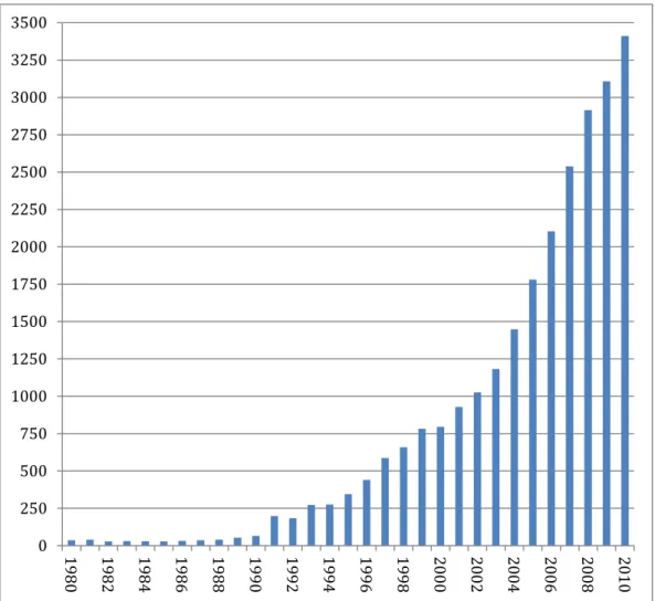
Fig. 2.2 shows the number of published articles containing “surface plasmon” in the title for each year from 1980 to 2010. Although this not the exact number of papers in this field for each year, it gives an important clue about the growth of the field.
Figure 2.2 Count of the articles containing “surface plasmon” in the title from 1980 to 2010 [17] 0 250 500 750 1000 1250 1500 1750 2000 2250 2500 2750 3000 3250 3500 1980 1982 1984 1986 1988 1990 1992 1994 1996 1998 2000 2002 2004 2006 2008 2010
8
2.1.1 Surface Plasmons
Surface plasmons are coherent electromagnetic waves that are present at the interface of two materials where the real part of dielectric constant changes sign between the two materials (e.g. metal-dielectric interface). Usually this is observed in metals such as Au, Ag and Al. Incident photons excite metal dielectric interface and enable free charges in the metal to make oscillations. In 1998, Thomas Ebbesen was the first researcher who showed an extraordinary light transmission through subwavelength holes and made use of nanoscale fabrication techniques. Fabrication of nanoscale features make possible to control the properties of surface plasmons and found an interest from different areas.
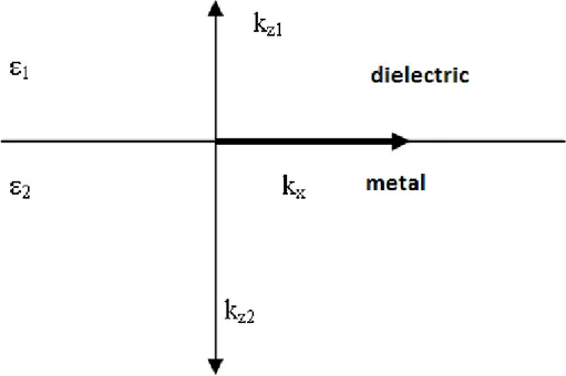
In order to understand the conditions that formed surface plasmons we start with a metal/dielectric surface and coordinate system in Figure 2.3. Although we deal with metallic structures with nanometer scale, Maxwell’s equations hold and we can describe using these equations.
9
Since the electric field propagating in an electromagnetic wave can be described as:
(2.1)
Using appropriate boundary conditions and continuity relation for the TM (Transverse Magnetic) mode (p-polarization), this equation can be solved as [18][19]:
(2.2) and
(2.3)
(2.4)
If we solve these equations, dispersion relation for a propagating wave on the surface between dielectric and the metal becomes:
(2.5)
This condition (2.2) only satisfied when the two materials have opposite signs of the real parts of the dielectric permittivity, in our case metal and dielectric. Figure 2.4 represents the surface plasmons for the TM mode. For the TE (Transverse Electric) mode (s-polarization) this boundary conditions and continuity relation leads to the case where no surface plasmons can exist.
10
Figure 2.4 Schematic representation of surface plasmons in the TM mode [20]
Since the dielectric constant for metals are both complex and negative, surface plasmon mode always has a greater momentum (kx) than free space
photon momentum (k0= w/c) of the same frequency . This situation causes a
momentum mismatch, which prevents free space light coupling directly to the surface plasmon mode. To overcome this mismatch problem, there are three main concepts in the literature. One solution where periodic gratings in the metal layer are used is the main idea in this thesis to design and implement plasmonic resonators for Schottky photodetectors.
2.1.2 Localized Surface Plasmons
We know that surface plasmons are the electromagnetic waves that are propagating between the metal and the dielectric surface. Localized surface plasmons are non-propagating resonances that occur due to excitation of metal electrons with the incident electromagnetic wave. Localized surface plasmons can be seen both inside of the metal and in the near fields. In contrast to the surface plasmons, localized surface plasmons can be excited under TE and TM mode [21]. Localized surface plasmons are observed due to sharp surface edges and necessary penetration depth.
11
Localized surface plasmon based absorption enhancement is observed in various optoelectronic device architectures where the absorption enhancement is maintained via metallic gratings placed at illuminated layer. If localized surface plasmon resonances occur in the absorbing layer, the absorptivity of the active material increases.
2.1.3 FDTD (Finite-Difference Time-Domain) method
The FDTD (Finite-Difference Time-Domain) method is one of the primary computational electrodynamics approaches that solve Maxwell’s curl equations in time domain. Since it is a time domain method, FDTD solutions can cover wide range of frequencies in a single simulation. Since it is a time domain solver and generally FDTD simulators are used for electromagnetic fields as a function of wavelength, it is required to take its Fourier transform during the simulation. FDTD method discretizes the curl equations and uses grid based modeling methods.
The basics of this algorithm are first introduced by Kane Yee in IEEE transactions on Antennas and Propagation in 1966 [22]. Finite-difference time-domain and its acronym “FDTD” terms are coined by Allen Taflove in IEEE Transactions on Electromagnetic Compatibility in 1980 [23]. At present, FDTD modeling is used in a wide range of applications like photonic crystals, nanophotonics, biosensors, microwaves and so on [24]. The simulations used in this thesis are performed using commercial FDTD software developed by Lumerical Solutions Inc. Vancouver, Canada [25].
Lumerical software is a CAD tool in which structures can be formed and material types can be generated using complex refractive indices with respect their frequencies. These features enable to operate with experimentally measured complex dielectric constant of materials. First step of a simulation is
12
to generate structures and assign material types. Secondly build simulation region, select the source type and place the data monitors in this region.
2.2 Photodetector Overview
In its simplest form, a photodetector consists of a p-n junction that generates mobile carriers due to absorption of photons in a semiconductor. An incident photon with a greater energy than the energy bandgap of the semiconductor makes an excitation of an electron from valence band with leaving a hole to conduction band. Bandgap energy that has same energy carried by the photon at a wavelength is given as:
(2.6) Where Eg is bandgap energy, h is Planck constant, c is velocity of light in
vacuum and is corresponding wavelength.
Absorption of photon generates an electron-hole pair in the semiconductor. If this electron-hole pair can be collected by an applied or build-in electric field, this is called photocurrent. This absorption process can be done through direct bandgap or indirect bandgap of a semiconductor. In indirect semiconductors (e.g. Si and Ge) photon absorption process is required a momentum change usually by a phonon.
There are various photodetector types such as Schottky, p-i-n, Avalanche, metal-semiconductor-metal (MSM). Since thesis is mainly focused on Schottky barrier photodetectors, this overview is continued with Schottky photodetector characteristics.
13
2.1.1 Schottky-Barrier Photodetector
The Schottky-barrier photodetector is also called a metal-semiconductor photodetector. This photodetector type has an additional detection mode than other types of photodetector. First detection mode is operated through an electron-hole generation from band-to-band (energy-gap) excitation in the semiconductor. This mode is the common absorption method for all photodetectors. Second detection mode is operated through emission of carriers from metal to the semiconductor over the Schottky barrier. The second detection mode is also referred as internal photoemission. These two modes of photon absorption are illustrated in Figure 2.5.
Figure 2.5 Absorption of photons (a) first detection mode: band-to-band excitation (b) second detection mode: internal photoemission [26]
In applications requiring visible wavelength detection to achieve higher barrier height, it is common to use n-type semiconductor. The semiconductor layer is usually p-type where it requires small barrier height for long wavelength detection [27].
14
Figure 2.6 Energy band diagram of a Schottky photodetector [28]
In Figure 2.6, energy diagram of Schottky photodetector is depicted. As the electrons-hole pair generation occurs, electron concentration in the semiconductor region near the boundary changes. This region is called as depletion region and the length of this region is given by [29]:
(2.7) where, Nd is the ionized donor density, ε is the dielectric constant of the
semiconductor, Vbi is the built-in potential, V is the applied voltage.
There are four different mechanisms for carrier transport in Schottky-barrier photodetectors: (1) carrier generation (or recombination) in the depletion region, (2) thermionic emission, (3) tunneling through barrier, (4) carrier generation (or recombination) in the neutral region of the semiconductor. The large field separates carriers generated in the depletion region rapidly and the internal quantum efficiency if near 100% [30]. Outside of the depletion region these photo-generated carriers can only be collected by diffusion, thus reduces the internal quantum efficiency:
15
(2.8)
where is the optical absorption coefficient and Lp is the minority carrier
diffusion length. This leads overall internal quantum efficiency to:
(2.9)
(2.10)
For internal photoemission, the photon is absorbed in the metal layer and an electron is excited to a higher energy level. These hot electrons have momentum in random directions. Only the hot electrons, which have excess energy than the barrier height and the momentum directed to the semiconductor can contribute to the photocurrent. Unlike the energy-gap excitation process, the internal photoemission is highly energy dependent, and the quantum efficiency is:
(2.11) where C1 is the Fowler emission coefficient and qb is the barrier height. When
a photodetector is illuminated with different wavelengths the quantum efficiency has a threshold of qb and it increases due to an increase in photon energy.
However, after the energy reaches to the band-gap energy, the quantum energy increases highly and it is relatively less energy dependent. Figure 2.7 shows the quantum efficiency change as a function of energy.
16
Figure 2.7 Quantum efficiency as a function of photon energy [31]
Responsivity is an important parameter for understanding the optical to electrical conversion efficiency. Responsivity is the generated photocurrent due to subjected optical power. It is a similar metric with quantum efficiency and here is the relationship:
(2.12)
17
Chapter 3
Device Fabrication
All of the fabrication processes are conducted in UNAM laboratories, class 100 and class 1000 facilities at UCF (UNAM Cleanroom Facilities) and ARL (Advanced Research Laboratories) at Bilkent University. This chapter provides a detailed explanation of the process steps for the fabrication of Schottky photodetectors.
3.1 Substrate and Surface Preparation
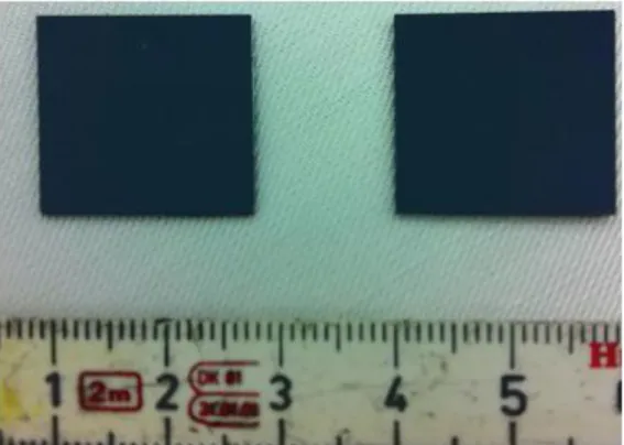
4 inch Silicon lowly doped p-type wafers are used for the Schottky photodetectors. These wafers are cleaved into 23mm x 23mm small pieces and fabrication is performed on these small pieces. 21mm x 21mm mask size is used for this fabrication. Although yield is reduced, this enabled to have multiple samples from 4” wafer. Since the orientation of the Silicon wafers are (100), it was easy to cleave it with the traditional technique. Backside of the wafers is scratched with a diamond tipped scriber and samples with desired dimensions are prepared. Another way to cleave the wafers is using dicer machines. However, it is not preferred in this fabrication in order to prevent the surface
18
from Silicon nanoparticles. In Figure 3.1, images of cleaved Silicon wafers can be found.
Figure 3.1 Photographs of cleaved Silicon wafers with diamond pinned scriber pen
It is very crucial to clean the surface at the beginning and after each fabrication steps. Since we start the fabrication with Silicon wafers, it is ideal to start with standard RCA (Radio Corporation of America) cleanings. Initially, large residues are cleaned with acetone ((CH3)2CO), isopropyl alcohol
((CH3)2CHOH) and methanol (CH3OH). Each step is performed by dipping a
q-tip into the solvent and cleaning the surface with it. Then, 10 minutes of Piranha (H2SO4: H2O2 (4:1)) mixture is prepared for the first step of the cleaning. After
that, samples are treated in (1:50) HF: H2O mixture for a few seconds to remove
oxide on the surface since piranha solution is oxidizing. After this step samples are exposed to H2O:HCl:H2O2 (5:1:1) solution for 10 minutes in order to remove
trace metals. After continuing with HF:H2O step for a few seconds, cleaning of
19
(DI) water and dried by nitrogen gun. A dehydration step is performed in order to remove water on the surface. To check the cleanliness of the sample, an optical microscope is used.
3.2 Dielectric Film Coating
Dielectric film is used for electrical surface passivation for pads. This layer is extremely important for photodetector fabrication since it reduces the dark current leaked thorough pads. Typically contact pads in our devices are 100 times greater in than device active areas. This makes isolation very crucial in order to have low dark current levels. Quality of the dielectric film is also very essential since full isolation is needed from contact pads.
In our Schottky photodetector fabrication, Silicon dioxide (SiO2) is used as
passivation layer for contact pads. SiO2 is coated using Plasma Enhanced
Chemical Vapor Deposition (PECVD) system VAKSIS CVD-Handy in UCF. Conformal deposition of SiO2 films are realized by optimizing gas flow rates,
chamber temperature and RF power. Process gases are N2O (200 sccm) and
SiH4 (200 sccm). RF power is 10W and temperature is 250oC at 0.45 mT
pressure. 120 nm of SiO2 is coated in 6 minutes and this thickness is verified
using J. A. Woolam V-VASE Ellipsometer at UNAM and stylus profilometer KLA Tencor P6 surface profiler in UCF.
3.3 Photolithograph and Development
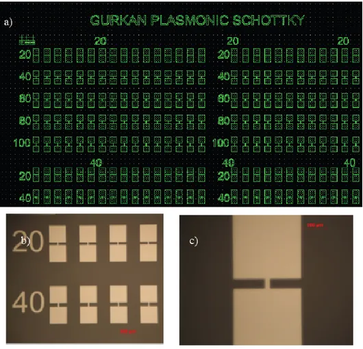
Photolithography process is the method to transfer patterns onto the surface. A photo mask is designed and implemented using Layout Editor (GNU GPL) tool [32]. The mask writing is performed with a Heidelberg Instruments DWL-66 Mask Writer in UCF. We designed a two-mask process to fabricate samples that
20
are ready for Focused Ion Beam (FIB) procedure. First mask layer is to pattern Silicon dioxide used as isolation pads and the second mask is used for patterning metal layer. In Figure 3.2, mask patterns and design of the mask using CAD software can be found.
Figure 3.2 a) Multilevel CAD design of Schottky photodetectors, b) Optical microscope image of metallization lift-off mask, c) closer view of one device at the mask
Sample surface is coated with photoresist – a UV sensitive polymer – using Laurell WS650SZ-6NPP-lite spinner. Photolithography enables to define the regions to be coated or etched on each fabrication step.
It is very crucial to start the photolithograph with the same surface conditions on every sample. For this reason surface cleaning and surface dehydration is
a)
21
very critical to have repeatable results. To remove the humidity on the surface, we bake the samples at 110oC for 3 minutes using a hot plate. For small sized features, adhesion promoters are used to have better resolutions. Hexametyldisilazane (HMDS) layer can be used as an adhesion promoter. Since we can achieve the features repeatedly, we usually skip this step. We use AZ5214E type of AZ Electronics Materials photoresist (PR) in our fabrications. This photoresist can be used both positive and negative tone. We use the photoresist with 4000 rpm for 40 seconds spinning parameters and resulting resist thickness of 1.4 m. After coating the photoresist there is a pre-bake step for 55 seconds at 110oC using hot plate. This step removes the solvents in the photoresist and prevents sample stick to the mask during alignment. Electronic Vision Group EVG620 Mask Aligner is used for alignment and UV exposure with constant dose (~75 mJ) at first photolithography step.
In first photolithography step we use direct photolithography since we aim to etch Silicon dioxide from patterned regions. After UV exposure, the parts of the photoresist, which are subjected to the UV light, become soluble in the developer. We use AZ400K developer at every photolithography step as developer. Develop solution (AZ400K:H2O = 1:4) is prepared and samples
developed for approximately 40 seconds in this solution. However, it is very important to observe the samples during development step. During the etching away of the soluble photoresist, one can detect the color change on the samples and decide to optimal timing for development. To finalize the development, samples are immediately rinsed in DI water in order to remove developer on the substrate. A post-bake step is performed after development at 120oC for one minute using hot plate. This step utilizes features with better resolution.
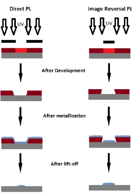
In the second photolithography step, image reversal photolithography is used in order to get better results from lift-off process. Sidewalls of the photoresist after development step are different between direct photolithography and image reversal photolithography. Figure 3.3 shows lift-off process for image reversal
22
and direct photolithography visually. Angle of the sidewalls at direct lithography is not suitable for metal lift-off process in our fabrication so we applied image reversal photolithography to our samples. In image reversal lithography, there are additional steps before development to the direct lithography. After the first exposure (~75 mJ), samples are baked at 120oC for 2 minutes and exposed to the UV light without using the mask at a dose of 200mJ. After these steps development procedure and post bake is performed to complete image reversal lithography.
23
3.4 Etching
After completing photolithography, etching process is done in order to pattern the desired features to the layers under the photoresist. There are two methods for etching. Wet etching is done by preparing necessary solutions and dipping samples. Secondly, dry etching makes use of ions and plasma for the etching process.
Due to our design choices, we use dry etching since scum formation is an important effect, which sometimes occurs during wet etching. Dry etching is done using STS LPX SR Inductively Coupled Plasma (ICP) in UCF. Photoresist is used as mask, CHF3 (100 sccm) O2 (20 sccm) is used for SiO2 etching. 13.56
MHz coil power is 250W and platen at 380 KHz is 30W. Process pressure is 50 mT and the temperature is 20oC. Etch rates acquired using dummy samples and same duration is applied for photodetector samples. Etch profiles are inspected using Stylus profilometer and optical microscope to ensure all SiO2 is etched.
3.5 Interlayer Dielectric Coating
Interlayer dielectric film is especially important to understand the Schottky barrier effects and plasmonic behaviors of fabricated photodetectors. To be able to realize this, extremely high quality dielectric films required. These films can deposit using Atomic Layer Deposition (ALD) equipments. Conformal deposition of dielectric between metal and semiconductor layers is crucial in order to isolate metal and semiconductor. Al2O3 is deposited using Cambridge
Nanotech ALD Savannah in UCF. Al2O3 is grown using DI water and
Trimethylaluminum (TMA) precursor. Process temperature is 250oC and flow rate is 20 sccm. Growth is done with 0.015 second pulse intervals. Growth cycles counts are planned depending on the necessary thickness. Each cycle
24
deposits a layer of approximately 0.106 nm of Alumina. It is very critical to clean the surface prior to the deposition. Since the RCA cleaning procedures does not affect important layers for fabrication, we use the same cleaning steps as substrate preparation step. HF dipping etches SiO2, however thickness of this
film is not crucial unless it isolates the pads.
3.6 Metallization and Lift-off
After completing dielectric film coating using ALD, a photolithography step is performed in order to pattern the areas where metal will remain on the sample. This step is done with image reversal photolithograph techniques to acquire enhanced lift-off results. Schottky contacts are formed using metal evaporation.
Different Au thicknesses and adhesion metal choices of Ti are studied in this research. During interlayer dielectric thickness study, ultra thin (~3nm) Ti layer is used as adhesion layer for Au (250nm). Throughout adhesion metal effect study, Ti with different thicknesses are used as adhesion metal and 250nm of gold used. VAKSIS Thermal Evaporator is operated for Ti deposition. Gold is coated using the same equipment as the adhesion metal. Samples are rotated during evaporation for uniform coating. After metallization is finished, samples are left in acetone in order to remove excess metal. Lift-off process can take several hours to complete. If necessary, additional sonification can be done for complete removal of excess metal.
25
3.7 FIB Etching
Optimized design of plasmonic gratings for the target wavelength region, cannot be achieved using standard photolithography techniques. Our simulation results gave best performances when the grating period is 1.25 m with a 100 nm distance between metal fingers. The smallest feature that can be achieved using optical lithography is ~1m range. Since it is not possible to resolve 100 nm features with optical lithography, we design a mask using Layout Editor (GNU GPL) tool with our desired gratings. FEI Company Nova 650i Nanolab Focused Ion Beam (FIB) at UNAM is used to etch the designed features. Beam current, dwell time, overlap optimization is done in order to obtain best results. Figures below show schematic representation, SEM images of completed photodetectors and close up images of the FIB patterns.
26
Figure 3.5 a) SEM image of completed Plasmonic Schottky device, b) close up SEM image showing grating structures
a)
27
Figure 3.5 a) SEM image of completed devices with two different FIB mask
a)
28
Chapter 4
Characterization
This chapter gives information on obtained simulation results and describes the optoelectronic device characterization of the fabricated devices and discusses the achieved results. Device characterization involves electrical and optical characterization of the fabricated photodetectors and includes optical micrograph and SEM measurements of these devices.
4.1 Simulation Results
In order to enhance the device performance at near infrared wavelengths, first we design our structures optimized especially for the conventional C-band (1530-1565 nm) telecommunication wavelength range. We conducted our simulations using a commercial FDTD simulation package by Lumerical Inc.
The effect of interlayer Alumina (Al2O3) dielectric is investigated
numerically. Another study is done using Ti layer as an adhesion metal to the structure. Since Au has adhesion issues when it is coated on Silicon, use of an adhesion metal is common practice for coating of Au. The effect of this adhesion layer thickness is studied to examine the effects of this layer.
29
Figure 4.1 a) Schematic representation of Schottky photodetectors and (b) Gold grating design on Si with parameters p: period, t: thickness, w: width and also polarization of incidence light
Figure 4.1 illustrates important parameters for our simulations. We simulate our design for different gold thicknesses; change the width and the period of the metallic gratings in order to find an optimized structure. Also we define a parameter distance, which is the distance between two metal gratings.
For Finite-Difference-Time-Domain simulations we use Lumerical Inc.’s FDTD Solver with a general aim to determine trends and a guide for our experimental studies rather than a tool to obtain results. We chose this simulation tool since it is widely accepted in nanophotonics. There are more than 200 scientific publications in literature that used this tool [33]. In terms of meshing, auto non-uniform conformal meshing technology provided by Lumerical is used [34]. With this method without losing accuracy of our results, simulation time is reduced. In order to increase accuracy of our simulation results, override mesh regions used at interfaces. The maximum allowed override mesh size was 0.2nm in the direction of interface. Moreover, in the whole simulation region (except inside air which is far from interface) maximum allowed mesh size was 5nm. These mesh size choices are done after careful simulations of much smaller mesh sizes. We observed that further decrease in mesh sizes does not make changes larger than %10 but increases simulation time significantly. Also these small changes do not alter the general trends observed. Moreover, in this point it might be beneficial to remember that the key role of these simulations is to give an idea for absorptivity trend of
30
Schottky metal. Thus, instead of trying to obtain exact numbers of absorption or electric field intensity peaks, we tried to reveal trends of absorptions peaks with respect to our design parameters. Figure 4.2 shows the structure of one period and the mesh regions.
Figure 4.2 a) Structure of the one period using Lumerical interface, b) Override mesh regions, c) Same structure in b) with mesh grids
The performance results of the gold gratings on top of the Silicon layer is defined as the absorption enhancement at gold layer close to semiconductor interface in 5nm range. The designs are illuminated from the front side with a spectral range 1500nm to 1600nm. TEM polarized source which has electric field perpendicular to gratings as shown in Figure 4.1 b is used. In our simulations, we calculated total electric field intensity at the metal layer close to the semiconductor. We assumed that absorbed photons inside Schottky metal generates hot electrons and if they are sufficiently close to semiconductor they can pass Schottky barrier. With a cautious assumption, we choose 5nm as the distance that these hot electrons can move on Schottky barrier. Also to have a fair comparison, calculated total electric field intensity is normalized with period of gratings. After this point, “light intensity” will be used instead of normalized
31
total electric field intensity close to semiconductor. Figure 4.3 shows the light intensity results with respect to period and wavelength for constant metal thickness (250 nm) and metal width (1150 nm).
Figure 4.3 Electric field intensity is integrated over interface and normalized with respect to periodicity is given for arbitrary unit for constant thickness 250nm, width 1150nm.
As it can be seen from the Figure 4.3 there is a strong electric field intensity peaks with a recurrence ~45 nm of wavelength change due to an increase of ~50 nm in period. The best light intensity is ~5 and present at 1250 nm period at 1550nm wavelength and the corresponding gold thickness is 250 nm and metal width is 1150nm. If we look at the light intensity variation for wavelengths due to width change at constant period and thickness we observe that light intensity does not change due to slight variations in distance. Figure 4.4 illustrates these variations.
32
Figure 4.4 Electric field intensity is integrated over interface and normalized with respect to periodicity is given for arbitrary unit for constant period 1250nm, thickness 250nm
When we look at the light intensity factor variation due to the thickness change with respect to wavelength for a constant period and width we find out that thickness changes affect light intensity significantly. Figure 4.5 represents these variations for a constant period of 1250nm and width 1150 nm.
We conclude from these simulation results that to have a light intensity peak at the conventional C-band (1530 nm-1565nm) telecommunication wavelengths, we aimed to fabricate with parameters period (1250 nm), thickness (250nm) and width (1150nm).
33
Figure 4.5 Electric field intensity is integrated over interface and normalized with respect to periodicity is given for arbitrary unit for constant period 1250 nm, width 1150 nm
In order to understand the effects of hot electrons, we study the effects interlayer dielectric to the device performance. First we look at the position of the generated plasmon profile in the metal and find out that electric field intensity drastically increases at the interface and the metal edges when there is no interlayer dielectric (Figure 4.6). Than we combine these results with interlayer dielectric thickness simulations and adhesion metal thickness simulations.
34
Figure 4.6 Electric field intensity profile inside gold grating for constant period 1250 nm, width 1150 nm. X-axis is for metal width and Y-axis is for metal thickness
Figure 4.7 Absorbed power vs. wavelength for different Alumina thicknesses.
35
After simulating our structures with different Alumina thicknesses between the metal and the semiconductor, we observed that absorbed power peak shifts due to an increase in the Alumina layer. Maximum absorbed power increases up to 5 nm of Alumina thickness and decreases after this level. These simulations are done for 1350 nm period, 1250 nm metal width and 250nm of gold thickness. Figure 4.7 shows the achieved results for Alumina thickness study.
The adhesion metal (Titanium) thickness results show that increasing the Ti thickness does not shifts the peaks very much, however it dramatically decreases the absorption of gold layer. Figure 4.8 illustrates the observed results of Titanium thickness variation for 1350 nm period, 1250 nm metal width and 250nm of gold thickness. These simulations also have an Alumina layer of 3 nm at the interface of the semiconductor and metal.
Figure 4.8 Absorption of gold layer with an increase of Titanium layer for different wavelengths
4.2 Current-Voltage Measurements
Device characterization of the fabricated Si based Schottky photodetectors begins with current-voltage (I-V) measurements. Dark current measurements are
36
performed under no illumination and inside of the Faraday cage using Keitley 4200 SCS Semiconductor parameter analyzer in UNAM Clean Room (UCF) and Cascade Microtech PM-5 probe station in UCF. Illuminated I-V characteristics are measured using microscope illumination (visible light) of the probe station to observe the I-V curve shift due to photocurrent generation under illumination.
Figure 4.9 shows the dark current measurement of a fabricated device with no Alumina layer and 3nm Titanium as an adhesion layer. This device has a period of 1350 nm, metal width of 1250 nm and gold thickness of 250 nm.
Figure 4.9 I-V curve of the device under no illumination and (inset) SEM image of the device
Fabricated devices are operated under reverse bias for photodetection mode operation and leakage voltages are very low. We illuminate the samples
37
under microscope illumination in order to observe the rectification of the current at reverse bias. It was not possible for this setup to understand photocurrent since we don’t have a control of wavelength and lock-in amplifier. Figure 4.10 shows the rectification of the I-V curve under illumination. To have a better observation current scale is changed to logarithmic. These devices show low dark current densities (21 mA/ cm2) and comparable with the literature.
Figure 4.10 dark and illuminated (microscope lamp) I-V curves
Dark current levels of all devices including interlayer dielectric thickness study and the adhesion metal thickness study showed similar results. Since the effect of these studies can be clearly viewed during photocurrent measurements we continue with the responsivity measurements.
38
4.3 Responsivity Measurements
Responsivity and quantum efficiency measurements are performed to reveal optical detection and the plasmonic enhancement profiles of the fabricated Silicon based Schottky detectors. Xenon light source with a monochromator and 1510 nm-1620 nm (tunable wavelength) coherent fiber coupled laser sources are used to demonstrate the generated photocurrent behaviors.
4.3.1 Optical Measurement Setups
First responsivity setup is used with Oriel Apex illuminator with Xenon light source and monochromator. Light output at the end of the monochromator is passed through a 2-lens system in order to reduce the beam spot size. Incident light is aligned to the device with a micrometer driven xyz stage. However, fabricated photodetectors have a size of 20 m to 20 m and the beam spot is much larger than this. This prevents actual responsivity measurements. All responsivity measurements made with this setup are arbitrary due to this situation. Light beam is chopped with a frequency of ~1300 Hz and photocurrent data are obtained using Stanford Research Systems SR830 lock-in amplifier. Optical power is measured with a calibrated InGaAs photodetector and used in responsivity calculation. Commercial InGaAs detector used in this measurement have dimensions of 5 mm to 5 mm and as it is mentioned before our devices are 20 m to 20 m. This causes arbitrariness to our measurements. We achieve responsivity values divided by an unknown factor around 50000. Figure 4.11 shows the schematic representation and the photographs of the first measurement setup.
39
Figure 4.11 a) Schematic representation [35] b-c) photographs of the setup
b)
40
Second measurement is used with a 1510 nm-1620 nm (tunable wavelength) laser as a light source. Output of the laser is collimated using a collimator and chopped in order to use lock-in amplifier. After the chopper a microscope objective is used to focus the beam. Also an infrared camera is used with the same objective and gives the opportunity to focus the light directly to the sample. A light beam spot size smaller than 200 m is achieved using this setup. We fabricated a device with 250 m to 250 m dimensions and measure the actual responsivity of it using this setup. Figure 4.12 has the schematic representation and the photographs of the second measurement setup.
41
4.3.2 Plasmonic enhancement of responsivities
In order to observe the responsivity enhancement at desired wavelengths using our plasmonic structures, we design different measurements and fabricate different gratings. Surface plasmons are only observed at TM mode (p-polarization). The output of the light source at first optical setup is non-polarized characteristics, so we introduce a polarization-maintaining cube to achieve polarized light. Then we measure the generated photocurrent for different polarizations and read it from lock-in amplifier. After dividing it with optical power, we acquire the responsivities of these devices. Note that, these are not actual responsivities with Ampere over Watt units. These values have arbitrary units. We applied a voltage bias of -3V to these devices.
Figure 4.13 Responsivity of fabricated photodetectors with a period 1250 nm, metal width 1150 nm and thickness 250 nm.
Maximum absorption enhancement of this device is seen at 1560 nm wavelength at the simulation results. Photocurrent maximum is seen at 1530 nm. This shift can be caused by a thickness variation or the imperfectness during the
42
grating openings at FIB process. Also we simulate our design with built-in material data of the software. Actual values can be a little different and make this variation. These shifts are observed in every measurement. We clearly have an absorption enhancement due to plasmonic gratings. Since surface plasmons are observed only in TM mode (p-polarization), there is no peak in the s-polarization. The non-polarized light is combination of s and p polarized waves, so the enhancement factor reduced due to its s-polarized component.
We fabricate another grating with a simulation result that has a peak at same wavelength and smaller enhancement factor. As it is stated during the simulation part, we slightly change the width of the metallic gratings to decrease the enhancement. The reason of this study is to prove the enhancement is caused by generated surface plasmons. Figure 4.14 shows the responsivity change of the photodetectors.
Figure 4.14 Photodetectors with different metal width. Distance is equal to period minus width. Period is 1250 nm and thickness is 250 nm. Light is p-polarized.
43
Since Silicon starts to absorb light before the wavelengths ~1100nm, we aimed to observe the characteristics of band-to-band excitation and internal photoemission processes. We scrutinize wavelengths from 800 nm to 1650 nm to utilize this experiment. Figure 4.15 represents the responsivity of photodetectors with a metal grating designed for enhancement at 1560 nm wavelength. As it is expected band-to-band excitation is dominated the responsivity for our photodetectors. During this experiment three different filters (yellow, 850 nm and 1100 nm cut-off) are used to suppress the harmonic wavelengths and this may caused the peak at 850 nm and variations at 900 nm-1100 nm wavelength ranges. Since responsivity at smaller wavelengths are too much than longer wavelengths, plasmonic enhancements occur at 1530 nm range is barely observable.
Figure 4.15 Responsivity of fabricated photodetector at p-polarized light
As it is mentioned before, actual responsivity measurements cannot be measured with the first optical setup due to its beam spot size. In order to acquire actual
44
responsivities we did a fabrication with large dimensions (250m x 250m), which is 156.5 times greater than our past fabrications. Second optical measurement setup is used to measure generated photocurrent. Figure 4.16 illustrates the responsivities of these devices. Although this is the actual responsivity values for this device, we expect higher responsivities in our smaller sized devices. During the FIB processes, large sized etch profiles needs higher current levels and this causes shapes with slopes round edges etc. Since we used low current levels in small devices we got features with good resolution. We achieved 83 mA/W responsivity for 1560nm wavelength at -5V bias.
45
4.3.3 Interlayer Dielectric Thickness Study
In order to have a better understanding of plasmonic structures, we planned to add an extra Alumina (Al2O3) layer in between the metal and semiconductor
layer. During our simulations we realized that addition of Alumina layer to the structure shifts the maximum enhancement peak point. Also up to 5 nm thickness of Alumina layer absorption increases and after that thickness it starts to decrease. We fabricated these structures and examine the responsivities. We couldn’t observe that much change at the peak position wavelength but enhancement factors showed similar trends with the simulations. Enhancement factor is higher for the 2 nm case than the sample with no Alumina coated. Enhancement factor is decreased at 5 nm Alumina coated sample; however this is an expected result. Generated hot electrons may be increased for 5 nm case but tunneling of these electrons is not calculated at the simulations. This is also major factor that affects responsivity. Figure 4.17 shows the achieved responsivities with p-polarized incident light.
46
4.3.4 Adhesion Metal Thickness Study
Gold has an adhesion issues with Silicon and it is a common practice to use gold with a metal with better adhesion properties to the Silicon. We used Titanium as an adhesion metal and since it has too little or no plasmonic effects, we aimed to find the effect of Titanium layer to our designs. Simulation results showed that increase in thickness of Titanium drastically decreases the enhancement values. We observe the same trend in our fabricated devices. Figure 4.18 shows the effect of Titanium layer to the responsivity of the devices under p-polarized light.
47
Chapter 5
Conclusions and Future Work
In this study, design, fabrication and characterization of plasmonically enhanced Silicon based Schottky photodetectors are investigated. Performance enhancements at desired wavelengths are demonstrated. Optimized structures for conventional C-band (1530 nm- 1565 nm) telecommunication wavelengths are characterized. Represented photodetectors showed a possible competitive device with low cost and increased efficiencies. Furthermore, Si CMOS technology compatible photodetectors are represented instead of current state of the art In GaAs technology.
In order to improve the device performances and to have more comprehensive study, some future work can be listed. To have better quality simulations of the designed structures, actual n-k data of the materials can be implemented to the software. Also new grating designs may improve the enhancement at near infrared wavelengths. A design that covers a long range of wavelengths can be used in infrared cameras. Different adhesion metals with plasmonic effects such as Aluminum can utilize a better enhancement factors. A few improvements at the optical setup solve the responsivity issues of the measurements. Fiber coupling of the light source with an efficient way can be a
48
solution for this. Different interlayer dielectric materials can be investigated in order to have higher or wider enhancement profiles. A more challenging task, focal plane arrays can be done using these photodetectors.
49
BIBLIOGRAPHY
[1] Website, http://www.thorlabs.com/dsp_CatalogDownload2.cfm?id=47, 2011.
[2] M. Herrscher, M. Grundmann, E. Droge, St. Kollakowski, E. H. Bottcher,
and D. Bimberg “Epitaxial liftoff InGaAs/InP MSM photodetectors on Si,”
Electronics Letters, vol. 31, pp. 1383-1384, 1995.
[3] B. E. A. Saleh, and M. C. Teich, Fundamentals of Photonics, Hoboken, NJ,
USA: John Wiley and Sons Inc., 1991
[4] B. M. Onat, W. Huang, N. Masaun, M. Lange, M. H. Ettenberg, and C.
Dries, “Ultra Low Dark Current InGaAs Technology for Focal Plane Arrays for Low-Light Level Visible-Shortwave Infrared Imaging,” Infrared Technology
and Applications, vol. 6542, pp. 1-9, 2007
[5] "How Long Will it Last?". New Scientist 194 (2605): 38–39. May 26, 2007.
[6] Knight et al., Science, 2011 Vol 332 (6030): 702-704
[7] Barnes, W. L., Dereux, A., Ebbesen, T. W. (2003). “Surface plasmon
subwavelength optics”. Nature, 242, 824-830.
[8] Maier, S. A., Plasmonics: Fundamentals and Applications, Springer (2007)
[9] Brongersma, M. L., Kik P. G., Surface Plasmon Nanophotonics, Springer
Series in Optical Sciences, Springer (2007)
[10] Shalaev V. M., Kawata S., Nanophotonics with Surface Plasmons, Elsevier
(2007) [11]Website, http://www.britishmuseum.org/explore/highlights/highlight_image.aspx?image= k737.jpg&retpage=20945 http://www.britishmuseum.org/explore/highlights/highlight_image.aspx?image= k741.jpg&retpage=20945
[12] J. C. M. Garnett. Colours in metal glasses and in metallic films. Philos.
Trans. R. Soc. London, 203:377, 1908.
[13] G. Mie. Beirtrage zur optik truber medien, speziell kolloidaler
50
[14] R. H. Ritchie. Plasma losses by fast electrons in thin films. Physical
Review, 106:874, 1957
[15] E. Kretschmann and H. Reather. Radiative decay of nonradiative surface
plasmon excited by light. Z. Naturf., 23A:2135, 1968
[16] A. Otto. Excitation of nonradiative surface plasma waves in silver by the
method of frustrated total reflection. Z. Phys., 216:398, 1968.
[17] Webpage, ISI. Surface plasmon publication statistics. http://apps.isiknowledge.com, 2009
[18] Surface Plasmons on Smooth and Rough Surfaces and on Gratings.
Springer Tracts in Modern Physics 111. New York: Springer-Verlag.
[19] Cottam, Michael G. (1989). Introduction to Surface and Superlattice
Excitations. New York: Cambridge University Press.
[20] Website, http://www.amitabh.org/project.html
[21] Maier, S. A., Plasmonics: Fundamentals and Applications, Springer (2007)
[22] Kane Yee (1966). "Numerical solution of initial boundary value problems
involving Maxwell's equations in isotropic media". IEEE Transactions on
Antennas and Propagation 14 (3): 302–307
[23] A. Taflove (1980). "Application of the finite-difference time-domain
method to sinusoidal steady state electromagnetic penetration problems". IEEE
Transactions on Electromagnetic Compatibility 22 (3): 191–202.
[24] Allen Taflove and Susan C. Hagness (2005). Computational
Electrodynamics: The Finite-Difference Time-Domain Method, 3rd ed.
[25] Website, http://www.lumerical.com/
[26] Kwok K. Ng, Complete Guide to Semiconductor Devices, McGraw-Hill
Series in Electrical and Computer Engineering, (1995)
[27] Kwok K. Ng, Complete Guide to Semiconductor Devices, McGraw-Hill
Series in Electrical and Computer Engineering, (1995)
[28] Kwok K. Ng, Complete Guide to Semiconductor Devices, McGraw-Hill
![Figure 2.1 Lycurgus Cup a) under daylight illumination and b) under illumination from inside [11] (this image is under courtesy of British Museum)](https://thumb-eu.123doks.com/thumbv2/9libnet/5951558.124152/18.892.194.764.379.760/figure-lycurgus-daylight-illumination-illumination-courtesy-british-museum.webp)
![Figure 2.4 Schematic representation of surface plasmons in the TM mode [20]](https://thumb-eu.123doks.com/thumbv2/9libnet/5951558.124152/22.892.191.776.187.459/figure-schematic-representation-surface-plasmons-tm-mode.webp)
![Figure 2.5 Absorption of photons (a) first detection mode: band-to-band excitation (b) second detection mode: internal photoemission [26]](https://thumb-eu.123doks.com/thumbv2/9libnet/5951558.124152/25.892.195.741.512.795/figure-absorption-photons-detection-excitation-detection-internal-photoemission.webp)
![Figure 2.7 Quantum efficiency as a function of photon energy [31]](https://thumb-eu.123doks.com/thumbv2/9libnet/5951558.124152/28.892.329.631.193.504/figure-quantum-efficiency-function-photon-energy.webp)