Plasma-Induced Molecular Beam Epitaxy R. Dimitrov, A. Mitchell, L. Wittmer et al.
IOP PUBLISHING SEMICONDUCTOR SCIENCE AND TECHNOLOGY
Semicond. Sci. Technol. 25 (2010) 045024 (7pp) doi:10.1088/0268-1242/25/4/045024
Mobility limiting scattering mechanisms
in nitride-based two-dimensional
heterostructures with the InGaN channel
S Gokden¨
1,6, R Tulek¨
1, A Teke
1, J H Leach
2, Q Fan
2, J Xie
2, U¨ Ozg¨ur¨
2,
H Morkoc¸
2, S B Lisesivdin
3,4and E Ozbay¨
51 Department of Physics, Faculty of Science and Letters, Balıkesir University, C¸agıs¸ Kamp˘ us¨ u,¨
10145 Balıkesir, Turkey
2 Department of Electrical and Computer Engineering, Virginia Commonwealth University, Richmond, VA 23284, USA 3 Nanotechnology Research Center-NANOTAM, Bilkent University, 06800 Ankara, Turkey
4 Department of Physics, Faculty of Science and Arts, Gazi University, Teknikokullar, 06500 Ankara, Turkey 5 Department of Physics, Department of Electrical and Electronics Engineering,
Nanotechnology Research Center-NANOTAM, Bilkent University, 06800 Ankara, Turkey E-mail: [email protected]
Received 24 November 2009, in final form 2 February 2010 Published 16 March 2010
Online at stacks.iop.org/SST/25/045024
Abstract
The scattering mechanisms limiting the carrier mobility in AlInN/AlN/InGaN/GaN two-dimensional electron gas (2DEG) heterostructures were investigated and compared with devices without InGaN channel. Although it is expected that InGaN will lead to relatively higher electron mobilities than GaN, Hall mobilities were measured to be much lower for samples with InGaN channels as compared to GaN. To investigate these observations the major scattering processes including acoustic and optical phonons, ionized impurity, interface roughness, dislocation and alloy disorder were applied to the temperature-dependent mobility data. It was found that scattering due mainly to interface roughness limits the electron mobility at low and intermediate temperatures for samples having InGaN channels. The room temperature electron mobilities which were determined by a combination of both optical phonon and interface roughness scattering were measured between 630 and 910 cm2 (V s)−1 with corresponding sheet carrier densities of 2.3–1.3 × 1013 cm−2. On the other hand, electron mobilities were mainly limited by intrinsic scattering processes such as acoustic and optical phonons over the whole temperature range for Al0.82In0.18N/AlN/GaN and
Al0.3Ga0.7N/AlN/GaN heterostructures where the room temperature electron mobilities were found to be 1630 and 1573 cm2 (V s)−1 with corresponding sheet carrier densities of 1.3 and 1.1 × 1013 cm−2, respectively. By these analyses, it could be concluded that the interfaces of HEMT structures with the InGaN channel layer are not as good as that of a conventional GaN channel where either AlGaN or AlInN barriers are used. It could also be pointed out that as the In content in the AlInN barrier layer increases the interface becomes smoother resulted in higher electron mobility.
1. Introduction
frequency and high-power microwave applications because nitride-based material systems have desirable fundamental Al(In)GaN/(In)GaN-based high electron mobility transistors physical properties, such as a large band gap, large breakdown (HEMTs) have attracted a great deal of attention for high- field and strong spontaneous and piezoelectric polarization 6 Author to whom any correspondence should be addressed. fields [1]. To improve the performance of devices, various 0268-1242/10/045024+07$30.00 © 2010 IOP Publishing Ltd Printed in the UK & the USAbarriers and channel alternatives have been used in nitridebased HEMTs [2–10]. Several achievements have been made by optimizing the growth and design parameters. In recent years, an AlInN barrier layer has been implemented instead of AlGaN to improve the HEMT performance after the original proposal of Kuzm´ık [11]. The advantage of using an AlInN barrier lies in the ability to adjust the composition of the alloys to obtain a lattice- or polarization-matched heterostructure. The HEMTs with nearly lattice-matched AlInN barrier layers were essentially predicted to provide higher carrier densities than in those with an AlGaN barrier layer [12], promising for high-power and high-frequency transistor operations [13].
It has also been reported that the incorporation of an InGaN layer between an AlGaN barrier and a GaN channel in conventional heterostructures leads to a higher carrier density induced by larger polarization fields and its tighter confinement at the interface due to the larger conduction band offset [14]. Lanford et al reported an improvement in the electron transport characteristics by suppressing current collapse with the inclusion of an InGaN channel compared to the conventional AlGaN/GaN heterostructre [15]. However, it is quite difficult to improve the quality of the InGaN channel, so the mobility of two-dimensional electron gas (2DEG) in the InGaN channel is limited to be lower than 800 cm2 (V s)−1 with an ∼2 × 1013 cm−2 sheet carrier density at room temperature [16]. An InGaN layer has also been used as a back barrier in the AlGaN/GaN/InGaN/GaN DH to improve the confinement of the 2DEG and increase the electron mobility in the GaN channel [17–19].
Recently, Xie et al studied the effect of barrier layers on the electron mobility in InGaN channel HEMTs [2]. They reported that with the proper choice of a barrier, such as Al0.24In0.01Ga0.75N, the HEMT containing a 12 nm In0.04Ga0.96N channel exhibited a 1230 cm2 (V s)−1 Hall mobility at room temperature, which is higher than previously reported mobilites in InGaN channels with a conventional AlGaN barrier. Despite these results reported in the literature, there are only a few reports in terms of the detailed analysis of the transport characteristics of HEMTs with the InGaN channel [13, 20, 21].
Inthepresentwork, weinvestigatethetransportproperties of AlInN/AlN/InGaN/GaN heterostructures with different alloy compositions of the AlInN barrier layer in conjunction with conventional AlGaN/AlN/GaN and AlInN/AlN/GaN using temperature-dependent Hall effect measurements. Analytical models were applied to the experimental data in order to understand scattering mechanisms that govern the transport
the scattering mechanisms that are dominant for high-density 2DEGs can be identified, it will guide the optimizaion of the growth and/or the layer structure that will be necessary to further improve the conductivity. This work has emphasized that although the mobilities of samples with InGaN channels are lower than those of the conventional HEMT structures with either AlGaN or AlInN barrier layers, their two-dimensional sheet resistances are comparable due to higher sheet carrier densities of the former. This indicates that the overall performance of HEMTs with InGaN channels can
Figure 1. High-resolution XRD (0002) ω − 2θ scans of samples A, B, C and D. The curves are shifted for clarity.
be further improved by optimization of the growth conditions and device parameters.
2. Experimental details
Three HEMT structures with 12 nm thick InGaN channel layers were grown on 2 inch (0001) sapphire substrates in a vertical low-pressure metal-organic chemical vapor deposition
(MOCVD) system. The growth was initiated with the deposition of a 200 nm AlN buffer layer grown at ∼1050 ◦C, followedbya4μmthick nominally undoped GaN layer grown at ∼1000 ◦C. The wafer was cooled down to 800 ◦C for the growth of the In0.04Ga0.96N channel. The ∼1 nm AlN spacer layer was grown after InGaN channel growth. Next, 17 nm thick Al1−xInxN barrier layers with compositions of 0.16, 0.18
Semicond. Sci. Technol. 25 (2010) 045024 S Gokden¨ et al
respectively throughout the text) were grown afterward. Finally, the samples were caped with 2–3 nm thick GaN
layers. Asreferences,
twosampleswithoutInGaNchannelswereused
forcomparisonoftransportproperties. OnehasanAl0.3Ga0.7N barrierandtheotherhasalattice-matchedAl0.82In0.18Nbarrier. The former will be referred to as sample D and the latter as sample E. The details of growth conditions for sample E can be found in [21]. After growth, the samples were characterized by high-resolution x-ray diffraction (HRXRD), atomicforcemicroscopy(AFM)andvariabletemperatureHall measurements.
3. Experimental results
The structural quality and the alloy compositions of all samples were determined by high-resolution x-ray diffraction measurements (HRXRD). X-ray data were collected on the (0002) reflections with ω − 2θ scans. Figure 1 shows XRD patterns around the (0002) reflection for all structures.
Figure 2. 5 × 5 μm2 AFM images of (a) sample B and (b) sample D.
Table 1. Summary of the main structural parameters as In content and AlN spacer layer thickness and characterization results: AFM rms, Hall mobility, sheet carrier density, sheet resistance at low and room temperature.
Sample Barrier (%) Channel (%) rms
2DEG Sheet
Mobility density resistance
A Al1−xInxN AlxGa1−xN 16 – InxGa1−xN 4 0.44 9.09 10 K 1310 300 K 628 10 K 2.12 300 K 2.29 10 K 225 300 K 435 B 18 – 4 0.59 12.6 1950 820 2.14 2.12 150 360 C 20 – 4 0.45 13.0 2060 903 1.22 1.32 249 524 D – 30 – GaN 0.37 53.0 12000 1573 1.10 1.13 48 350 Ea 18 – – GaN 0.40 55.0 23100 1630 1.16 1.20 23 320 a Reference [21].
The structural qualities of the samples were revealed by Pendellosung fringes, clearly resolved in HRXRD curves. The¨ well-resolved diffraction peaks related to AlInN barrier layers for samples A, B and C are observed at 17.60, 17.52, and 17.46◦, respectively. The peak related to the InGaN layer could not be resolved due to a wider GaN peak which possibly obstructs the observation of such a layer with low In content (only 0.04% estimated from the growth conditions). From the relative XRD peak positions and by using the lattice constants of GaN, AlN and InN given in table 1 and Vegard’s law, the
In compositions in AlInN were determined to be around 20, 18 and 16% for samples A, B and C. The diffraction peak related to the AlGaN barrier layer for sample D is observed at 17.50◦ corresponding to an Al composition of 30%. The actual
In and
Alcompositionsarestillsomewhatdebatableduethedeviation from Vegard’s law reported in the literature [22]. However, such a variation would not violate the arguments made on the transport properties of the studied samples.
Figure2showstherepresentativeAFMimagesofsamples B and D. The other samples have similar surface morphology. Since the sample surface is strongly affected by the surfaces of the under-layers, the rms roughness values obtained from AFM scans listed in table 1 could mimic one of the interface
parameters used in the theoretical calculation of mobility limited by interface roughness scattering.
Temperature-dependent Hall measurements were carried out from 10 to 300 K using a van der Pauw geometry in a LakeShore Hall measurement system. Ohmic contacts were prepared by 60 s rapid thermal annealing of Ti/Al/Ti/Au (30/100/30/30 nm) at 850 ◦C. Figure 3 shows the temperature-dependent Hall sheet carrier density and twodimensional sheet resistance for all HEMT structures. As seen in the figure, the sheet carrier densities for all samples remainnearlyconstantthroughthestudiedtemperatureranges. This temperature-dependent behavior of sheet carrier densities implies that the conduction is dominated almost exclusively by the carriers at the AlN/(In)GaN heterointerfaces. In the same figure, the temperature dependences of corresponding two-dimensional sheet resistances are also shown. The temperature dependence of two-dimensional sheet resistances of all samples is determined by their temperature-dependent mobility, which decreases as the temperature increases, as will be discussed later. The corresponding sheet carrier densities and sheet resistance values at ∼10 K and room temperatures are listed in table 1. The minimum room temperature sheet resistance is obtained as 360 (the corresponding sheet carrier density and mobility are 2.12 × 1013 cm−2 and 820 cm2 (V s)−1, respectively) for sample B with the latticematched Al0.82In0.18N barrier layer. This value is comparable to samples
Semicond. Sci. Technol. 25 (2010) 045024 S Gokden¨et al
D (GaN channel with the Al0.3Ga0.7N barrier layer) andE(GaNchannelwiththeAl0.82In0.18Nbarrierlayer),where the room temperature sheet resistances are measured to be and 320 , respectively (corresponding sheet carrier densities and mobilities are 1.13 × 1013 cm−2 and 1573 cm2 (V s)−1 and 1.20 × 1013 cm−2 and 1630 cm2 (V s)−1 respectively).
To calculate the 2D sheet carrier concentrations from the polarization-induced sheet charge densities and compare them with the observed values for samples A, B, C and D, the theory presented by Ambacher etal [8] and Asbeck etal [23] has been
0 50 100 150 200 250 300 Temperature (K)
Figure 3. The temperature dependence of measured sheet carrier density and sheet resistance for all samples.
Table 2. The constants used for the calculation of the polarization and sheet carrier density in AlInN/AlN/GaN heterostructures.
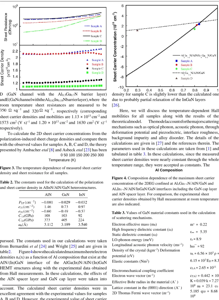
pursued. The constants used in our calculations were taken from Bernardini et al [24] and Wright [25] and are given in table2. Figure4showsthecalculatedmaximumsheetelectron densities ns(x) as a function of Al composition that exist at the AlN/(In)GaN interface of the AlGa(In)N/AlN/(In)GaN HEMT structures along with the experimental data obtained from Hall measurements. In these calculations, the effects of the AlN spacer layer and GaN cap layer were taken into account. The calculated sheet carrier densities were in excellent agreement with the experimental values for samples A, B and D. However, the experimental value of sheet carrier
density for sample C is slightly lower than the calculated one due to probably partial relaxation of the InGaN layers [26].
Here, we will discuss the temperature-dependent Hall mobilities for all samples along with the results of the theoreticalmodel. Themodelaccountsforthemajorscattering mechanisms such as optical phonon, acoustic phonon, through deformation potential and piezoelectric, interface roughness, background impurity and alloy disorder. The details of the calculations are given in [27] and the references therein. The parameters used in these calculations are taken from [1] and tabulated in table 3. In these calculations, since the measured sheet carrier densities were nearly constant through the whole temperature range, they were accepted as constants. The
Al Composition
Figure 4. Composition dependence of the maximum sheet carrier concentration of the 2DEG confined at AlxGa1−xN/AlN/GaN and
AlxIn1−xN/AlN/InGaN/GaN interfaces including the GaN cap layer
and AlN spacer layer. For comparison, the experimental sheet carrier densities obtained by Hall measurement at room temperature are also indicated.
Table 3. Values of GaN material constants used in the calculation of scattering mechanisms.
Electron effective mass (m0)
High frequency dielectric constant (ε0)
Static dielectric constant (ε0)
LO-phonon energy (meV)
Longitudinal acoustic phonon velocity (ms−1)
Density of the crystal (kgm−3) Deformation
potential (eV)
Elastic constants (Nm2)
Electromechanical coupling coefficient Electron wave vector (m−1)
Effective Bohr radius in the material (A˚ ) Lattice constant in the (0001) direction (A˚ ) 2D Thomas Fermi wave vector (m−1)
m∗ = 0.22 ε∞ = 5.35 εs = 8.9 hω¯ = 92 υL = 6.56 × 10³ ρ = 6.15 × 10³ E D = 8.3 cLA = 2.65 × 10¹¹ cTA2 = 0.442 × 10¹¹ K = 0.039 k = 7.27 × 10⁸ a B = 23.1 c0 = 5.185 qTF = 8.68 × 10⁸
results are shown in figure 5. The calculated total mobility as a function of lattice temperature is in very good agreement with the experimental data for all samples. The temperaturedependent Hall mobility revealed that the Hall mobilities in samples A (figure 5(a)), B (figure 5(b)) and C (figure 5(c)) are mainly determined by interface roughness scattering at low temperatures. As the temperature increases (above ∼100 K), acoustic phonon scattering in addition to the interface roughness becomes operative in the determination of the overall mobilities. At higher temperatures, the mobilities are limited by a combination of both interface roughness and optical phonon, and to a lesser degree, acoustic phonon scattering mechanisms.
On the other hand, as seen in figure 5(d), which shows the experimental and calculated temperature-dependent Hall mobilities of sample D, the high temperature (T > 240 K)
mobility is mainly determined by both acoustic and polar optical phonon scattering with increasing strength of the optical phonon component as the temperature increases to room temperature. At moderate temperature ranges, the acoustic phonon scattering through both deformation potential and piezoelectric interactions with nearly equal strength
dominate the Hall mobility. As the temperature decreases further, the mobility is characterized by the combination of all (except optical phonon) scattering mechanisms. Therefore, the low field transport in this sample is assumed to be nearly intrinsic. The weaknesses of extrinsic scattering mechanisms are indicative of a high-quality GaN channel with a low dislocationdensityandasmoothinterface. Thesameargument can be made on the transport characteristics of sample E, as discussed in [21].
To compare the transport properties in detail, the conduction band potential profiles and the spatial distribution of the amplitude of the electron wavefunctions are calculated by solving 1D nonlinear self-consistent Schrodinger–Poisson¨ equation [28]. The results are shown in figure 6. The material parameters of alloys for simulation were deduced using Vegard’s law and the layers were assumed to be
pseudomorphically grown. As seen in the figure, the spatial variation of the electron wavefunctions, particularly its penetration into the barrier, decreases due to the higher band offset of AlN. Keeping the carriers in the channel away from the scattering centers (the ternary barrier) results in effective suppression of the scattering due to alloy disorder for all Figure 5. The temperature evolution of the measured Hall mobility in comparison with the theoretical calculations including major scattering mechanisms for (a) sample A, (b) sample B, (c) sample C and (d) sample D.
Semicond. Sci. Technol. 25 (2010) 045024 S Gokden¨et al
samples. The unavoidable (intrinsic) scattering mechanisms associated with acoustic and optical phonons are mostly influenced by charge carrier density, effective well width at the heterointerface and the position of the Fermi level. As seen in figure 6, the pseudo-triangular potential wells are deeper for samples with the InGaN channel compared to the sample with the GaN channel only. In the calculation of the mobility limited by phonon scattering, we used the effective potential well widths deduced from the full width at half maximum of the electron wavefunctions.
Since the potential depth and hence the effective well width of samples A, B and C is almost the same, the mobility values purely limited by optical phonons are found to be the same for samples A and B (1556 cm2 (V s)−1), but lower than that of sample C (2057 cm2 (V s)−1) due to lower sheet carrier density of the latter. The effect of other scattering mechanisms (excluding the interface roughness) would be expected to give close mobility values as calculated. Therefore, the interface roughness scattering should be considered as the
Figure 6. The calculated conduction band potential profiles and spatial distribution of the amplitude of the electron wavefunctions for all samples.
main scattering mechanism limiting the mobility in these samples. In general, there are two parameters used in the calculation of the mobility limited purely by interface roughness scattering, namely the correlation length and the lateral size at the AlN/GaN interface, respectively. In the calculation, the root mean square (rms) roughness values obtained from AFM scans were taken as the lateral size parameter (). The correlation length was taken in the range of 5–25 nm [29] as a free parameter to fit the experimental mobility data. The mobility increases as decreases and increases and hence the larger the /, the smoother the interface. In this calculation, the effect of the sheet carrier density and the shifting of the centroid of the electron distribution toward the interface on the effectiveness of the interface roughness scattering [30] was also taken into account.
When the mobilities limited by interface roughness are compared for samples with InGaN channels, one can see the effectofthealloycompositionoftheAlInNbarrierlayeronthe AlN/InGaN interface. When the average lateral roughness ( or /) deduced from the mobility analysis is considered, the channel/barrier interface becomes smoother as the In content increases in the AlInN barrier. This helps to reduce the interface roughness scattering which results in higher electron mobility as seen in table 1. On the other hand, the interfaces of the samples with GaN channels only (samples D and E) are remarkably much smoother compared to the samples with InGaN channels when both and parameters are considered. ThelargerroughnessoftheAlN/InGaNinterfaces can be attributed to the fluctuations in In composition and layer thickness.
4. Conclusions
We studied the transport properties of AlInN/AlN/InGaN/ GaN heterostructures with different alloy compositions of AlInNbarrierlayersaswellasconventionalAlGaN/AlN/GaN and AlInN/AlN/GaN heterostructures using temperaturedependent Hall effect measurements. The scattering mechanisms were successfully analyzed and the dominant scattering mechanisms in the low- and high-temperature regimes were determined for all heterostructures. After studying the scattering mechanisms governing the transport properties of our samples, we concluded that the interface roughness is the main mobility limiting mechanism for the samples with InGaN channels. It has also been observed that the channel/barrier interface becomes smoother as the In content increases in the AlInN barrier. When these results are compared with the conventional GaN channel HEMTs, which have either AlGaN or AlInN barrier, mobilities are mainly limited by intrinsic scattering mechanisms such as optical and acoustic phonons indicating much smoother interfaces as deduced from AFM images. On the other hand, as far as the sheet resistance is concerned, we obtained the lowest sheet resistance value of 360 for sample B with the optimal In content of 18% in an AlInN barrier layer. This sheet resistance is comparable with that of the conventional HEMTs. Therefore, the sheet resistance of HEMT structures with InGaN channels can be reduced further once the AlN/InGaN/GaN interface is improved by optimizing the growth conditions. However, this is not an easy task due to the very different growth dynamics of the constitutive components. To overcome this problem, using a double heterostructure of Al(In)GaN/AlN/GaN/InGaN/GaN can be considered as another alternative design for the usage of the advantageous InGaN channel.
Acknowledgments
The VCU portion of this work has been funded by a grant from the US Air Force Office of Scientific Research under the
direction of Drs Kitt Reinhardt and Don Silversmith. The NANOTAM portion of this work is supported by TUBITAK under project numbers 104E090, 105E066, 105A005, 106E198 and 106A017 and the European Union under the projects EU-METAMORPHOSE, EU-PHOREMOST, EUPHOME and EU-ECONAM. One of the authors (EO) acknowledges partial support from the Turkish Academy of Sciences.
References
[1] Morkoc¸ H 2008 Handbook of Nitride Semiconductors and
Devices vols 1–3 (New York: Wiley-VCH)
[2] Xie J, Leach J H, Ni X, Wu M, Shimada R, Ozg¨ ur¨ U¨ and Morkoc¸ H 2007 Appl. Phys. Lett. 91 262102
[3] Miyoshi M, Egawa T, Ishikawa H, Asai K-I, Shibata T, Tanaka M and Oda O 2005 J. Appl. Phys. 98 063713
[4] Xie J, Ni X, Wu M, Leach J H, Ozg¨ ur¨ U and Morkoc¸ H 2007¨ Appl. Phys. Lett. 91 132116
[5] Gonschorek M, Carlin J-F, Feltin E, Py M A and Grandjean N 2006 Appl. Phys. Lett. 89 062106
[6] Lisesivdin S B, Acar S, Kasap M, Ozcelik S, Gokden S and Ozbay E 2007 Semicond. Sci. Technol. 22 543
[7] Smorchkova I P, Chen L, Mates T, Shen L, Heikman S, Moran B, Keller S, DenBaars S P, Speck J S and Mishra U K 2001 J. Appl. Phys. 90 3998
[8] Ambacher O et al 1999 J. Appl. Phys. 85 3222
[9] Cao Y and Jena D 2007 Appl. Phys. Lett. 90 182112
[10] Palacios T, Rajan S, Chakraborty A, Heikman S, Keller S, DenBaars S P and Mishra U K 2005 IEEE Trans. Electron
Devices 52 2117
[11] Kuzm´ık J 2001 IEEE Trans. Electron Devices 22 510
[12] Kuzm´ık J 2002 Semicond. Sci. Technol. 17 540
[13] Tulek R, Ilgaz A, Gokden S, Teke A, Ozturk M K, Kasap M, Ozcelik S, Arslan E and Ozbay E 2009 J. Appl. Phys.
105 013707
[14] Simin G, Hu X H, Taraku A, Zhang J P, Koudymov A, Saygi S, Yang J W, Khan A, Shur M S and Gaska R 2001 Japan.
J. Appl. Phys. 40 L1142
[15] Lanford W, Kumar V, Schwindt R, Kuliev A, Adesida I, Dabiran A M, Wowchak A M, Chow P P and Lee J-W 2004
Electr. Lett. 40 771
[16] Simin G, Koudymov A, Fatima H, Zhang J P, Yang J W, Khan M A, Hu X, Tarakji A, Gaska R and Shur M S 2002
IEEE Electron Device Lett. 23 458
[17] Tang J, Wang X, Xiao H, Ran J, Wang C, Wang X, Hu G and Jinmin L 2008 Phys. Status Solidi c 5 2982
[18] Palacios T, Chakraborty A, Heikman S, Keller S, DenBaars S P and Mishra U K 2006 IEEE Electron Device Lett 27 13
[19] Adivarahan V, Gaevski M E, Islam M, Zhang B, Deng Y and Khan M A 2008 IEEE Trans. Electron Devices 55 495
[20] Wang C X, Tsubaki K, Kobayashi N and Makimoto T 2004
Appl. Phys. Lett. 84 2313
[21] Teke A, Gokden S, T¨ ulek R, Leach J H, Fan Q, Xie J,¨ Ozg¨ ur¨ U, Morkoc¸ H, Lisesivdin S B and¨ Ozbay E 2009¨ New
J. Phys. 11 063031
[22] Hums C, Blasing J, Dadgar A, Diez A, Hempel T, Christen J,¨ Krost A, Lorenz K and Alves E 2007 Appl. Phys. Lett.
90 022105
[23] Asbeck P M, Yu E T, Lau S S, Sullivan G J, van Hove J and Redwing J 1997 Electron. Lett. 33 1230
[24] Bernardini F, Fiorentini V and Vanderbilt D 1997 Phys. Rev. B
56 R10024
[25] Wright A F 1997 J. Appl. Phys. 82 2833
[26] Chu R M, Zheng Y D, Zhou Y G, Gu S L, Shen B and Zhang R 2003 Opt. Mater. 23 207
[27] Gokden S, Baran R, Balkan N and Mazzucato S 2004 Physica E 24 249
Gokden S, Ilgaz A, Balkan N and Mazzucato S 2004 Physica E 25 86
[28] Birner S, Hackenbuchner S, Sabathil M, Zandler G, Majewski J A, Andlauer T, Zibold T, Morschl R, Trellaki A and Vogl P 2006 Acta Phys. Pol. A 110 111
[29] C¸orekc¸i S, Usanmaz D, Tekeli Z, ¸¨ Cakmak M, Ozc¸elik S¨ and Ozbay E 2008¨ J. Nanosci. Nanotechnol. 8
640
[30] Lisesivdin S B, Yildiz A and Kasap M 2007 Optoelectron.