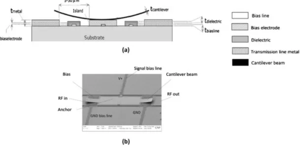
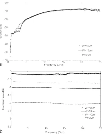
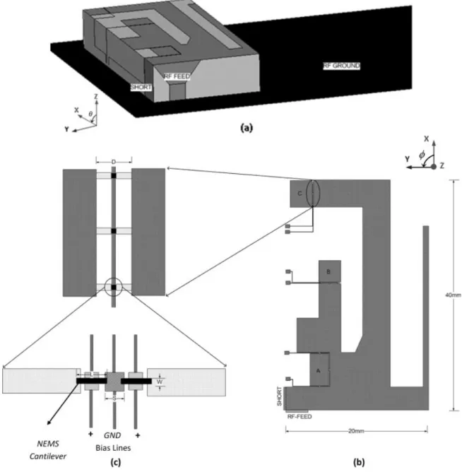
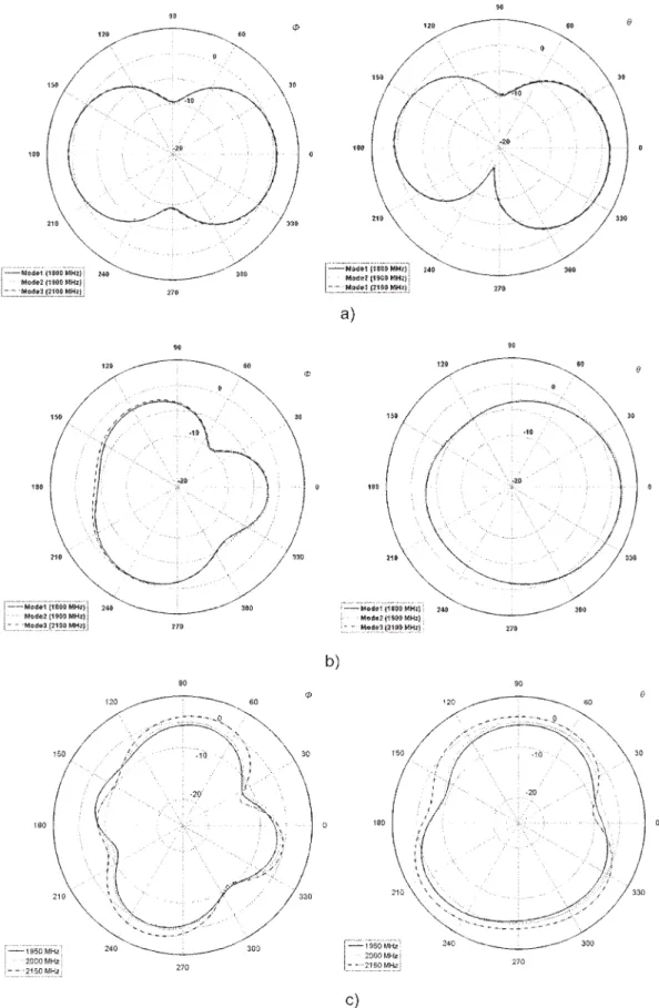
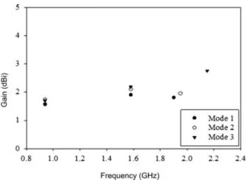
Nanoelectromechanical switches for reconfigurable antennas
Tam metin
Şekil
Benzer Belgeler
group, cytoplasmic immunoreactivity was observed in the hepatocytes throughout the liver sections (Fig. This immunoreactivity was stronger in hepatocytes located close to the
The cross-section problem of multiples of canonical line bundles over projective spaces is an important problem called generalized vector field problem. We have an interesting
From a structural realist perspective, improving relations between Turkey and Israel during the 1990s would not be unexpected given that the dynamics of regional politics in the
The model predicts that while both inflation and budget deficits are negatively associated with fiscal discipline, they may be positively associated with monetary discipline, proxied
We perform variational Monte Carlo calculations to show that bosons in a rotating optical lattice will form analogs of fractional quantum Hall states when the tunneling is
Along with rare Mendelian diseases, whole exome sequencing has also been applied to common and complex disorders to identify highly penetrant variants in familial forms of
By using the titles, duration and viewer- assigned ratings of more than two-thousand TED talks, we analyse whether the length of an information stream (talk duration) is related to
For the complexation studies of a series of bis-9-anthrylalkanes with a number of electron acceptors, we have prepared the title compound, (I), and carried out a single-crystal
