DESIGN AND DEVELOPMENT OF NOVEL LARGE
SCALE APPLICATIONS IN
MICRO/NANOPHOTONICS AND
NANOBIOTECHNOLOGY
A DISSERTATION SUBMITTED TO
MATERIALS SCIENCE AND NANOTECHNOLOGY PROGRAM OF THE GRADUATE SCHOOL OF ENGINEERING AND SCIENCE
OF BILKENT UNIVERSITY
IN PARTIAL FULFILLMENT OF THE REQUIREMENTS FOR THE DEGREE OF
DOCTOR OF PHILOSOPHY
By
Erol Özgür
August, 2014
I certify that I have read this thesis and that in my opinion it is fully adequate, in scope and in quality, as a thesis of the degree of Doctor of Philosophy.
………. Prof. Dr. Mehmet Bayındır (Advisor)
I certify that I have read this thesis and that in my opinion it is fully adequate, in scope and in quality, as a thesis of the degree of Doctor of Philosophy.
………. Prof. Dr. Engin Umut Akkaya
I certify that I have read this thesis and that in my opinion it is fully adequate, in scope and in quality, as a thesis of the degree of Doctor of Philosophy.
………. Assoc. Prof. Dr. Mehmet Özgür Oktel
I certify that I have read this thesis and that in my opinion it is fully adequate, in scope and in quality, as a thesis of the degree of Doctor of Philosophy.
………. Assoc. Prof. Dr. Mecit Yaman
I certify that I have read this thesis and that in my opinion it is fully adequate, in scope and in quality, as a thesis of the degree of Doctor of Philosophy.
………. Assist. Prof. Dr. Necmi Bıyıklı
Approved for the Graduate School of Engineering and Science:
………. Prof. Dr. Levent Onural
iv
ABSTRACT
DESIGN AND DEVELOPMENT OF NOVEL LARGE SCALE
APPLICATIONS IN MICRO/NANOPHOTONICS AND
NANOBIOTECHNOLOGY
Erol ÖzgürPh.D. in Materials Science and Nanotechnology Supervisor: Prof. Dr. Mehmet Bayındır
August, 2014
Developments in micro/nanophotonics and nanobiotechnology creates new opportunities regarding development of devices with unprecedented capabilities, which could improve human civilization substantially. On the other hand, a certain level of maturity in transforming these possibilities into reality still requires considerable efforts. One of the main problems of these novel technologies is that their practical know-how is so scarce that they could only be utilized within strictly determined laboratory conditions, and by highly sophisticated scientists.
This thesis focuses on large scale applications at the intersection of microphotonics and nanobiotechnology, and also in nanophotonics. On microphotonics side, optical microresonators with toroidal shape were successfully fabricated and optically integrated. Having an extremely high sensitivity towards perturbations in their environments, these microcavities could be used as biological sensors; however, they are also very sensitive for nonspecific interactions. Thus, a novel surface chemistry enabling bioconjugation of molecular probes without compromising their sensitivity and enhancing their selectivity was developed, based on methylphosphonate containing silane modification of the microtoroid surface. After this functionalization, microtoroids were used in biodetection in complex media.
v
Also, a macroscopic photodetection device composed on intrinsically aligned semiconducting selenium nanowires were demonstrated. This device could be considered as a novel and efficient demonstration of nanowire integration to the macroscopic world. Together with the research on biosensors, these are important large scale applications of emergent science of our age.
Keywords: Microtoroid, microphotonics, selectivity, sensitivity, surface chemistry,
nanobiotechnology, nanophotonics, semiconducting nanowires, large scale application.
ÖZET
MİKRO/NANOFOTONİK VE NANOBİYOTEKNOLOJİ İÇİN
YENİ YAYGIN UYGULAMALAR TASARLANMASI VE
GELİŞTİRİLMESİ
Erol ÖzgürMalzeme Bilimi ve Nanoteknoloji, Doktora Tez Yöneticisi: Prof. Dr. Mehmet Bayındır
Ağustos, 2014
Mikro/nanofotonik ve nanobiyoteknolojideki gelişmeler, insan uygarlığını büyük oranda değiştirebilecek, daha önce düşünülmemiş özelliklere sahip aygıtların ortaya çıkma ihtimalleri sunmaktadır. Bununla birlikte, bu ihtimalleri gerçekliğe dönüştürecek birikimin oluşması hala önemli bir çaba gerektirmektedir. Söz konusu yeni teknolojilerin en önemli sorunlarından bir tanesi, uygulamaları ile ilgili teknik bilginin azlığından dolayı, sadece çok iyi denetlenen laboratuvar koşullarında uzman araştırmacılar tarafından ilgili çalışmaların yürütülebilmesidir.
Bu tezin amacı, mikrofotoniğin nanobiyoteknoloji ile kesişiminde, ayrıca nanofotonik alanında yaygın uygulamaların geliştirilebilmesidir. Mikrofotonik alanı içinde toroid şekilli optik mikrorezonatörler üretilmiş ve ışıkla eşlenmişlerdir. Çevrelerindeki en ufak değişikliğe karşı bile çok hassas olan bu yapıların bu özelliğinden biyolojik sensörlerde faydalanılması amaçlanmakla beraber, bu durum beraberinde seçici olmayan etkileşmelere karşı da istenmeyen seviyede bir hassasiyet getirmektedir. Bu sorunun aşılması amacıyla hem protein dirençli hem de biyoeşlenebilir bir yüzey kaplaması geliştirilmiş, yüzeyi bu kaplamayla işlevselleştirilen mikrotoroidler, karmaşık ortamda biyolojik ölçüm yapmak için kullanılmıştır.
vii
Ayrıca, kendiliğinden düzenli yarıiletken selenyum nanoteller kullanılarak, makroskopik boyutta bir fotoalgılayıcı cihaz üretilmiştir. Bu cihaz, makroskopik dünyaya nanotel entegrasyonunda yeni ve verimli bir yöntem sunmaktadır. Biyosensör çalışması ile birlikte ele alındıklarında, çağımızın yükselen bilimi ile ilişkili önemli yaygın uygulamalar gösterilmiştir.
Anahtar kelimeler: Mikrotoroid, mikrofotonik, seçicilik, hassasiyet, yüzey kimyası,
Acknowledgement
First and foremost I would like to thank my academic advisor, Prof. Mehmet Bayındır, not only for the support and guidance he provided me throughout my dissertation, but also for the extremely valuable independence that he provided me during the course of my Ph.D., enabling me to utilize my creativity to its fullest extent, while simultaneously encouraging me to push the limits of the research furthermore. Being a member of Bayındır Research Group was a memorable experience, which I believe will continue to shape my future career as a scientist.
And also, all the faculty members, researchers, students and staff of UNAM-National Nanotechnology Research Center a priori deserve acknowledgement, appreciation and admiration. I would like to thank especially to Prof. Salim Çıracı for pioneering the establishment of such an invaluable research center.
I would like to express my acknowledgement to The Scientific and Technological Research Council of Turkey, TÜBİTAK, for the Ph.D. Scholarship I have benefited throughout my Ph.D.
Research is always a teamwork, and synergistic effect is ultimate in success. As a part of the team, I earnestly express that without my teammates, it would be impossible for me to accomplish even only a small part of what I have done. In particular, collaborating with Ozan Aktaş was one of my greatest opportunities in the course of my Ph.D. I do not even remember the number of problems, whether scientific or technical, that we solved together. An extremely talented researcher and natural born scientist like him is very difficult to be found elsewhere. Pelin Tören, although joined our group much later, also had an incredibly positive effect on both the route of my research, and my life. I am grateful for her resilient criticism that helped me to shift my point of view towards illumination for a myriad of times, and her sincere friendship. Lastly, I would like to thank one of the most open hearted person I have ever known, Ersin Hüseyinoğlu. Although his type of people have almost all became extinct, he stands there, self-confident, like a stone, providing constant trust, in research, and in life.
ix
Besides my teammates, here I also met other people that was also really fun to work with and talk to, and share thoughts and feelings. Adem Yildirim is one of them, whom I enjoyed much to be a colleague and a friend, and I hope we collaborate and meet every once in a while in future. I find people who really like talking quite amusing, and so is Bihter Dağlar. She is another person that I would like to see around and work together. I also want to express my gratitude to present and former Bayındır Research Group members: Fahri Emre Öztürk, Muhammad Yunusa, Tamer Doğan, Urandelger Tuvshindorj, Mehmet Kanık, Tural Khudiyev, Bekir Türedi, Pınar Beyazkılıç, Girayhan Say, Gökçen Birlik Demirel, Osama Tobail, Mostafa M. El-Ashry, İbrahim Yılmaz, Emel Gürbüz, Murat Dere, Dilara Öksüz, Hale Nur Çöloğlu, Seyit Ali Yaşar, Neşe Özgür, Mecit Yaman, Abdullah Tülek, Hakan Deniz, Hüseyin Duman, Muhammet Çelebi, Yunus Çetin, Duygu Akbulut, Kemal Gürel, Murat Celal Kılınç, Mert Vural, Enes Korkut, and Ahmet Ünal.
A person who deserves a special thank is my old friend Ali Aytaç Seymen. We, together, had a dream, and now we are on the verge of realizing it. I hope our harmony lasts for much longer times. I also would like to thank Bülend Ortaç for supporting our dream and believing in us. Lastly, from UNAM, I believe it would be incomplete without thanking Engin Umut Akkaya, Aykutlu Dana, Necmi Bıyıklı, Çağlar Elbüken, Mustafa Özgür Güler, Ali Kemal Okyay, Ayşe Begüm Tekinay, Urartu Şeker, Okan Öner Ekiz, Çağla Özgit Akgün, Ayşegül Abdelal, Melis Şardan, Aslı Çelebioğlu, Fatma Kayacı, Hakan Ceylan, Eda Çetinörgü Goldenberg, Rashad Mammadov, Sabri Alkış, Hasan Şahin, Handan Acar, Seymur Cahangirov, Selim Sülek, Enver Kahveci, Mustafa Güler, Zeynep Ergül Ülger, Semih Yaşar, Fikret Piri, Gökçe Çelik, Adem Saraç, Koray Mızrak, Emre Tanır, Mustafa Kemal Ruhi, and Burkan Kaplan.
And of course, my sweet family. Ekin Özge Özgür, my dear wife: Without her constant support and patience, nothing would be possible. She transformed me to the person I am now. She taught me love, and passion, and dignity. She taught me that being a good partner in life is more important than being a good scientist, and career is of no importance when family is the issue. She also gave me the most valuable present that I have ever had, our son, Erkin Ozan. I would not trade a thousand Ph.D. degrees for him. All I did, am doing and will do is for my family. Also, I would like to express my limitless thanks to my parents, Gülbahar and Bayram. Even if I am an
x
adult now for a long time, trying to stand on my very own feet, it is good to know that there is a place where I can always call “home”, no matter what happens.
As a last world, I dedicate my thesis to all graduate students. I wish they, the essence of research, will get what they deserve soon. I find it irrational and immoral that they are simultaneously indispensable and insignificant in front of the eyes of the scientific community. I believe things are changing to better, and as a scientist, I will definitely be on the side of progress regarding this issue.
Contents
ABSTRACT ... iv
ÖZET ... vi
Acknowledgement ... viii
Contents ... xi
List of Figures ... xiii
List of Tables ... xxii
Chapter 1 ... 1
Biosensing with Optical Microcavities ... 1
1.1 Introduction ... 1
1.2 Conventional Methods for Biodetection ... 2
1.3 Whispering Gallery Mode Microresonators for Biodetection ... 5
Chapter 2 Fabrication of Toroidal Microcavities ... 10
2.1 Photolithographic Patterning ... 10
2.2 Formation of Microdisks by Wet and Dry Etching ... 11
2.3 Formation of Microtoroids by CO2 Laser Reflow ... 13
Chapter 3 Optical Coupling to Microtoroids ... 15
3.1 Production of the Tapered Optical Fibers ... 15
3.2 Optical Coupling and Measurement Setup ... 20
3.3 Observation and Analysis of Whispering Gallery Modes ... 23
xii
4.1 Surface Chemistry for Simultaneously Protein Resistant and Bioconjugable
Surfaces ... 27
4.2 Coating and Characterization of Silica Surfaces ... 31
4.3 Demonstration of the Protein Resistance of THPMP Coated Silica Surfaces . 38 4.4 Covalent Protein Conjugation to the THPMP Functionalized Silica Surfaces 41 Chapter 5 Microtoroids as Biosensors with High Selectivity and Sensitivity .... 51
5.1 Construction of the Biosensing Setup ... 51
5.2 Analysis of the Data ... 53
5.3 Surface Modification of Microtoroids ... 54
5.4 Label-free Biosensing with Microtoroids with High Sensitivity and Selectivity ... 58
Chapter 6 Large Scale Integration of Nanowires as a Macroscopic Functional Device ... 65
6.1 Large Scale Nanowire Integration Strategies ... 65
6.2 Emergent Semiconductor Properties in Selenium Nanowire Arrays Fabricated by Direct Size Reduction Technique ... 68
6.3 Macroscopic Assembly of Indefinitely Long and Parallel Nanowires into Large Area Photodetection Circuitry ... 75
Chapter 7 Conclusions ... 89
Bibliography ... 91
xiii
List of Figures
Figure 1.1: Various types of optical microcavities with their corresponding 𝑄 and 𝑉. [6] Surface roughness is the primary source of the optical loss, determining the 𝑄. .. 6 Figure 1.2: Examples of biosensing with WGM type microresonators. (a) Detection of DNA single strands with microspheres functionalized with their complementary DNA. This sensor is capable of distinguishing single nucleotide polymorphisms. [11] (b) Detection of conformational changes of bacteriorhodopsin protein assembled over a microsphere. Bacteriorhodopsin contains the chromophore retinal, which changes conformation upon exposure to light. This leads a conformation change in bacteriorhodopsin, which could be detected as a shift in resonant wavelength. [13] (c) Single virus detection using microspheres. [12] (d) Detection of IL-2 protein using microtoroids, the time scale and the associated concentration-resonant wavelength shift graph. [14] ... 8 Figure 1.3: Schematic representation of biosensing with a toroidal microcavity. The interaction of the analyte with the microtoroid surface via targeting probes creates a shift in the resonant wavelength, which could be tracked in order to detect the amount of the interaction. ... 9 Figure 2.1: Optical microscopy images after the photolithography. (a) Image taken with a 5X objective. (b) Image taken with a 50 X objective. This perfect circularity could be attained with the proximity mode of the mask aligner. ... 11 Figure 2.2: 45° and side view of the microdisks after ICP etch. (a) 45° view of a fabricated microdisk for observing the circularity. (b) Side view of the microdisk, with a total tilt angle of 85°. The Si pillar could also be observed. There is a wedge shape at the circumference of the disk, related to the isotropic nature of BOE. ... 13 Figure 2.3: Components forming the microtoroid reflow setup. ... 14
xiv
Figure 2.4: SEM images of the microtoroids. Both top and side (75° tilted) views were investigated to comprehend the toroid morphology better. ... 14 Figure 3.1: Schematic representation of the basic components forming the fiber tapering setup. The light inside the fiber is also continuously monitored. ... 17 Figure 3.2: Transmission from the optical fiber during the fiber tapering. Transmission is given as a function of the change in the position of one of the motion controllers; therefore, the actual taper length is twofold. ... 18 Figure 3.3: Transmission spectra of a SMF28 fiber before (blue) and after (red) the tapering process. The transmission in the tapered fiber has a similar transmission pattern with the fiber before tapering, except a loss occurring during the tapering, demonstrating the adiabadicity of the tapering process. ... 19 Figure 3.4: SEM images of a tapered fiber. The fiber is uniform in diameter within a large length range (a), and submicron diameters could be reached. For instance, the taper diameter here is 750 nm (b). ... 20 Figure 3.5: Schematic representation of the optical measurement setup. The components are used simultaneously with a custom software to capture and record data. ... 22 Figure 3.6: Imaging optical coupling. Side (a) and top (b) views of optical coupling to microtoroids are given. Also, with the help of an IR camera, the optical coupling could be visualized. ... 23 Figure 3.7: Optical spectrum of coupled light into the microtoroids. (a) There are consecutive mode patterns separated by 𝐹𝑆𝑅. (b) Perpendicular polarizations show different resonance patterns. ... 24 Figure 3.8: A high resolution scan of a single resonant mode. A Lorentzian fit of the mode is also given in the figure. ... 26 Figure 4.1: Schematic representation of formation of simultaneously bioconjugable and protein resistant coating over silica. Piranha activated silica surface is first treated with methylphosphonate containing silane (1), which forms a protein resistant thin
xv
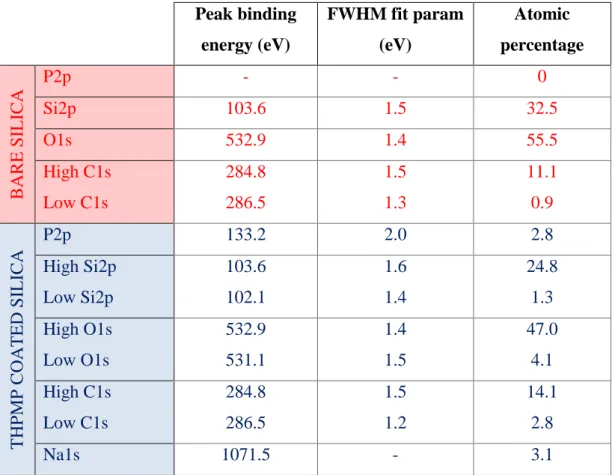
film. Methylphosphonates could be activated temporarily by using a cross-linker molecule (2). After the covalent attachment of proteins from their primary amines via these activated moieties (3), the coating reverts to its bio-inert state, besides being functionalized. ... 31 Figure 4.2: XPS survey spectra of the bare (a) and THPMP coated (b) silica surfaces. ... 33 Figure 4.3: Comparison of high resolution XPS scans of P2p, Si2p, O1s and C1s regions for bare silica and THPMP coated silica surfaces. Original data were given in blue lines, while fits for single peaks and envelopes were given in dashed and solid red lines, respectively. ... 35 Figure 4.4: CCD camera images of water droplets on the (a) piranha cleaned silica surface (2 x 2 cm) and (b) THPMP coated silica surface (0.5 x 0.5 cm) at room temperature. Droplet volume was 3 μl for both samples. ... 36 Figure 4.5: Surface topologies of bare (a) and THPMP coated (b) silica surfaces. Rms surface roughness increased after THPMP coating of silica surface. ... 37 Figure 4.6: 2D AFM images (1 x 1 μm) of the (a) bare silica, (b) THPMP coated silica given with line profiles and histograms. ... 37 Figure 4.7: XPS spectra for N1s of bare and THPMP coated silica surfaces after exposure to (a) BSA, (B) γ-globulin, (c) fibrinogen, and (d), lysozyme solutions. THPMP coating showed significant resistance to all tested proteins. The ratios of intensities (I0/ITHPMP) were calculated after background correction. ... 39 Figure 4.8: Ellipsometry measurements of nonspecific BSA adsorption over bare silica and THPMP coated silica surfaces. ... 40 Figure 4.9: High resolution XPS scan of N1s region for the EDC/NHS chemistry applied THPMP coated silica surface. Original data were given in blue lines, while fits for single peaks and envelopes were given in dashed and solid red lines, respectively. Components peaks (at 402.2 and 400.0 eV) verifies the existence of stable NHS-esters on surface. Full-width half-maxima of the component peaks at 402.2 and 400.0 eV, are 0.9 eV and 2.3 eV, respectively. ... 43
xvi
Figure 4.10: Confocal microscopy for quantitative detection of protein resistance. Nonspecific adsorption of FITC-BSA over piranha treated quartz surface (a) is almost diminished after THPMP coating (b). Covalent attachment, which produces comparable signal level to nonspecific adsorption, is possible by EDC activation (c), while THPMP coating can be reverted to its protein resistant original state later (d). The comparison of the fluorescence intensities (e) enables quantitative comparison of the amount of protein present over the surface. ... 45 Figure 4.11: High resolution XPS scans of P2p and N1s regions for the (a) EDC activated and (b) then recovered THPMP coated silica surface. Original data were given in blue lines, while fit for single peak was given in solid red line. P2p peak (solid red line) has full-width half-maximum of 2.0 eV. ... 46 Figure 4.12: Confocal microscopy images of quartz wafers functionalized with Cy5 labeled single strand DNA (a) and subsequently incubated in 1 mg/ml FITC-BSA (b). The fluorescence intensities of FITC (c) and Cy5 (d) does not show a significant difference between these two samples, demonstrating the bioconjugability and simultaneous protein resistance... 47 Figure 4.13: Surface topologies of covalently BSA conjugated silica surfaces with (a) 10 x 10 and (b) 1 x 1 µm scanned areas. 3D image on the left shows that the bioconjugated coating has a definite topography over a wide area. 3D AFM image on the right demonstrates that the bioconjugation follows the pattern of the THPMP coating, with a slightly but yet significantly increased rms surface roughness. ... 48 Figure 4.14: 2D AFM images of the covalently BSA conjugated THPMP coated silica surface with (a) 10 x 10 μm, and (b) 1 x 1 μm scanned areas given with line profiles and histograms. Scale bars are 2.5 μm and 250 nm, respectively. ... 49 Figure 4.15: Surface topology of the non-specifically bound BSAs onto piranha cleaned silica surface. Rms surface roughness was measured as 1.23 ± 0.19 nm. .... 50 Figure 5.1: Image of the biosensing setup. (a) The components of the biosensing setup, which are piezo stage and controller, tunable laser, powermeter or detector,
xvii
oscilloscope, and syringe pumps with appropriate tubing. (b) A close view of the biosensing platform. ... 52 Figure 5.2: Schematic representation of the biosensing in the microaquarium. The chip is fixed on the Plexiglas by tape. There are two holes drilled on the Plexiglas platform, for simultaneous infusion and withdrawal of liquids via the syringe pumps. (a) The microtoroids are optically coupled inside the microaquarium prior to experiment. (b) The analyte is infused and the liquid constituting the microaquarium is withdrawn simultaneously with the same rate in order to keep liquid volume constant. ... 52 Figure 5.3: A resonance dip recorded from optical coupling to a piranha treated microtoroid. After 15 min of treatment, no decrease in the 𝑄 was observed. ... 56 Figure 5.4: DIC and confocal images of only piranha cleaned (a,b) and THPMP coated (d,e) microtoroids. There is a significant fluorescence from the piranha cleaned microtoroid, while this signal is almost vanished from THPMP coated one, showing a significant reduction in nonspecific protein adsorption. The merged images of these microtoroids are also given (c,f). ... 57 Figure 5.5: Measurement of whispering gallery modes inside liquid media. There is a quite significant enlargement in the 𝐹𝑊𝐻𝑀 of the mode, representing a decrease in 𝑄. This effect occurs because H2O molecules around the microresonator absorb the light around 1550 nm to some extent. ... 59 Figure 5.6: Protein resistant characteristic of a surface modified microtoroid. (a) Time trace of the resonant wavelength shift after introduction of 0.1X FBS with an infusion rate of 5 µm/s. The graph starts at the point of the increase of the resonant wavelength. (b) The corresponding FBS concentration dependence of the resonant wavelength shift. ... 61 Figure 5.7: IL-2 measurement in PBS buffer. (a) Time trace of the resonant wavelength shift after introduction of IL-2 with an infusion rate of 5 µm/s in PBS. The graph starts at the point of the increase of the resonant wavelength. (b) The corresponding IL-2 concentration dependence of the resonant wavelength shift. ... 63
xviii
Figure 5.8: IL-2 measurement in PBS buffer with 0.1X FBS. The time trace of the functionalized microtoroid shows a significant shift after the infusion of the analyte in complex media. This shift is on the same order with the shift observed in PBS. A significant shift was not observed in the bare microtoroid, which could be anticipated, since the concentration of IL-2 in the analyte solution is more than four orders of magnitude lower that the total protein concentration. The decrease in the resonant wavelength with time could have occurred due to absorption of some constituents of FBS on the syringe and tube walls. ... 64 Figure 6.1: Schematic representation of iterative size reduction technique for nanowire production. A macroscopic preform containing the material of which the nanowire would be produced, encapsulated by a protecting polymer layer is prepared and then drawn in a custom built fiber tower. The resulting wires are cut into pieces and stacked together, and encapsulated again with the same polymer to obtain a second preform for a second thermal drawing step. This procedure could be repeated until nanowires of the desired size are obtained. During the process, the fiber diameter decreases, while the length and total number of micro and nanowires within the polymer encapsulated fiber increases. This method enables production of thousands of aligned and uniform nanowires of various material sets. ... 68 Figure 6.2: SEM image of the amorphous selenium nanowire array. The wires could be preserved axially ordered as they were produced within the encapsulating polymer layer. ... 70 Figure 6.3: Sizes and crystalline structure of selenium micro and nanowires produced by iterative thermal drawing. Step 1 and Step 2 microwires could be crystallized by thermal annealing, while pyridine treatment was required in order to crystallize the Step 3 nanowires. ... 71 Figure 6.4: SEM micrographs of crystallized selenium nanowires. (a) SEM image of highly ordered selenium nanowire array. The wires extend to microscopic lengths, while their diameters are in the order of nanometers. (b) SEM image of a single crystalline selenium nanowire. Although the surface has a roughness to some extent, the integrity of the wire is not compromised. ... 72
xix
Figure 6.5: Spiky shapes formed after overnight pyridine incubation of exposed amorphous selenium nanowires. ... 73 Figure 6.6: Size-dependent photoconductivity of selenium nanowires. The peaks occur when the light is on, while the conductivity decreases when the illumination is off. 74 Figure 6.7: Photoresponse of selenium micro and nanowires according to their sizes. The photoresponsivity increases with decreasing sizes. The data suggests that selenium nanowires could reliably be used with kHz modulation. ... 75 Figure 6.8: Macroscopic assembly of nanowires over a predefined circuitry. First step of nanowire integration to a macroscopic circuitry for large area photodetection is manual alignment and accommodation of polymer fiber arrays, each containing hundreds of nanowires embedded inside, over lithographically defined circuitry. A concept design of photodetection device resulting from macroscopic assembly of indefinitely long and endlessly parallel nanowires is given at the bottom. Nanowires are exposed over the metal electrode pairs as monolayers, forming pixels as photoconductive units, which are addressable by external readout circuits. Exposed light intensity can be deduced by applying a constant voltage across the pair of electrodes and measuring the change in conductance. ... 76 Figure 6.9: Schematic representation of nanowire based circuitry fabrication. After the nanowire arrays were properly placed over the electrical contacts, the polymer encapsulation was gently dissolved without disturbing the position of the nanowires. There, nanowires formed conduction channels over the electrodes. ... 78 Figure 6.10: High resolution transmission electron microscopy images of the selenium nanowires after crystallization. Fiber embedded nanowires were assembled over a TEM grid, and after removal of the polymer encapsulation, they were crystallized by exposing to an aqueous pyridine solution, 50% by volume, overnight. Pyridine reorganizes selenium atoms into crystalline form, while being diluted preserves the integrity of individual nanowires. The crystal structure could be (a) single crystal or (b) polycrystalline. ... 79
xx
Figure 6.11: SEM image of the large area nanowire device. (a) The electron microscopy image of crystallized selenium nanowires lying over ground and readout electrodes of the lithographically defined circuitry. A 3x3 pixel part of the device is shown here. Even though pixels are sparsely distributed on the circuitry, nanowire alignment over the electrode pairs of pixels can be easily accomplished. The limits of a device prepared by manual macroscopic alignment is defined only by photolithography. (b) SEM image of a single pixel, composed of hundreds of photoconductive selenium nanowires aligned over electrode pairs. Distance between a pair of electrodes is 10 micrometers. A high resolution SEM image of NW arrays can be seen in the inset. ... 80 Figure 6.12: Electrical characterization of a single nanowire array over the electrodes. (a) Photoconductive response of a nanowire based pixel under on-off modulated illumination of a broadband light source. Current data is normalized to dark current Io which is on the order of picometers. (b) Current-voltage characterization of one of the pixels for a static dark (blue) and bright illumination (red) showing ohmic behavior. Inset shows an individual pixel under applied voltage and illumination at constant intensity. ... 82 Figure 6.13: Capturing, displaying and identifying via large-area nanowire based photodetector circuitry. The circuitry is composed of a 10 x 10 pixel array over an area of 1 cm2, over which pixels have 1 mm separation. In order to create an image, dark field imaging was applied via passing white light through transparent parts of a shadow mask. The mask was prepared by printing alphabetic characters on transparent paper. The increase in conductivity regarding light exposure on the illuminated pixels were monitored and conditioned by the embedded software, and the information is then transferred to the computer via USB. After calibration of each pixel by a custom built application software, alphabetic characters were identified in the images captured by the device. ... 84 Figure 6.14: Large area nanowire photodetection circuitry. (a) Assembled selenium nanowires on photodetection circuitry and custom made readout electronics. (b) Software constructed image of 10 x 10 pixels after full exposure of the device to a light
xxi
source for static dark and (c) bright illumination. (d) Images of dark field illuminated alphabetic characters of “UNAM” captured by nanowire based pixel array. Blue pixels are dead pixels which can result from the imperfections of electrical contacts on the circuitry or of the nanowire alignment process. There are particularly two dead pixel columns, related to a slight misalignment of the nanowires over the pixel electrodes. ... 85 Figure 6.15: Capturing, displaying and identifying via large-area nanowire based photodetector circuitry. The circuitry is composed of a 10x10 pixel array over an area of 1 cm2, over which pixels have 1 mm separation. In order to create an image, dark field imaging was applied via passing white light through transparent parts of a shadow mask. The mask was prepared by printing alphabetic characters on transparent paper. The increase in conductivity regarding light exposure on the illuminated pixels were monitored and conditioned by the embedded software, and the information is then transferred to the computer via USB. After calibration of each pixel by a custom built application software, alphabetic characters were identified in the images captured by the device. ... 86
xxii
List of Tables
Table 4.1: XPS results of the bare and THPMP coated silica surfaces... 33 Table 4.2: Ellipsometry data regarding nonspecific BSA adsorption over bare (B1-3) and THPMP coated (T1-3) silica surfaces. The data are given with the corresponding standard deviation and mean square error values estimated through the analysis. .... 41 Table 5.1: Composition of FBS. In 0.1X FBS in PBS, the total protein concentration is in average 3.8 mg/ml, of which 2.3 mg/ml are albumins [77]. ... 62
1
Chapter 1
Biosensing with Optical Microcavities
1.1 Introduction
As humans we, similar to virtually all other animals, gather qualitative and quantifiable information from the universe via our highly sophisticated sensory organs, which evolved within millions of years, driven by the probabilistic and imperfect nature of life that also enabled our existence. The source of external stimuli, besides the environmental physical parameters such as temperature, moisture, light, etc., is mostly related to living organisms directly or indirectly, shaping the course of the evolution of life and; therefore, of the sensory organs, regarding the eminent phenomenon denominated as natural selection. The emergence of human civilization; however, with rapidly increasing communication and collaboration skills among human beings, required more objective and quantitative means of detection of the stimuli of any kind, notwithstanding the subjective nature of the sensory organs developed under the drive of evolution.
A sensor is an artificial tool for detection of a measurable quantity, and transduction of it into a comprehensible and interpretable signal. Among different types of sensors, biological sensors constitute an important branch, since the environment of any living organism consist of organic and also inorganic matter related to biological activity.
2
Due to the microscopic, even nanoscopic scales that life-related processes occur, proper biological sensing could still be described as an immature field of research. Despite huge efforts after atomic resolution in imaging was attained, and elaborate improvements in physical chemistry and biochemistry in the last fifty years, biosensing still has its own limitations. In an age, where single-photon and single atom measurements can be performed within appropriate technical infrastructure, accurate detection of single proteins or even single bacteria remain challenging, partly because of the complex interactions among life-related entities, and also for the unlimited diversity provided by the organic chemistry based background of life.
People require biosensors both for to understand and manipulate the life. Scientists demand better tools to analyze the molecular pathways, components and mechanisms of physiological and pathological phenomena. In order to comprehend the localization and distribution of the metabolites and also the interactions among them, molecular and cell biologists need fast and reliable tools suitable for multiplexed detection. Genetics and genomics researchers are seeking novel genetic and epigenetic screening methods. Evolutionary biologists try to understand polymorphisms and their distribution in the populations, while oncologists require sensors for quantifying and classifying cancer markers in order to detect pathologies at earlier stages. Microbiology studies are closely related to daily life, because food consumption for survival is actually far too risky without proper supervision, and current technology for food screening heavily depends on conventional tests that are too slow to take appropriate precautions except destruction of even minimally contaminated food. Last but not least, for security issues, i.e., against biological warfare, high sensitivity and selectivity biosensors are important demands of the contemporary society.
1.2 Conventional Methods for Biodetection
The biodetection tools can be divided into two broad categories: Methods that require labeling prior to detection, and label-free methods. Labeling for detection exploits the quantitatively observable materials that are able to produce a measurable
3
signal themselves or by external means, such as fluorescent molecules. Labeling is performed before detection; therefore, a priori information about the existence and the approximate amount of the target molecule is a prerequisite. Label-free methods are more flexible compared to the other methods, where detection precedes labeling, if any required. However, they require a more complex hardware for detection most of the times.
Fluorescent imaging constitutes the most diverse and wide branch of labeling before detection. Because of the diffraction limit in optics, it is impossible to detect targets smaller than the optical resolution limit of about a few hundred nanometers; however, most of the biological entities are much tinier. Fluorescent imaging enables researchers to detect even a few nanometer sized targets quantitatively, because it is straightforward to collect the fluorescence and amplify the signal by a photomultiplier tube (PMT) or charge coupled device (CCD) camera [1]. Although the exact localization of the target molecule still could be ambiguous, the quantity can be precisely estimated from the intensity of the signal. There is an increasing population of fluorescent probes specific to many different targets, and optics technology is improving to subdiffraction spatial and ultrafast temporal resolution. Fluorescent detection will remain as an indispensable tool, especially for basic science research.
One prevalent disadvantage of labeling is the requisite of a specific interaction between the label and the target, which is not always possible. Additionally, a quantifiable alteration in the characteristics of the labeling molecule is required in order to distinguish the interaction from the free form label. These disadvantages lead the development of the label-free methods, which some important examples are summarized below.
Immune system of mammals provides the largest and most well-established platform for label free detection, including but not restricted to various blotting methods and Enzyme-Linked Immunosorbent Assay (ELISA) [1]. Although some variations are under development, the high selectivity and specificity of antigen-antibody reaction is the gold standard for conventional biological detection. Antibodies are readily produced in laboratory animals or culture plates, where the spectacular diversification ability of the immunity related cells are exploited. The
4
resulting products are used for detection of not only proteins but many other biochemical species. After the bioconjugation among antibodies and their targets occur, different additional strategies, among which the mostly used is the utilization of non-specific fluorescent-chemiluminescent molecules, is used to measure the extent of the interaction quantitatively.
Major problem related to immunologic detection is that the minimum detectable quantity is far more than single molecule. Therefore, alternative methods for detection are being developed. Since the immunogenic interactions are incredibly selective and specific, related research focuses on revealing the minimum amount of these interactions possible. Rather than a subsequent labeling step that reduces the efficacy, alternative methods for detection of antigen-antibody interaction were introduced in recent years, among which surface plasmon resonance (SPR) and quartz crystal microbalance (QCM) are frequently utilized.
SPR depends on the excitation of the surface plasmons by light on metallic surfaces at a specific incident angle. Depending on the chemistry over the metal surface and the wavelength of the incident light, the resonant angle is altered. Researchers exploit this characteristic to determine the immunogenic interactions at the surface in situ. A thin layer of metal, mostly gold, coated substrate is conjugated with the targeting probes such as antibodies, and the analyte solution is passed over the surface. Any interaction among the antibodies and the target shifts the resonant angle proportional to the strength of the interaction. Therefore, quantitative information about the amount of the target, and also the reaction rates could be collected. Even though single-molecule detection is not attainable by SPR, the method provides a fast and reliable alternative to conventional methods [2].
Another promising method is QCM, where the oscillations occurring in a piezoelectric material, quartz, is used for detection. The frequency of the oscillation depends on the mass of the quartz plate, and any alteration in the mass shifts this frequency. When the target interacts with the antibodies, coated on the surface of the quartz plate in a similar fashion with SPR, the shift in the oscillation frequency could be transduced as a signal that reveals the binding [3]. This method is shown to detect very low quantities [4], but single molecule interactions have not been reported yet.
5
1.3 Whispering Gallery Mode Microresonators for
Biodetection
A resonator is a system that light continuously oscillates back and forth at specific wavelengths (or frequencies) depending on the size of the cavity constituting the resonator structure. The resonant wavelengths could be determined by the total path length, because the path length should be an integer multiple of the wavelength, providing the appropriate condition for constructive interference [5]. In order to obtain visible or near infrared (NIR) light oscillating inside a resonator, with distinguishable resonant frequencies produced by alternating integer multiples of the wavelength, the size of the resonator has to be in order of micrometers, which can be named as a microresonator.
One method to create a microresonator is to fabricate a circular path for the light, where light can travel via total internal reflection. Evanescent field can be used to couple light into such a cavity, and depending on the geometry and the quality of the fabrication, once coupled, light an remain in the cavity oscillating for a long time, when the lifetime of a photon is considered. This phenomenon, known as whispering gallery mode (WGM), is obtained in microresonators with a circular path [6].
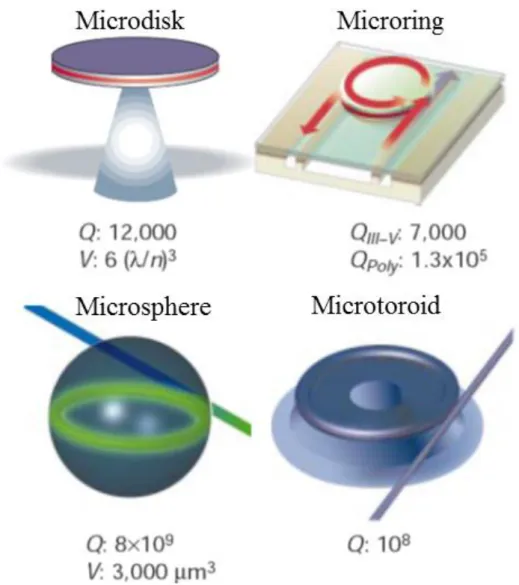
There are two main parameters that determine the efficacy of WGM type microresonators, which are quality factor (𝑄) and the mode volume (𝑉). 𝑄 determines how long the light will keep oscillating, and is directly related with all the loss mechanisms. 𝑉 is the volume in which light travels. The higher 𝑄 and the lover 𝑉 corresponds to the better microresonator [6].
Various geometries have been fabricated in order to attain WGM type microresonators, among which microspheres and microtoroids have the best characteristics. This is related to the fact that these microcavities are produced by surface tension created when the material they are formed of; i.e., silica, is melted. This greatly reduces their surface roughness, which is the primary reason of optical power loss in WGM microresonators. [7] Both microsphere and microtoroid geometries have very high 𝑄, in the order of 108-109; however, the mode volume of a
6
microtoroid is much lower, which provides many advantages besides on chip fabrication and thus easier integration to optoelectronic systems [8]. The advantage of a microsphere is that it can be fabricated much easier than a microtoroid, which requires long and detailed microfabrication processes. Different type of microresonators according to their geometry are given in Figure 1.1.
Figure 1.1: Various types of optical microcavities with their corresponding 𝑄 and 𝑉. [6] Surface roughness is the primary source of the optical loss, determining the 𝑄.
7
Microresonators, especially when equipped with high quality factors could be utilized as sensors with ultra-high sensitivity. Especially for biological sensing applications, microresonators provide incredible opportunities, including single molecule sensing [9]. Therefore, intensive research is being conducting in order to develop novel sensors using microresonators.
The ultra-sensitive sensing capability of the high 𝑄 microresonators depends on the perfect confinement of photons inside the cavity. Actually, biological samples have similar refractive index to the material that the microresonator have been fabricated, and the binding of even a single target entity with specific or non-specific interactions on the microresonator alters the path in which light travels, shifting the resonant wavelength towards red. The amount of the shift is proportional to the quantity of the interaction [10]. Since each photon inside the microresonator travels inside the resonator millions of times, this leads to a cumulative effect that enables the detection of even single molecule binding events.
Although nonspecific binding of the target readily occurs onto the material which the microresonators are fabricated, which is silica most of the times, the surface of these microresonators can be chemically modified in order to attain specificity. Modified surfaces containing detection probes such as antibodies provide highly sensitive biological and chemical sensors.
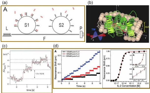
There are several important examples of biological sensors developed by utilization of the shift of the WGM of microresonators. Microspheres are shown to be used for detection of DNA [11], viruses [12], and detection of conformation changes of proteins coated on the microspheres are also demonstrated [13]. In another study, microtoroid sensors are shown to detect single protein binding events [14]. Figure 1.2 shows examples of WGM type microresonators as biosensors.
8
Figure 1.2: Examples of biosensing with WGM type microresonators. (a) Detection of DNA single strands with microspheres functionalized with their complementary DNA. This sensor is capable of distinguishing single nucleotide polymorphisms. [11] (b) Detection of conformational changes of bacteriorhodopsin protein assembled over a microsphere. Bacteriorhodopsin contains the chromophore retinal, which changes conformation upon exposure to light. This leads a conformation change in bacteriorhodopsin, which could be detected as a shift in resonant wavelength. [13] (c) Single virus detection using microspheres. [12] (d) Detection of IL-2 protein using microtoroids, the time scale and the associated concentration-resonant wavelength shift graph. [14]
Figure 1.3 shows a schematic representation of biodetection with toroidal microresonators with an appropriate surface chemistry.
9
Figure 1.3: Schematic representation of biosensing with a toroidal microcavity. The interaction of the analyte with the microtoroid surface via targeting probes creates a shift in the resonant wavelength, which could be tracked in order to detect the amount of the interaction.
Specificity is definitely as critical as sensitivity when a sensor is considered, since lack of differentiation of the target from any other species, namely false positives, could be as misleading as false negative results, which are related to the detection limits. Provided that the ultimate detection at single molecule level, by elaborate utilization of various targeting probes and an advanced level of surface chemistry, has been attained using microresonators, the remaining challenge is to increase the specificity of the detection, in order to enable these optical microcavities to be utilized as sensors reliably.
The specificity issue remains ambiguous in the literature, which can be tolerated since the field is rather new, and study in order to transform these highly sensitive sensors into detection tools with also high specificity will probably have important impact in related area. Surface chemistry have been enabling novel methods for highly specialized functional surfaces, and utilization of the surface modifications could enable the realization of high specificities associated with better sensors. Therefore, research on surface modified microresonators for simultaneously high sensitivity and specificity biological sensing could be considered as an important area of study.
10
Chapter 2
Fabrication of Toroidal Microcavities
2.1 Photolithographic Patterning
The fabrication of microtoroids begins with patterning of substrates with photolithography. During this research, 4 inch silicon wafers with thermal oxide layers grown on their top were utilized, and various oxide thicknesses were evaluated (University Wafers and Addison). The best fabrication results were obtained with an oxide thickness of 2 µm. Before photolithography, wafers were diced into 20 x 20 mm squares using a dicing saw (Disco), and each square chip was treated independently. After the substrates were cleaned with acetone, isopropanol and deionized (DI) water, respectively, they were spin coated first with HMDS at 4000 rpm for 45 s with a spin coater (Laurell), and then with the photoresist, AZ4533 again with the same parameters, to obtain a nominal photoresist thickness of 3.3 µm. Following a soft bake at 110 °C for 50 s on a hot plate, the photoresist was patterned using a 5 inch2 chromium patterned mask containing circular features, drawn with the commercial software L-Edit, and produced by a mask writer (Heidelberg Instruments). The exposure dose is 80 mJ/cm2, where also the proximity mode of the mask aligner (EVG620) is used with a proximity of 200 µm, in order to minimize the nanometer scale non-uniformities in the circularity, exploiting the diffraction of light at far field. After the exposure, the photoresist was developed using AZ400K developer with a
11
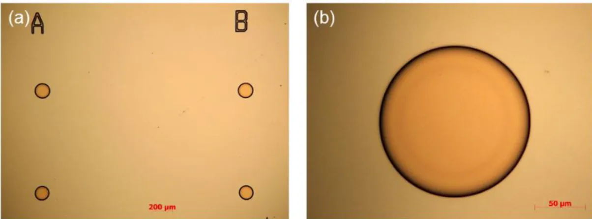
developer:H2O ratio of 1:4, for approximately two minutes. Following inspection of the disks with an optical microscope (Zeiss), the circular photoresist patterns were hard baked at 120 °C for 50 s (Figure 2.1).
Figure 2.1: Optical microscopy images after the photolithography. (a) Image taken with a 5X objective. (b) Image taken with a 50 X objective. This perfect circularity could be attained with the proximity mode of the mask aligner.
2.2 Formation of Microdisks by Wet and Dry Etching
Microtoroid fabrication process requires the etching of both the thermal oxide layer and the silicon substrate, where selectivity is the most important issue. The silicon oxide could be etched either by wet or dry etching methods, and both methods have their advantages and disadvantages. Inductively coupled plasma (ICP) etching could be used in order to have very anisotropic etch of the oxide. In this procedure, O2 (30 sccm) and CHF3 (100 sccm) gases are used with the forward coil power of 250 W and forward platen power of 30 W using a low frequency RF platen (380 kHz), at 50 mTorr using an ICP etch system (STS). The drawback of this method is that the etch rate is quite low (ca. 20 nm/s), and prolonged exposure to plasma damages the photoresist during etching. Wet etching, on the other hand, is performed with a 7:1 mixture of NH4F:HF, buffered oxide etch (BOE), where ammonium fluoride provides a buffer for hydrofluoric acid and prevents it from reacting with the oxide vigorously, in which the
12
photoresist is damaged by fast emission of gases during the chemical reaction. However, since this is an isotropic process, a wedge shape occurs, which becomes more apparent when the oxide thickness increases. After an optimization of these processes, we decided to use buffered HF for the etching of the oxide layer. The etch rate was ca. 60 nm/min, and the substrate with 2 µm oxide thickness was etched for 35 min to reveal silica disks over the silicon.
The next step was the isotropic etch of the silicon in order to obtain silica disks standing on silicon pillars. Prior to this step, the wafers were diced once more to obtain rectangles with sizes of 2 mm x 20 mm, each having a column of microdisks with varying sizes, in order to facilitate the coupling of light with a tapered fiber, and also more efficient use of microtoroids during surface treatment. ICP with SF6 gas (130 sccm) was used with coil forward power of 600 W and platen forward power of 8 W with a high frequency RF platen (13.56 MHz), at 50 mTorr. The vertical etch rate was measured as ca. 1 µm/min, while the lateral etch rate was observed to be ca. 0.5 µm/min. The optimized etch time was found to be 22.5 min, because shorter etch times led to the formation of microdisks with short undercuts that make them harder to reflow, while longer etch times created microdisks with non-uniformities in their pillar circularity, which causes problem in subsequent toroid shape. This could be explained by the fact that longer etch times damages the photoresist, and since SF6 plasma has a low selectivity for silica over silica, it harms the edges of silica microdisk, affecting the isotropicity of the silicon etch. XeF2, which has an extremely higher Si:SiO2 selectivity is often used for this process [15], while we observed that SF6 plasma created comparable results.
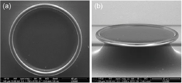
As a last step, the remaining photoresist is cleaned by using a mixture of O2 (30 sccm) and N2 (5 sccm) with 400 W RF power at a plasma cleaner (Asher) for 45 min. The scanning electron microscopy (SEM) (FEI Nova NanoSEM) images of the microtoroids are given in the Figure 2.2. In order to facilitate imaging from the sides, a SEM stub with 45° tilt was used, and the SEM stage was further tilted.
13
Figure 2.2: 45° and side view of the microdisks after ICP etch. (a) 45° view of a fabricated microdisk for observing the circularity. (b) Side view of the microdisk, with a total tilt angle of 85°. The Si pillar could also be observed. There is a wedge shape at the circumference of the disk, related to the isotropic nature of BOE.
2.3 Formation of Microtoroids by CO
2Laser Reflow
The rectangular wafer containing the microdisk array is clamped vertically on a small flip 2-axis motion stage for CO2 laser reflow. A He-Ne laser at 633 nm (Thorlabs) was used as a pilot light. The beam from a CW operating CO2 laser at 10.6 µm (Coherent) was focused over the microtoroids using a ZnSe plano-convex lens. Typical laser powers used were within the range of 12-20 W. Laser was controlled by a custom developed software. The reflow process was monitored by a charge coupled device (CCD) camera (Hitachi) equipped with a 10X plan apochromatic long working distance objective (Mitutoyo) and Zoom 70XL Optical System (Qioptiq). After the position of the microtoroid was aligned to the beam center, as observed with the pilot light, the flip mirror was folded to enable CO2 laser beam to interact with the microdisk. Figure 2.3 shows the reflow setup.
14
Figure 2.3: Components forming the microtoroid reflow setup.
Since silica has a much higher absorption for CO2 laser beam with the wavelength of 10.6 µm, it creates a high temperature that causes the melting of the silica. The silicon pillar, acting as a heat sink, leads to formation of a microtoroidal shape with a very low surface roughness [8]. The SEM images of the microtoroids are given in Figure 2.4.
Figure 2.4: SEM images of the microtoroids. Both top and side (75° tilted) views were investigated to comprehend the toroid morphology better.
15
Chapter 3
Optical Coupling to Microtoroids
3.1 Production of the Tapered Optical Fibers
Among various methods for coupling light into WGM microresonators such as free space [16] or prism coupling [17], and tapered fiber coupling, tapered optical fibers are the most prominent in terms of coupling efficiency [18]. Tapered optical fibers are generally produced by heating a particular zone of the silica fiber up to its softening temperature and pulling the fiber sides towards opposite directions simultaneously. The most important characteristic of a tapered fiber is adiabadicity, which is inversely correlated to the optical loss observed after the tapering process. In an adiabatically tapered fiber, transmission values higher than 99% could be observed [19]. The adiabadicity depends on the taper length, which longer tapers provide higher adiabadicity [20]. Although it is possible to etch fibers to form tapers using silica etchants such as HF [21], the best results are obtained by heating fibers by various means. Unlike etched fibers, where only the core of the fiber remains after tapering, when the fiber is tapered by simultaneously heating and pulling the fiber apart, the core of the fiber gradually diminishes, and at the taper region where the diameter is minimum, the optical wave inside the fiber is guided only by the remaining core region [20]. In case of uniform heating, the taper profile could be deduced from the formula below:
16 𝑟(𝑧) = 𝑟0𝑒−𝑧 𝐿⁄ 0
where 𝑟(𝑧) is the radius of the fiber at the distance 𝑧, which is the distance from the tapering center, and 𝐿0 is the length of the hot zone [20]. One important outcome of this formulation is that the taper length mainly depends on the length of the hot zone, provided that the hot zone is kept constant and uniform in terms of length and temperature.
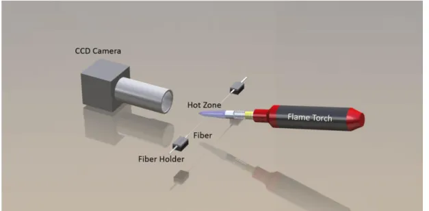
During our research we have tested various methods for fiber tapering including HF etch, CO2 laser heating prior to HF etch, CO2 laser alone, propane/butane torch, and hydrogen torch. The most effective tapering was observed with hydrogen torch used as a heating source. The tapering setup used in this research, as schematically represented in Figure 3.1 consists of several optical and mechanical elements. We have coupled SMF28 optical fibers to the output of a laser operating at 1550 nm (Santec TLS-510) and to the signal input of an optical powermeter (Newport 1935C) using mechanical fiber splicers (Thorlabs). The output intensity of the laser was monitored continuously during the tapering. We used two reciprocal linear motion stages (Newport) driven by an ESP motion controller (Newport). Laser, powermeter and linear stages were controlled simultaneously by a custom built software developed in C#. The tapering process was also continuously observed by a CCD camera equipped with a 10X plan apochromatic long working distance objective.
17
Figure 3.1: Schematic representation of the basic components forming the fiber tapering setup. The light inside the fiber is also continuously monitored.
Monitoring of optical output enables us to observe the alterations in the wave guiding characteristics during the fiber tapering process, as previously described in the literature [22]. Initially, the light travels within the core, which is single mode core-guided operating regime. During the tapering, the fiber first enters into taper multimode operating regime, and finally when the diameter approaches to the order of the wavelength, it enters into taper single mode operating regime. The fluctuations during taper multimode operating regime occurs because although the tapered region supports multiple modes, the rest of the fiber is still single mode, therefore it could not guide the modes formed at the tapered region. Figure 3.2 shows a typical fiber tapering process, where we typically obtain transmissions higher than 95% using our fiber tapering system. Figure 3.3 shows the transmission spectrum of a fiber before and after fiber tapering, demonstrating the adiabadicity of our fiber tapering process. Also, in Figure 3.4 there are SEM images of a tapered optical fiber.
18
Figure 3.2: Transmission from the optical fiber during the fiber tapering. Transmission is given as a function of the change in the position of one of the motion controllers; therefore, the actual taper length is twofold.
19
Figure 3.3: Transmission spectra of a SMF28 fiber before (blue) and after (red) the tapering process. The transmission in the tapered fiber has a similar transmission pattern with the fiber before tapering, except a loss occurring during the tapering, demonstrating the adiabadicity of the tapering process.
20
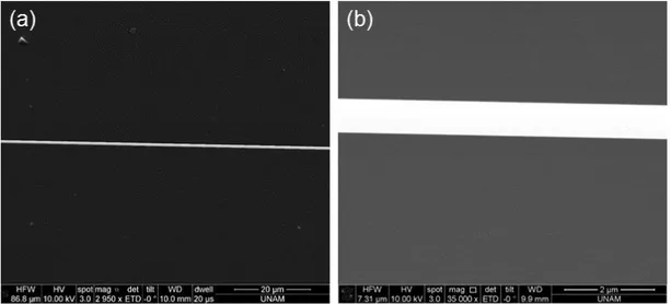
Figure 3.4: SEM images of a tapered fiber. The fiber is uniform in diameter within a large length range (a), and submicron diameters could be reached. For instance, the taper diameter here is 750 nm (b).
3.2 Optical Coupling and Measurement Setup
As mentioned in the previous section, light is coupled into microtoroids by using tapered fibers. While the light is guided through the taper region, an evanescent field traveling in the air around the fiber occurs. If this evanescent field encounters a medium with a similar refractive index, the light could be coupled into and out of the medium. When this medium is a resonator; i.e., a constructive interference of light occurs within that medium, the light is coupled into this resonator as resonant modes, which could be observed as dips in the transmission spectrum of the waveguide. Since the light travels within the microresonator as a result of total internal reflection, the constructive interference condition depends on the optical path length, which is the circumference of the microcavity, the wavelength of the coupled light, and effective refractive index of the resonator according to the following formulation [5]:
𝑚𝜆𝑚 = 2𝜋𝑟𝑛𝑒𝑓𝑓
Here, 𝑚 stands for mode number, an integer that satisfies the resonance condition, 𝜆𝑚 is the corresponding resonant wavelength, 𝑟 is the radius of the microresonator, and 𝑛𝑒𝑓𝑓 is the effective refractive index of the mode coupled into the microresonator,
21
depending on the propagation of light within the cavity, which differs from bulk material. 𝑛𝑒𝑓𝑓 is also essential for one of the two important phenomena regarding the optical coupling into all WGM microresonators, which are phase matching and critical coupling. Phase matching occurs when effective refractive indices of the waveguide and the microresonator have similar values. The refractive index of a waveguide having dimensions on the order of the wavelength of the light inside, similar to of a WGM microresonator, differs from the bulk material. The effective index decreases with decreasing taper diameter. The effective index of the WGM resonator, on the other hand, depends on its radius 𝑟, and it also decreases with decreasing resonator size [18]. Effective indices, therefore phase matching condition, could be calculated both analytically and numerically, and also phase matching could be determined empirically by changing the position of the microresonator with respect to taper diameter. Especially in complex geometries such as microtoroids, where there are less symmetry compared to spheres, numerical methods and empirical determination becomes more feasible. When phase matching condition is satisfied, all the optical power could be transferred within the microresonator. The second important condition regarding optical coupling to WGM microresonators is coupling efficiency, which depends mainly to the distance between tapered fiber and the microresonator, but also the taper diameter. There are three conditions that could occur with respect to coupling efficiency, which are undercoupling, critical coupling and overcoupling. The critical coupling occurs at the distance where all the optical power is transferred into the microresonator, which could also be determined experimentally [18].
The optical coupling setup used in this research consists of a tunable external cavity laser operating around 1550 nm (Santec TLS-510), a powermeter (Newport 1935C) or a 1.2 GHz InGaAs FC/PC-Coupled Photodetector, 800 - 1700 nm (Thorlabs), depending on the measurement, an oscilloscope acquiring data from analog output of the laser and powermeter or photodetector (Tetronix TDS-1012B), a 3-axis closed loop piezo stage (Thorlabs Nanomax TS) driven by a piezo controller (Thorlabs) on which an adjustable height, pitch and roll platform (Thorlabs) is mounted, and two optical microscopes enabling top and side imaging of the optical coupling. Laser, powermeter, and oscilloscope were controlled by a custom built software developed in C#, while
22
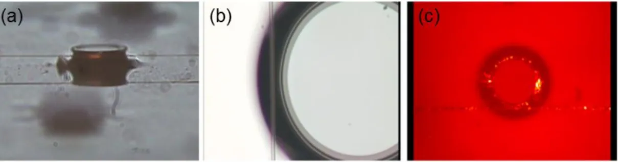
piezo controller could be used either manually or with the same software as well. The laser was tuned continuously within a predefined wavelength range between 1510 and 1620 nm, with a constant sweep rate that could be varied from 1 nm/s to 100 nm/s, and the voltage signal depending on the amount of tuning was tracked by the oscilloscope. The other channel of the oscilloscope simultaneously tracked the voltage signal from the powermeter, and the software recorded and also plotted these signals. The schematic representation of the optical measurement system is given in the Figure 3.5, and the images of a coupled microtoroid, as well as coupling observed with an infrared (IR) camera (Xenics) connected to our microscope system is given in Figure 3.6.
Figure 3.5: Schematic representation of the optical measurement setup. The components are used simultaneously with a custom software to capture and record data.
23
Figure 3.6: Imaging optical coupling. Side (a) and top (b) views of optical coupling to microtoroids are given. Also, with the help of an IR camera, the optical coupling could be visualized.
3.3 Observation and Analysis of Whispering Gallery Modes
As mentioned above, the coupling into the microresonators occurs as resonant modes, which depend on the interference condition. The polarization of the light is also important, and various TE and TM modes could be controlled by a manual polarization controller (Thorlabs FPC030). When a large wavelength range is scanned for optical resonances, a definite pattern of whispering gallery modes could be observed. The mode spectrum consists of these repeated patterns, separated by a distance denominated as free spectral range (𝐹𝑆𝑅) and calculated as following:
𝐹𝑆𝑅 = 𝜆 2 2𝜋𝑟𝑛𝑒𝑓𝑓
Each pattern represents an individual resonance condition, determined by consecutive values of the integer 𝑚 [23]. Provided that a plane polarized light is coupled into the microresonator, which could be accomplished by the polarization controller, several resonances could be observed in each pattern, representing modes of different orders. One distinct advantages of the microtoroids is that most of the higher order modes are suppressed due to the geometrical restrictions compared to
24
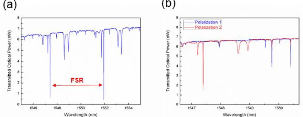
spheres. Figure 3.7 shows a spectrum of a microtoroid with several mode patterns separated by 𝐹𝑆𝑅, and a spectrum of a set of modes of different orders at perpendicular polarizations controlled by the paddle acting as a half wave plate. In order to minimize the instability caused by thermal effects, the power of the laser was kept at the order of nWs.
Figure 3.7: Optical spectrum of coupled light into the microtoroids. (a) There are consecutive mode patterns separated by 𝐹𝑆𝑅. (b) Perpendicular polarizations show different resonance patterns.
When each resonance dip is investigated individually, they provide another important information regarding the microresonator, which is the quality factor (𝑄). 𝑄 represents the amount of power that could be stored within the cavity. With an increasing 𝑄, the full width half minimum (𝐹𝑊𝐻𝑀) of the resonance becomes smaller, and the relation between 𝑄 and 𝐹𝑊𝐻𝑀 could be described as below [12, 24]:
𝑄 = 𝜆 Δ𝜆
where Δ𝜆 represents the 𝐹𝑊𝐻𝑀. While there are other more precise methods for measuring 𝑄 such as cavity ring down [8] or ringing [25], the formula above provides a reasonable estimate.
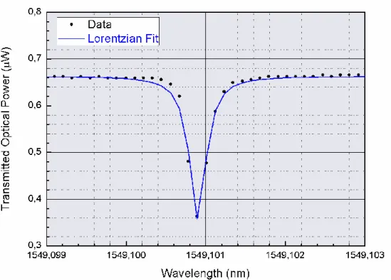
Although laser is tuned around the resonance continuously to observe WGM resonances, since the oscilloscope collects discrete data points, it is necessary to fit the data, which could be fitted to a Lorentzian function [26-28]. Physically, the
25
transmission intensity from the tapered fiber around a WGM resonance could be calculated accurately from the Lorentzian of the angular frequency 𝜔 as:
𝐹(𝜔) = 𝑇𝑖−
𝐴
(𝜔 − 𝜔0)2+ (𝐹𝑊𝐻𝑀 2 )2
where 𝑇𝑖 is the optical transmission without optical coupling, 𝐴 is the amplitude parameter of the coupling, and 𝜔0 is the resonant frequency. Since this function is in the frequency domain, 𝐹𝑊𝐻𝑀 should also be considered in terms of frequency. Yet, although not exactly Lorentzian, because the relation of 𝜆 with 𝜔 is not linear as shown below:
𝜆 =2𝜋𝑐 𝜔
the shape of the resonant mode in transmission spectrum in wavelength domain still resemble a Lorentzian function; therefore, the equation used in the calculations was:
𝐹(𝜆) = 𝑇𝑖−
𝐴
(𝜆 − 𝜆0)2+ (𝐹𝑊𝐻𝑀 2 )2
where 𝜆0 is the the resonant wavelength. In this notation, 𝐹𝑊𝐻𝑀 is also in the terms of 𝜆.
By a script performing nonlinear regression in MATLAB, it is possible to perform Lorentzian fit numerically and obtain the value of 𝑄 (Figure 3.8). As calculated from this Lorentzian fit, 𝑄 is 3.95 x 10⁶.