CHEMICALLY SPECIFIC DYNAMIC
CHARACTERIZATION OF
PHOTOVOLTAIC AND
PHOTOCONDUCTIVITY EFFECTS OF
NANOSTRUCTURES BY X-RAY
PHOTOELECTRON SPECTROSCOPY
A THESISSUBMITTED TO THE GRADUATE PROGRAM OF MATERIALS SCIENCE AND NANOTECHNOLOGY
AND THE INSTITUTE OF ENGINEERING AND SCIENCES OF BILKENT UNIVERSITY
IN PARTIAL FULLFILMENT OF THE REQUIREMENTS FOR THE DEGREE OF
MASTER OF SCIENCE
By
Okan Öner EKİZ July, 2010
i I certify that I have read this thesis and that in my opinion it is fully adequate, in scope and in quality, as a thesis for the degree of Master of Science.
Prof. Dr. Salim ÇIRACI (Supervisor)
I certify that I have read this thesis and that in my opinion it is fully adequate, in scope and in quality, as a thesis for the degree of Master of Science.
Res. Assist. Prof. Dr. Aykutlu DANA (Co-supervisor)
I certify that I have read this thesis and that in my opinion it is fully adequate, in scope and in quality, as a thesis for the degree of Master of Science.
Approved for the Institute of Engineering and Sciences:
Prof.Dr. Levent ONURAL
Director of Institute of Engineering and Sciences
iii
ABSTRACT
CHEMICALLY SPECIFIC DYNAMIC
CHARACTERIZATION OF PHOTOVOLTAIC AND
PHOTOCONDUCTIVITY EFFECTS OF
NANOSTRUCTURES BY X-RAY PHOTOELECTRON
SPECTROSCOPY
Okan Öner EKİZ
M.S. in Graduate Program of Materials Science and Nanotechnology Supervisor: Prof. Dr. Salim ÇIRACI
July, 2010
X-Ray Photoelectron Spectroscopy is a widely used characterization method for chemical analysis of surfaces. In this thesis, We report characterization of photovoltaic and photoconductivity effects on nanostructured surfaces through light induced changes in the X-ray photoelectron spectra (XPS). The technique combines the chemical specificity of XPS and the power of surface photovoltage spectroscopy (SPV), with the addition of the ability to characterize photoconductivity under both static and dynamic optical excitation. A theoretical model that quantitatively describes the features of the observed spectra is presented. We demonstrate the applicability of the model on a multitude of sample systems, including homo- and heterojunction solar cells, CdS nanoparticles on metallic or semiconducting substrates, and carbon nanotube films on silicon
substrates. A-Si/c-Si heterojunction solar cell is fabricated to characterize photovoltage generation in a nanostructured solar cell. Cadmium Sulfide (CdS) nanoparticles were synthesized by a solvo-thermal route. Both Multi Wall Carbon Nanotube (MWCNT) and Single Wall Carbon Nanotube (SWCNT) films were characterized with different substrates by XPS. Raman Microscopy, EDS, SEM, XRD, SAXS are used to characterize the samples and solar cells.
Keywords: X-ray photoelectron spectroscopy , carbon nanotubes , cadmium sulfide , silicon , dynamic characterization , surface photovoltage , photoconductivity , semiconductor nanoparticles , photovoltaics
v
ÖZET
Nanoyapıların Fotovoltaik ve Fotoiletkenlik
Özelliklerinin X-Işını Fotoelektron
Spektroskopisi ile Kimyasal Olarak Hususi
ve Dinamik Olarak Karakterizasyonu
Okan Öner EKİZ
Tez Yöneticisi: Prof. Dr. Salim Çıracı
Yüksek Lisans, Malzeme Bilimi ve Nanoteknoloji Bölümü Temmuz, 2009
X-Işını Fotoelectron Spektroskopisi, yüzeylerin kimsalar analizi için bilinen ve yaygın olarak kullanılan bir yöntemdir. Bu tez çalışmasında, nano-yapılandırılmış malzemelerin fotovoltaik ve fotoiletkenlik özelliklerinin X-Işını Fotoelektron Spektrası üzerindeki etkilerinin karakterizasyonu çalışılmıştır. Bu teknik, X-Işını Fotoelektron Spektroskopisinin kimyasal özgüllüğü ile yüzey fotovoltaj spektrokopisinin gücünü birleştirip, aynı zamanda static veya dinamik aydınlatma altında fotoiletkenliği karakterize edebilmeyide mümkün kılabilmektedir. X-Işını Fotoelektron Spektroskopisi ile elde edilen spektrumu niceliksek olarak tanımlayan bir teorik model de oluşturulmuştur. Bu çalışmada, oluşturulmuş olan model,eşbenzer- ve farklı birleşme noktası olan güneş pilleri, metal ve yarıiletken substratlar üzerinde CdS nanoparçacıklar ve silikon-karbon nanotüp sistemleri gibi bir çok farklı numune sistemlerinde denenmiştir. Nanoyapılandırılmış bir sistemde fotovoltaj dağılımını karakterize
etmek için kısmı kristallendirilmiş a-Si/c-Si güneş hücresi üretilmiştir. Nano-boyuttaki bir sistemde fotoilenkenlik ve fotovoltaik özellikleri aynı anda karakterize etmek için CdS nanoparçacıkları sıvı faz dan sentezlenmiştir. Çok duvarlı ve tek duvarlı karbon nanotüpler filmer farklı substratlar üzerinde X-Işını Fotoelektron Spektroskopisi ile karakterize edilmiştir. Numunelerin ve güneş pillerinin yapısal karakterizasyonu için Enerji Dispersiv Spektroskopisi, Küçük Açışı X-Işını Spektrokopisi, Taramalı Elektron Mikroskopisi, X-X-Işını Kırılım Ölçer, Raman Mikroskopisi gibi çeşitli teknikler kullanılmıştır.
Anahtar Sözcükler: X-Işını Fotoelektron Spektroskopisi, Karbon nanotüpler, Kadmiyum Sülfid, Silikon, Dinamik Karakterizasyon, Yüzey Fotovoltajı, Fotoiletkenlik, Yarıiletken nanoparçacıklar, Fotovoltaik.
vii
ACKNOWLEDGMENTS
I would like to express my deepest gratitude to my supervisor Prof. Salim Çıracı and co-superviser Prof. Aykutlu Dana for their invaluable guidance, support and encouragement.
I wish to express my special thanks to Prof. Engin Umut Akkaya for nice sincere collaboration.
I would like to thank Prof. Mehmet Bayındır and Prof. Mustafa Özgür Güler for their instrumental support.
I would like to thank all my group members: Mustafa Ürel, Hasan Güner, Sencer Ayas, Kurtuluş Abak, Burak Türker, and my friends at UNAM: Engin Çağatay, Çağla Özgit, Merve Türkşanlı, Handan Acar, Selim Sülek, Sıla Toksöz, Can Ataca, Hasan Şahin. I also would like to thank UNAM engineer Koray Mızrak.
I wish to give my special thanks to my parents for their encouragement, support and patience.
The financial support from TUBİTAK and Turkish State Planning Agency is also gratefully acknowledged.
Dedicated to my lovely mother and family
ix
Table of Contents
1 Introduction………1
2 X-Ray Photoelectron Spectroscopy………..…………3
2.1. Photoelectric effect………..3
2.2 Instrumentation……….4
3 Effect of photovoltage and photoconductivity on binding energy spectrum…….……….………6
4 Experiments………..………13
4.1. Photovoltage………..……13
4.1.1. Surface Photovoltage………..13
4.1.2. Solar cell experiments……….16
4.1.2.1. Fabrication of the solar cell…………..16
4.1.2.2. Characterization of the solar cell…….18
4.1.2.3. XPS experiments……….23
4.2. Photoconductivity……….26
4.2.1. Synthesis of CdS nanoparticles………..16
4.2.2. Characterization of CdS nanoparticles……...…28
4.2.3. XPS experiments………30
4.3. Combined photovoltage and photoconductivity…………33
4.4. Dynamic characterization of pn junction solar…………...39
4.5. CNT-Si Heterojunction………..45
4.5.1. Sample preparation and characterization………45
4.5.2. XPS experiments……….………47
5 Conclusion……….55
List of Figures
Figure 2.1. Schematic illustration of Carbon 1s photoemission process. Figure 2.2. Schematic illustration of a common X-Ray Photoelectron Spectrometer systems.
Figure 3.1. Surface potentials can shift due to X-Ray or flood-gun induced charging.
Figure 3.2. Surface potential distribution of a composite surface containing n and/or p-type domains can be perturbed upon illumination by light (0.110 eV photons) due to the photovoltaic effect.
Figure 3.3. Resulting potential shifts can be observed in the XPS spectra. A pn junction is characterized by a shift of the surface potential to positive binding energies and an np junction causes a negative shift.
Figure 3.4. Excess positive charge due to X-ray illumination causes a positive shift, and excess negative charge due to electron injection by the flood-gun causes a negative shift. The shifts are proportional to the resistance between the surface and ground. Upon illumination, resistance is reduced and peaks return to the uncharged (native) binding energy.
Figure 3.5. A simplified lumped circuit model including a single junction can be used to describe static and dynamic behavior of the surface photovoltaic effect.
Figure 3.6. A simplified lumped circuit model can be used to describe the time dependent surface potential due to static or dynamic photoconductivity.
xi
Figure 4.1. Surface potential of a bare silicon surface is not significantly affected by illumination for an n-type substrate
Figure 4.2. Surface potential of a bare silicon surface is significantly affected by illumination for a shift of 0.13 eV is observed for a p-type substrate.
Figure 4.3. Fabrication steps of the ALIC solar cell. Figure 4.4. EDS map of the fabricated solar cell. Figure 4.5. I-V curve of the fabricated solar cell.
Figure 4.6. SEM image of the fabricated solar cell cross-section. Figure 4.7. Confocal Raman Microscopy image of the fabricated solar cell.
Figure 4.8. Scanning electron microscopy images of the fabricated solar cell.
Figure 4.9. When np junctions are illuminated, apparent binding energy shifts by VOC are observed. The sign of the shift is negative for the np junctions.
Figure 4.10. When fabricated pn junctions are illuminated; apparent binding energy shifts by VOC are observed. The sign of the shift is positive for the pn junction.
Figure 4.11. Schematic illustration of position dependent XPS experiment.
Figure 4.12. Position dependent XPS spectra. Figure 4.13. Synthesis route of CdS nanoparticles.
Figure 4.14. SEM images of CdS nanoparticles.
Figure 4.15. SAXS measurements of CdS nanoparticles. Figure 4.16. EDS measurement of CdS nanoparticles. Figure 4.17. XRD results of CdS nanoparticles.
Figure 4.18. Photoresponse of CdS nanoparticles on a grounded AuPd surface.
Figure 4.19. Photoresponse of CdS nanoparticles on n-type silicon (experimental data, left), where X-ray charging is dominant ( 0) and electron charging is dominant ( 4 ) in the dark. In both cases, illumination causes reduction of charging. The peaks tend to shift toward the native binding energy (schematic description, right). Figure 4.20. Light-induced changes in the XPS spectra of Cd from CdS nanoparticles on n- and p-type silicon substrates as a function of the flood-gun potential.
Figure 4.21. Peak positions are plotted for dark and illuminated cases of CdS/p-Si.
Figure 4.22. Peak positions are plotted for dark and illuminated cases of CdS/n-Si.
Figure 4.23. Theoretical model can be used to predict behavior for the n-type CdS on p-type silicon. The change from crossing to noncrossing curves are attributed to the presence of a photovoltaic effect for the n-CdS/p-Si case. The anticrossing behavior is not universal but is dependent on experimental and sample related parameters such as the
xiii
total induced photovoltage at the junction, floodgun and X-ray induced surface currents, and strength of the photoconductivity effect.
Figure 4.24. Theoretical model can be used to predict behavior for the n-type CdS on n-silicon.
Figure 4.25. Photoconductive and photovoltaic effects are also shown to be wavelength dependent: When illuminated by 532 nm light (above the CdS bandgap), both CdS and silicon display light-induced effects, silicon showing only surface photovoltaic effect and CdS displaying both photovoltaic and photoconductive effects. When illuminated by a 650 nm laser, the sample absorbs light only in the p-type silicon substrate producing shifts equal to the silicon surface photovoltage shown in Figure X. In this case, the apparent CdS binding energy follows the potential of the silicon substrate it rests upon.
Figure 4.26. Surface voltages under modulated illumination are calculated using the simplified circuit model. Time varying surface potentials are used to calculate line shape function using a histogram. The line shape function is then convoluted with the original unmodulated XPS data to predict spectra under modulated illumination.
Figure 4.27. Apparent binding energy and full-width-at-half-maximum of the oxygen peak on a pn ALIC cell as a function of modulation frequency is shown. Theoretical model assumes 0.53 V and 850 Ω extracted from the IV measurements on the same cell. The capacitance value (C = 200 nF) is obtained by fitting.
Figure 4.28. The frequency dependence of apparent binding energies of residual aluminum, collected at points close to and away from the contact, is shown. Slightly different frequency responses are observed.
Figure 4.29. The effect of pulsed illumination on the Cd3d peak for a CdS nanoparticle film on n-type silicon. Because of modulation of CdS film conductivity by a 5ms long light pulse of varying repetition frequency, the charging is intermittently reduced. The flood-gun is turned off and X-ray related positive charging is present only. The peak position shifts as a function of repetition frequency frep.
Figure 4.30. Broadening of the peak is observed when pulse-to-pulse separation time is near the effective RC time constant of the film. Experimental observations can be understood using the model given in Figure X. R and C values, as well as the X-ray induced current Ix are
fitting parameters. Satellite graphs show theoretically calculated transient surface potentials for slow and fast pulse repetition rates. Figure 4.31. SEM image of MWCNTs.
Figure 4.32. SEM image of SWCNTs.
Figure 4.33. light-induced shifts can be observed in the carbon spectrum with a multiwall carbon nanotube film on an n-type substrate. Figure 4.34. CNTs show no significant shift is observed on a p-type silicon substrate.
Figure 4.35. Similar shifts are observed for single-wall nanotubes on an n-type silicon substrate with native oxide.
Figure 4.36. Light induced shifts are reduced for CNTs on n-Si after removal of the native oxide with HF.
Figure 4.37. Schematic description of the band alignment of carbon nanotube film on silicon under external illumination.
CHAPTER I INTRODUCTION
1
Chapter I
Introduction
X-ray photoelectron spectroscopy (XPS) is a powerful spectroscopic technique for the characterization of surfaces with chemical specificity. [1-5] The photoelectron spectra carries information about the binding states of different atomic species within tens of nanometers of the surface, as well as information on local potential variations. If the emitted electrons are not compensated by an external electron gun or directly from the substrate, local potentials can vary due to local conductivity variations that result in different amounts of accumulated charge. Overcharging by injection of excess electrons was previously used for surface characterization. [6] Surface potentials can be shifted by direct application of a voltage to the substrate. Such shifts resulting from direct voltage stimulus were previously modeled for static and dynamic voltage excitations, taking into account conductivity and capacitances of surface domains. [7-13] Nano-structures are increasingly finding application in photovoltaic technologies. Investigation of photovoltaic and photoconductivity effects in nanowires, nanocrystals, and nanocomposites are interesting from a fundamental scientific point of view. Conventional characterization techniques lack chemical specificity, and most of the time require precision fabrication of contacts on nanostructures using techniques such as electron beam lithography or related lithographies with nanoscale resolution, especially if single nanoparticles are involved. Surface photovoltage spectroscopy (SPV) has been traditionally applied to characterize photoinduced surface photovoltage changes upon illumination, using the Kelvin probe as a readout method for
CHAPTER I INTRODUCTION
surface potential shifts. [14,15] Also, Kelvin probe microscopy has been used to observe photovoltaic effects on nanoscale structures. [16] The chemically specific readout of photoinduced surface potential changes is a highly desirable analytical capability. Such chemically specific measurements are not possible with conventional Kelvin probe measurements. Previously, XPS has been used to probe the surface photovoltage of silicon surfaces. [17] Recently, Cohen [18,19] et al. demonstrated that surface potential shifts related to external illumination were observable in XPS spectra of composite semiconductor surfaces. It was demonstrated that static or quasi-static shifts of XPS peaks can be related to photovoltaic and photoconductive effects. The shifts can be quantitatively studied with films on conductive substrates. [18,19] In this thesis we demonstrate an approach that allows the study of photovoltaic and photoconductivity effects using the XPS, under static or modulated illumination. Surface potentials of domains are internally modulated owing to both photovoltaic and photoconductivity effects. We show that a circuit model can be used to estimate the changes in spectra under static and dynamic illumination conditions. Light-induced surface potential differences due to photovoltaic and photoconductive effects can be identified. The results were published as a paper with a title of “Chemically Specific Dynamic Characterization of Photovoltaic and Photoconductivity Effects of Surface Nanostructures”. [51]
CHAPTER 2 X-RAY PHOTOELECTRON SPECTROSCOPY
3
Chapter 2
X-Ray Photoelectron Spectroscopy
2.1 Photoelectric effect
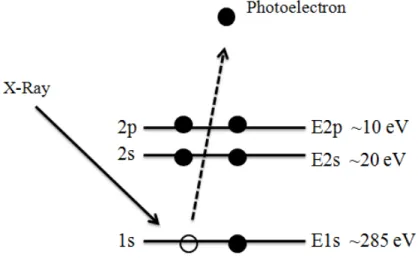
Photoelectric effect was first discovered by Heinrich Rudolf Hertz in 1887. The photoelectric effect is than explained by Albert Einstein in 1905. When a photon hits the surface of the material, it could eject an electron from the surface atoms. The ejected electrons by photons are called photoelectrons. Figure 2.1. shows schematic representation of carbon 1s photoelectron emission process.
Figure 2.1. Schematic illustration of Carbon 1s photoemission process Electrons are bounded to atoms with an energy called binding energy. By measuring the kinetic energy of the photoelectron, it is possible to calculate binding energy of the electron. X-Ray Photoelectron Spectroscopy measures the kinetic energies of the ejected photoelectrons to find the binding energies.
CHAPTER 2 X-RAY PHOTOELECTRON SPECTROSCOPY
2.2. Instrumentation
Kai Siegbahn builds the first commercial X-Ray Photoelectron Spectroscope at 1969 in corporation with Hewlett-Packard. X-Ray Photoelectron Spectroscopy (XPS) also known as Electron Spectroscopy for Chemical Analysis (ESCA) is a spectroscopic technique that measures the electron binding energies of the surface atoms. Binding energies of the electrons are characteristic for each element. The binding energy of the electron gives us information especially about atomic composition and chemical state.
The technique measures the kinetic energies of the ejected photoelectrons. The energy of the valance electrons depends on several variables, therefore we have to measure the energy of the core electrons to successfully characterize the sample. The required photon energy is high to eject core electrons. Therefore X-Rays are used as electromagnetic radiation. The binding energy of the photoelectron is calculated by the formula,
Where is Binding energy of the electron, is the energy photons that is used and is the work function of the instrument. The work function is experimentally found by using standart calibration samples. As the formula above, depends on , so the X-Ray source must be monochromated. The photoelectrons are collected by magnetic lenses to a electron energy analyzer. Electron energy analyzer separates the electrons with respect to their kinetic energy. An electron detector counts the electrons that are separated by electron energy analyzer. The system works under ultra high vacuum because collisions between the electrons and gas
CHAPTER 2 X-RAY PHOTOELECTRON SPECTROSCOPY
5
atoms could both change the energy and decrease the collection efficiency of the electrons. Figure 2.2. shows the general structure of an X-Ray Photoelectron Spectrometer.
Figure 2.2. Schematic illustration of a common X-Ray Photoelectron Spectrometer system.
The spot size of the experiment could be millimeters but the analysis dept is not more than 10 nm. Most commonly used X-Ray sources are Aluminum Kα (1486,6 eV) and Magnesium Kα (1253,6 eV).
List of basic XPS components
-High vacuum chamber -X-Ray source -Sample stage -Electron collection lenses -Electron energy analyzer -Electron counter
CHAPTER 3 EFFECT OF PHOTOVOLTAGE AND
PHOTOCONDUCTIVITY ON BINDING ENERGY SPECTRUM
Chapter 3
Effect of Photovoltage and
Photoconductivity on binding energy
spectrum
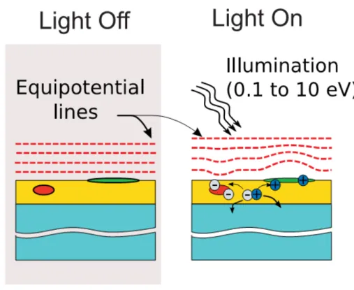
The X-Rays eject electrons from surface atoms of the sample that causes a positive charge. If the material is not a conductor, the material remains charged. Excess positive charge increases the binding energy of electrons and shift the photoelectron spectrum to higher energies. Charging problem limits characterization of non-conducting samples. To overcome charging problem a attachment called flood gun is developed. Flood gun is basically an electron gun used to neutralize the non-conducting samples. In the case of semiconductors, the conductivity changes with optical excitation. Semiconductors respond to light basically depending on the doping level and band gap.
The general behavior of change in surface potentials due to photoconductive and photovoltaic effects are schematically summarized in Figure 3.1. and Figure 3.2.
CHAPTER 3 EFFECT OF PHOTOVOLTAGE AND
PHOTOCONDUCTIVITY ON BINDING ENERGY SPECTRUM
7
Figure 3.1. Surface potentials can shift due to X-ray or flood-gun induced charging.
When light is absorbed by nanoscale semiconducting domains, generated carriers diffuse and drift due to internal electric fields. Carriers may accumulate in different regions of nanostructures or escape to the substrate. Variations in surface state densities, material composition, or doping may be responsible for the creation of nanoscale junctions displaying photovoltaic effects. Photoinduced potential differences between the ground plane and surface domains can arise, as schematically shown in Figure 3.2.
CHAPTER 3 EFFECT OF PHOTOVOLTAGE AND
PHOTOCONDUCTIVITY ON BINDING ENERGY SPECTRUM
Figure 3.2. Surface potential distribution of a composite surface containing n and/or p-type domains can be perturbed upon illumination by light (0.110 eV photons) due to the photovoltaic effect.
If the domain has a p-type top surface (vacuum interface), the binding energies on the surface tend to shift toward positive energies. If the domain has an n-type top surface, the shift is toward negative binding energies (Figure 3.3.).
CHAPTER 3 EFFECT OF PHOTOVOLTAGE AND
PHOTOCONDUCTIVITY ON BINDING ENERGY SPECTRUM
8
Figure 3.3. Resulting potential shifts can be observed in the XPS spectra. A pn junction is characterized by a shift of the surface potential to positive binding energies and an np junction causes a negative shift.
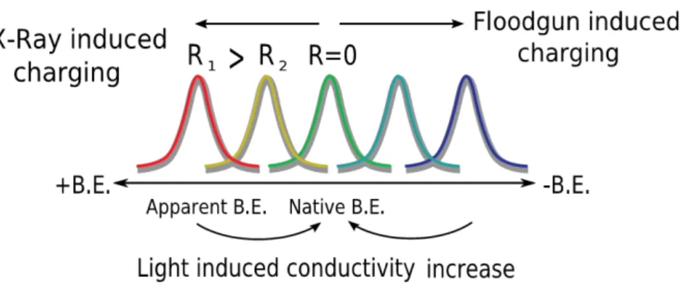
X-ray or external electron-injection related charging results in local variations of surface potentials. [6] If the surface has finite conductivity, X-rays cause a positive charge build-up and the surface potential shifts toward positive energies (Figure 3.4.).
Figure 3.4. Excess positive charge due to X-ray illumination causes a positive shift, and excess negative charge due to electron injection by the flood-gun causes a negative shift. The shifts are proportional to the resistance between the surface and ground. Upon illumination, resistance is reduced and peaks return to the uncharged (native) binding energy.
CHAPTER 3 EFFECT OF PHOTOVOLTAGE AND
PHOTOCONDUCTIVITY ON BINDING ENERGY SPECTRUM
In the presence of an electron flood-gun, the surface charge is compensated by externally injected electrons. If more electrons are injected than lost by photoelectron emission, the surface may be negatively charged and the spectra displays a shift toward negative binding energies. If the conductivity of the surface layer is increased by application of an external light source (photoconductive effect), the charge build-up is decreased due to compensation by available carriers. Photoconductivity causes the peaks to return closer to the native binding energy for both positively and negatively charged surfaces (Figure 3.4.). In an arbitrarily complex composite film, different regions of the film may display both photoconductive and photovoltaic effects. The mechanisms shown in Figure 3.3. and Figure 3.4. may be acting in series or parallel combinations. Simple lumped circuit models as shown in Figure 3.5. and Figure 3.6. can be used to study the dynamic behavior due to photovoltaic and photoconductive effects.
Figure 3.5. A simplified lumped circuit model including a single junction can be used to describe static and dynamic behavior of the surface photovoltaic effect.
CHAPTER 3 EFFECT OF PHOTOVOLTAGE AND
PHOTOCONDUCTIVITY ON BINDING ENERGY SPECTRUM
11
Figure 3.6. A simplified lumped circuit model can be used to describe the time dependent surface potential due to static or dynamic photoconductivity.
Simplified models include a single photovoltaic junction or a light-controlled resistance. The circuits are driven by the photocurrents generated in the junction as well as by external currents due to X-ray illumination and electron injection by the flood gun. The models for photovoltaic and photoconductive cases can be combined in series or parallel cascades, if both effects are simultaneously present. A feature common to all cases is the external current source. The external surface current can be expressed as the sum of the escaping photoelectron current (a constant, proportional to the X-ray photon flux intensity) and the flood gun current , . The flood-gun current can be approximated by
, 1 tanh /2 where is the surface voltage, is the flood-gun bias, is a constant offset, is the maximum electron current achievable from
CHAPTER 3 EFFECT OF PHOTOVOLTAGE AND
PHOTOCONDUCTIVITY ON BINDING ENERGY SPECTRUM
the flood gun and is an experimental parameter. This general form of the , is chosen so that the basic physical mechanism of electron charging of surfaces are included in the model with few adjustable parameters. Electron injection by the flood-gun is dependent on the surface potential, and there are few different characteristic regimes. If the surface potential becomes negative, the flood-gun electrons are repelled from the surface causing a decrease of current. If the surface potential becomes positive, electron capture rate increases. There is a range of positive surface potentials where the electron current is linearly proportional to the surface potential. Owing to the finite availability of electrons, above a certain positive surface voltage, electron current does not further increase and reaches a saturation value .
CHAPTER 4 EXPERIMENTS 13
Chapter 4
Experiments
4.1. Photovoltage
4.1.1 Surface Photovoltage
It is known that light-induced carrier generation and diffusion may disturb the surface pinning and can cause band bending in semiconductors. Therefore, bare semiconductor surfaces may show some degree of surface photovoltaic (SPV) effect.
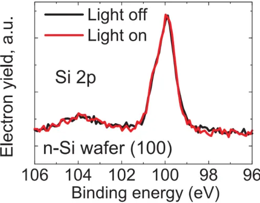
The magnitude and sign of the surface photovoltaic effect depend on many parameters, such as the distribution of surface density of states, the bulk Fermi level position, and mobilities. Such SPV effects can be observed using the XPS, as is demonstrated in Figure 4.1. and Figure 4.2. Since silicon substrates are used in the experiments involving nanoparticles, we first characterize the SPV of the substrates. When an n-type silicon surface (nominal resistivity 110 Ohm-cm) is illuminated with white light, there is no identifiable shift Figure 4.1.
CHAPTER 4 EXPERIMENTS
Figure 4.1. Surface potential of a bare silicon surface is not significantly affected by illumination for an n-type substrate
However, when a p-type silicon surface (resistivity 110 Ohm-cm) is illuminated with white light, a surface potential shift of 0.13 eV is observed (Figure 4.2).
CHAPTER 4 EXPERIMENTS
15
Figure 4.2. Surface potential of a bare silicon surface is significantly affected by illumination for a shift of 0.13 eV is observed for a p-type substrate.
Such shifts have been previously characterized as a function of doping density and type. It is known that p-type silicon produces a greater shift for a given doping level. [14] A greater doping level is known to reduce the SPV. Our observation is in agreement with the previous studies, if it is assumed that the actual doping level of the n-type substrate is higher than p-type.
CHAPTER 4 EXPERIMENTS
4.1.2 Solar cell experiments
4.1.2.1 Fabrication of the solar cell
The surface photovoltaic effects were observed on shallow pn and np junctions. The np junction was a commercial silicon photodiode produced by POCl3 based diffusion. The pn junction was made
in-house by metal induced crystallization. The device studied in the experiments were fabricated by depositing a nominally 400 nm thick amorphous silicon (a-Si) layer onto a hydrofluoric acid (HF) cleaned n-type silicon wafer (110 Ohm cm nominal resistance) using plasma enhanced chemical vapor deposition (using SiH4 as the silicon source, at 250 °C). The a-Si layer was then partially crystallized by thermal evaporation of a thin (50 nm mass thickness) Al layer and annealing in a N2 atmosphere at 500 °C for 30 min. Partial aluminum induced crystallization (ALIC) occurs around hot spots on the surface, and unreacted aluminum was cleaned using HF.
CHAPTER 4 EXPERIMENTS
16
Figure 4.3. Fabrication steps of the ALIC solar cell
A-Si and Aluminum coating
Heat Treatment
Cross section After heat treatment
Photolitography and aluminum evaporation
CHAPTER 4 EXPERIMENTS
Contact pads for the p-type (aluminum, front) and n-type (gold, back) regions were fabricated using lithography and thermal evaporation. The contacts were not further annealed. Aluminum also dopes the crystallized silicon causing formation of p-type domains. [49]
4.1.2.2. Characterization of the solar cell
It was observed that in our process, aluminum silicide/oxide inclusions are formed near the surface as observed by electron microscopy XPS and EDS analysis (Figure 4.4.).
Figure 4.4. EDS map of the fabricated solar cell.
The resulting device performs as a solar cell with a relatively low fill-factor and efficiency (efficiency = 6.4% obtained by comparing to a monocrystalline reference cell of known efficiency, data not shown) with an open circuit voltage of 0.55 V and short circuit current of 6.5 mA/cm2 (Figure 4.5.).
CHAPTER 4 EXPERIMENTS
19
Figure 4.5. I-V curve of the fabricated solar cell
The series and shunt resistances are estimated to be 52 Ω and 850 Ω for a 1.5 cm2 device.
Several analytical methods were used to characterize the structure of the device, including cross-sectional scanning electron microscopy (Figure 4.6.),
CHA Figu EDS HAPTER 4 E ure 4.6. SEM S analysis, a EXPERIME M image of and confoca ENTS f the fabrica al Raman m ated solar ce microscopy ( ell cross-sec (Figure 4.7. ction. .).
CHAPTER 4 EXPERIMENTS
21
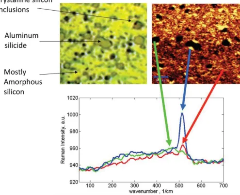
Figure 4.7. Confocal Raman Microscopy image of the fabricated solar cell.
It was observed that aluminum rich inclusions are present on the surface with sizes ranging from 50 to 400 nm vertically and from 50 nm to few micrometers in the sample plane (Figure 4.8.).
CHA Figu sola It w arou effe defe HAPTER 4 E ure 4.8. Sc ar cell. was observe
und the incl ects: fast re ects and d EXPERIME canning ele d in the Ra lusions. The ecombinatio due to defe ENTS ectron micr aman spectr e shunt resi on inside th fects introdu roscopy ima ra that a-Si istance he polycryst uced by a ages of the is partially can be due tal layer du aluminum, e fabricated crystallized e to multiple ue to native as well as d d e e s
CHAPTER 4 EXPERIMENTS
23
nanoscale shorts due to the presence of large AlSi inclusions that run between the top of the p-type surface and the n-type substrate.
4.1.2.3. XPS experiments
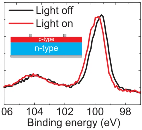
To unambiguously demonstrate photovoltaic effects, ideal pn and np junctions are studied. Two silicon solar cells were studied. The photovoltaic effect can be observed as shown in Figure 4.9. and Figure 4.10. on both np and pn junctions.
Figure 4.9. When np junctions are illuminated, apparent binding energy shifts by VOC are observed. The sign of the shift is negative for
the np junctions
The Si 2p peak in the XPS spectra of an np junction (top side n, bulk of the substrate p-type) from a commercial monocrystalline solar cell is shown to shift toward negative binding energies (Figure 4.7.).
CHAPTER 4 EXPERIMENTS
Figure 4.10. When fabricated pn junctions are illuminated; apparent binding energy shifts by VOC are observed. The sign of the shift is positive for the pn junction.
The shift direction is reversed for the pn junction (top side p-type, bulk of the substrate n-type) (Figure 4.10.). The magnitude of the shift can be estimated using the model in Figure X. The shunting resistance RSH in the model may be an internal resistance, or may be due to grounding of the top surface by an external resistance. In our XPS system, the samples are mounted using insulating clamps or bronze clamps, which act as resistive grounding paths. The effect of the extra ground path is observed in the surface potential for an np silicon junction (Figure 4.12.).
CHAPTER 4 EXPERIMENTS
25
Figure 4.11. Schematic illustration of position dependent XPS experiment.
CHAPTER 4 EXPERIMENTS
As the spectra is collected close to a grounded metal contact, surface potential shifts are decreased. As we move further away from the grounded contact, the surface potential shift increases to negative values (Figure 4.12). The deviation of the surface potential from linear can be understood using a distributed circuit model. We can divide the photovoltaic cell into smaller cells connected to each other by small series resistances. Because of the nonlinear IV characteristics of individual cells, we observe an abrupt shift of the surface potential. The location of the abrupt change depends on the ratio of cell currents and circuit resistances. The XPS data is a result of the convolution of the spot-size of the spectrometer and spatial variations of the surface potential. This causes smoothing of the voltage profile.
4.2. Photoconductivity
4.2.1. Synthesis of CdS nanoparticles
CdS nanoparticles were synthesized by a solvothermal process. [50] Cadmium sulfide nanoparticles with average diameter of 60 nm were prepared by mixing cadmium acetate (Cd(CH3CO2)2), thiourea in ethylene glycol with a molar ratio of 1/8. Figure 4.11. shows the synthesis route.
CHAPTER 4 EXPERIMENTS
27
Figure 4.13. Synthesis route of CdS nanoparticles.
The mixture was heated for1hat180 °C. After cooling, the CdS nano-particles precipitated. The nano-particles were separated from the solvent by centrifugation. The particles were washed three times with ethanol. Substrates were prepared by simple dip coating with ethanol suspended CdS nanoparticles solution and then dried at 100 °C.
CHAPTER 4 EXPERIMENTS
4.2.2. Characterization of CdS nanoparticles
CHAPTER 4 EXPERIMENTS
29
Figure 4.15. SAXS measurements of CdS nanoparticles.
CHA Figu SEM nan that show
4.2
To stud a gr con HAPTER 4 E ure 4.17. XR M and SAX noparticles i t the particl wed the par.3 XPS ex
demonstrat died on a va rounded Au nditions as sh EXPERIME RD results o XS measure is around 6 les are com rticles are nxperiment
te photoco ariety of sub u/Pd surfac hown in Fig ENTS of CdS nano ements show 0 nm. EDS mposed of C anocrystallits
onductive e bstrates. XP e were reco gure 4.18. oparticles. wed that th S measurem Cd and S an ine CdS. effects, CdS PS spectra o orded unde he diameter ments provid nd XRD me S nano-par of CdS part r dark and of the CdS de evidence easurements rticles were ticle film on illuminated S e s e n dCHAPTER 4 EXPERIMENTS
31
Figure 4.18. Photoresponse of CdS nanoparticles on a grounded AuPd surface
Here the flood-gun is turned off, and all charging is due to X-ray induced charging. In the spectra, two distinct peaks are identifiable in the Cd 3d spectrum. In the dark, X-ray charging is seen to cause a shift of one of the peaks toward positive binding energies (408.15 eV for Cd). As the sample is flooded with white light from a superbright LED, this peak shifts toward the native binding energy of Cd in CdS. The smaller peak in the spectrum, originally at 405.4 eV shifts only 0.1 eV to 405.33, which is very close to the original position of cadmium peak for CdS. [20] We attribute this peak to the particles that are directly in contact with the surface (regions with monolayer or submonolayer coverage). The charging effect due to the flood-gun electrons is also shown in Figure 4.19.
CHAPTER 4 EXPERIMENTS
Figure 4.19. Photoresponse of CdS nanoparticles on n-type silicon (experimental data, left), where X-ray charging is dominant ( 0) and electron charging is dominant ( 4 ) in the dark. In both cases, illumination causes reduction of charging. The peaks tend to shift toward the native binding energy (schematic description, right). XPS spectra of a CdS nanoparticle film on a n-doped silicon substrate is recorded under dark and illuminated conditions. The flood-gun voltage was set to 0 and 4 V. The convention for the sign of the flood-gun voltage is equipment dependent. In our case a positive causes increased electron charging. Under dark conditions and = 0 V, a positive shift is observed. The positive shift is a result of X-ray related charging. For = 0, electron charging becomes dominant, and a negative shift of the Cd peak is observed. As the sample is illuminated, both positive and negative shifts decrease. The peaks return closer to the native binding energy. This is attributed to the increase in the conductivity of the CdS film.
CHAPTER 4 EXPERIMENTS
33
4.3. Combined Photovoltage and Photoconductivity
A more general case is the simultaneous presence of both photoconductivity and photovoltaic effects. Band alignment and photovoltaic effects of CdS / p-Si heterojunctions has been previously studied. [21,22] In general photoconductive effect results in a decrease of the charging related shifts and photovoltaic effects cause an increase in the magnitude of shifts. However, with multiple unknowns about a specific sample, it is not possible to separate the two effects without the addition of a swept parameter. The flood-gun potential can be used for this purpose. The surface potential shifts as the flood-gun bias is changed from 0 to 4 V, inducing controlled hole or electron charging. Illumination reduces the resistance, and magnitudes of positive and negative shifts are both reduced. When the peak positions are plotted versus flood-gun potential, if the photovoltaic effect is not present, the curves for dark and illuminated conditions show a crossing-over behavior. This is because there exists a flood-gun potential , for which the X-ray induced current is canceled by electron injection. At this flood-gun voltage, charging is zero regardless of the sample resistance Rs, causing the dark/light curves to cross. If a photovoltaic effect is present, the curves may not cross owing to the shift caused by the photovoltage. The crossing-over or non-crossing over behavior depends on the relative strengths of the photovoltaic and photoconductive effects. The sign of the photovoltage is also a factor in the determination of the crossing/anti-crossing behavior. We demonstrate these effects using samples that show both photoconductivity and photovoltaic effects are present. We measure the XPS spectra of films of CdS nanoparticles on n- and p-type silicon as a function of (Figure 4.20.).
CHAPTER 4 EXPERIMENTS
Figure 4.20. Light-induced changes in the XPS spectra of Cd from CdS nanoparticles on n- and p-type silicon substrates as a function of the flood-gun potential.
CHAPTER 4 EXPERIMENTS
35
Figure 4.21. Peak positions are plotted for dark and illuminated cases of CdS/p-Si.
Figure 4.22. Peak positions are plotted for dark and illuminated cases of CdS/n-Si.
CHAPTER 4 EXPERIMENTS
CdS forms an np junction on p-type silicon and displays both photovoltaic and photoconductive effects. CdS films on an n-type silicon substrate show photoconductivity dominantly. For n-type silicon, a crossing of the peak energies is observed under dark and illuminated conditions. The experimental data in Figure 4.21 and 4.22 can be qualitatively reproduced assuming the presence of a photoconductive effect Figure 4.23 and Figure 4.24..
Figure 4.23. Theoretical model can be used to predict behavior for the n-type CdS on p-type silicon. The change from crossing to noncrossing curves are attributed to the presence of a photovoltaic effect for the n-CdS/p-Si case. The anticrossing behavior is not universal but is dependent on experimental and sample related parameters such as the total induced photovoltage at the junction, floodgun and X-ray induced surface currents, and strength of the photoconductivity effect.
CHAPTER 4 EXPERIMENTS
37
Figure 4.24. Theoretical model can be used to predict behavior for the n-type CdS on n-silicon.
This observation suggests the absence of a strong photovoltaic effect between the n-type CdS film and n-type Si. For CdS on p-type silicon, the photoconductivity of the nanoparticle film is accompanied by the photovoltaic effect between the CdS/p-type silicon. The wavelength dependence of the effects can be seen in Figure 4.25..
CHAPTER 4 EXPERIMENTS
Figure 4.25. Photoconductive and photovoltaic effects are also shown to be wavelength dependent: When illuminated by 532 nm light (above the CdS bandgap), both CdS and silicon display light-induced effects, silicon showing only surface photovoltaic effect and CdS displaying both photovoltaic and photoconductive effects. When illuminated by a 650 nm laser, the sample absorbs light only in the p-type silicon substrate producing shifts equal to the silicon surface photovoltage shown in Figure X. In this case, the apparent CdS binding energy follows the potential of the silicon substrate it rests upon.
The CdS film on a p-type silicon substrate is illuminated with 532 (2 mW nominal power) and 650 nm (1 mW nominal power) lasers. CdS nano-particles have a bandgap above 2.42 eV, [23] therefore no absorption is expected for 650 nm illumination in the CdS layer. Here, the flood-gun is turned off and all charging is due to X-ray exposure. The CdS layer remains charged under 650 nm illumination. However, p-type silicon shows a shift of 0.13 eV (as was previously observed on a bare p-type sample, shown in Figure X). Since the CdS film is referenced to the silicon surface, the apparent binding energy of Cd3d is also shifted by 0.13 eV. When the sample is illuminated using 532
CHAPTER 4 EXPERIMENTS
39
nm laser, both CdS and Si display photoactivity, Cd3d shifting as much as 2.5 eV. The photoconductivity related shift of the Cd3d line on an n-type substrate is about 2.1 eV, with no significant shift of the Si peak. We therefore conclude that the CdS/p-Si junction displays a photovoltage of about 0.27 eV. For CdS/p-type silicon, there are two photovoltaic junctions (CdS/p-Si and p-Si surface) and a single photoconductive region (CdS), all acting in series. Wavelength dependent measurement allows us to distinguish shifts due to individual junctions.
4.4. Dynamic Characterization of pn junction solar cell
Previously dynamic characterization of surface voltage distributions were carried out using externally modulated sample bias. A simplified RC model of a composite surface was shown to quantitatively predict XPS spectra. The convolution approach used for simulation of XPS spectra under dynamic excitation [24] can be extended to include the photoeffects using the model shown in Figure X. A pn junction (ALIC cell) is placed inside the XPS chamber and subjected to static and modulated illumination by an external laser (650 nm, multimode diode laser, 0.5 mW) with modulation frequencies ranging from 0.1 Hz to 1 MHz, while the photoelectron spectra are collected. The surface potentials of various domains on the device are modulated according to their local electronic properties. The electronic properties determine the equivalent lumped circuit elements such as capacitances, shunt, and series resistances. We demonstrate the applicability of the technique on a pn junction known to display the photovoltaic effect dominantly. We use the model in Figure X in a circuit simulator to calculate the dynamic response of the lumped circuit. The time-dependent surface potentials are calculated with the simulator, then the line shape
CHAPTER 4 EXPERIMENTS
functions are calculated using a histogram of the time-series of the surface voltage. The lineshapes are then used to estimate the peak position shifts and broadenings as described elsewhere. [25] It is seen that, if the frequency of modulation is slow compared to the characteristic cutoff frequency of the surface response, the line shape function resembles a double delta function separated by (Figure 4.26.).
Figure 4.26. Surface voltages under modulated illumination are calculated using the simplified circuit model. Time varying surface potentials are used to calculate line shape function using a histogram. The line shape function is then convoluted with the original unmodulated XPS data to predict spectra under modulated illumination.
CHAPTER 4 EXPERIMENTS
41
The resulting convolved peak shape has a greater width and reduced peak intensity. The peak position is shifted to about /2. As the modulation frequency is increased above the cutoff frequency of the junction, the junction acts like a low-pass filter. In this case, the line shape becomes like a single delta function. The width of the observed peak becomes narrower, closer to the native width of the peak. This is accompanied by a slight shift of the peak position toward Simulation results for the ALIC cell, using parameters extracted from dark and illuminated IV curves are shown in Figure 4.27.. The model predicts the correct form of frequency dependence.
Figure 4.27. Apparent binding energy and full-width-at-half-maximum of the oxygen peak on a pn ALIC cell as a function of modulation frequency is shown.
CHAPTER 4 EXPERIMENTS
It is seen that when model parameters obtained by conventional device characterization methods are used, theoretical calculation of the peak shifts and broadening agree with the XPS measurements. This observation suggests that model parameters of solar cells can be extracted through numerical analysis and using XPS measurements only. In principle, correlations of optoelectronic properties can be established between different peaks automatically. Similar correlations of electronic properties were extracted using modulated external bias. [24,26] Location dependent dynamic characterization is also possible. Changes in the SPV frequency response can be observed if the response is measured close to or away from the contacts (Figure 4.28.)
Figure 4.28. The frequency dependence of apparent binding energies of residual aluminum, collected at points close to and away from the contact, is shown. Slightly different frequency responses are observed. The photoconductivity can be studied dynamically as well as through photovoltaic effects. We use pulsed illumination on a CdS nanoparticle
CHAPTER 4 EXPERIMENTS
43
film on an n-type substrate. Light pulses of duration 5 ms with a repetition rate is incident on the sample. A superbright white LED is used as the light source. The flood gun is turned off and only X-ray gun charging is present. During the light pulse, photoconductivity reduces the resistance of the film ( 0). In this period, the surface may be thought as shorted to ground. During the dark period, the surface behaves like an RC circuit (
30 MΩ, C ≈ 0,2 nF), charged by the X-ray current (Ix = 100 nA). The
circuit element values are obtained by fitting. If the pulse repetition rate is increased, the film spends more time in the short state. Therefore, at low frequencies the film is mostly charged and at high frequencies the film is mostly shorted. The gradual transition between fully off and fully on states can be observed in the XPS data (Figure 4.29.).
CHAPTER 4 EXPERIMENTS
Figure 4.29. The effect of pulsed illumination on the Cd3d peak for a CdS nanoparticle film on n-type silicon. Because of modulation of CdS film conductivity by a 5ms long light pulse of varying repetition frequency, the charging is intermittently reduced. The flood-gun is turned off and X-ray related positive charging is present only. The peak position shifts as a function of repetition frequency frep.
When the pulse frequency is close to the effective RC time constant of the film, maximal peak broadening occurs. This feature, theoretically estimated by the model, can be observed in the experimental results shown in Figure 4.30..
CHAPTER 4 EXPERIMENTS
45
Figure 4.30. Broadening of the peak is observed when pulse-to-pulse separation time is near the effective RC time constant of the film. Experimental observations can be understood using the model given in Figure X. R and C values, as well as the X-ray induced current Ix are
fitting parameters. Satellite graphs show theoretically calculated transient surface potentials for slow and fast pulse repetition rates.
4.5. CNT-Si heterojunction
4.5.1. Sample Preparation and characterization
The MWCNTs are commercially obtained and are around 50 nm in width and 1015 m in length (Figure 4.31.).
CHAPTER 4 EXPERIMENTS
Figure 4.31. SEM image of MWCNTs.
MWCNTs were dissolved in dichloromethane (DCM) and sonicated for 1 h. A similar procedure was used for SWCNTs (Figure 4.32.).
CHAPTER 4 EXPERIMENTS
47
Figure 4.32. SEM of SWCNTs.
After sonication the substrates were prepared by dip coating with SWCNTs & DCM or MWCNTs & DCM solution than dried at 100 °C.
4.5.2. XPS Experiments
We apply the technique to the characterization of light induced changes in the XPS spectra of single and multiwall carbon nanotubes (SWCNT and MWCNT) on metal and semiconductor substrates. Electronic structure and properties of SWCNTs and MWCNTs have been extensively studied both theoretically and experimentally. [27,33] Also CNTs have found application in photovoltaic devices both as contacts and active layers. [34-40] For the sake of simplicity, the experiments were performed without activating the flood-gun. In this case, all charging must be due to X-ray related charging. It is observed
CHAPTER 4 EXPERIMENTS
that the carbon peak from a thin film of MWCNTs on a n-type silicon surface demonstrates a shift of 0.3 eV upon illumination (Figure 4.33.)
Figure 4.33. light-induced shifts can be observed in the carbon spectrum with a multiwall carbon nanotube film on an n-type substrate No significant shifts are observed on p-type silicon or on AuPd-coated substrates(Figure 4.34.).
CHAPTER 4 EXPERIMENTS
49
Figure 4.34. CNTs show no significant shift is observed on a p-type silicon substrate.
A similar shift is observed with a SWCNT film on n-type silicon substrates(Figure 4.35.).
CHAPTER 4 EXPERIMENTS
Figure 4.35. Similar shifts are observed for single-wall nanotubes on an n-type silicon substrate with native oxide.
When the native oxide layer (typically few nm thick) on the substrate is cleaned using HF prior to casting of the CNT film, it is observed that the light induced shift is decreased (Figure 4.36.).
CHAPTER 4 EXPERIMENTS
51
Figure 4.36. Light induced shifts are reduced for CNTs on n-Si after removal of the native oxide with HF.
Since only X-ray charging is possible without the flood-gun, in this case the photoconductive effect may only produce a negative shift, in favor of reducing charging. As the observed light-induced shift is positive, it is due to the photovoltaic effect, the CNT film acting effectively as a p-type domain on an n-type substrate. This conclusion is also supported by observation of the effect only on n-type substrates. To understand the origin of the observed shift, we model the electrostatic problem at the CNT/oxide/silicon interface under illumination using rate equations, taking into account the generation recombination and electron/hole tunneling rates as shown in Figure 4.37..
CHAPTER 4 EXPERIMENTS
Figure 4.37. Schematic description of the band alignment of carbon nanotube film on silicon under external illumination.
We assume carrier generation in the CNT film only. In CNTs, the electron and hole properties are highly symmetric, [28-41] and we may assume a density of states for the CNT ensemble symmetric around the CNT affinity of 4.5 eV. [35,42,43] We assume that the relaxation inside the CNT film is rapid, and the CNT film is in equilibrium, with separate quasi Fermi levels for electrons and holes. We also assume that the escape rates of carriers to the substrate are dominated by direct tunneling rates. Under these simplifying assumptions, the net charge on the CNT film and resulting surface potential is determined by an imbalance between the electron and hole tunneling rates rn and rp.
CHAPTER 4 EXPERIMENTS
53
G and R are related to escape rates and carrier concentration change rates by
∆
∆
where Fox is the barrier (oxide) field. At a given time, the electron and
hole concentrations in the CNT film are ∆n and ∆p, giving a net charge concentration of ∆q = ∆p - ∆n. The barrier field is related to charge on the CNT film by ∆q/2ε . Under steady state conditions,
∆ ∆
∆
∆ 0 ∆ ∆
The surface potential shift, ∆
where tox is the oxide (barrier) thickness. The net charge can be
rewritten as,
∆ ∆ ∆ ∆ 1
The tunneling rates rn and rp are assumed to be determined by direct
tunneling. For small barrier fields (Fox = 0),
exp 3 , 2 Where
4 2 , 3ħ
CHAPTER 4 EXPERIMENTS
, VB,i is the barrier height for tunneling and mox,i is the tunneling
effective mass. [46-48] Hence, tunnel rates are exponentially dependent on the electron and hole barriers (VB,e 4.5 and VB,p 4.66
eV) and barrier thickness tox, electron tunneling being typically faster.
Hence, a positive net charge accumulates on the CNT film and a surface potential shift ∆Vs proportional to the oxide thickness is
expected. As the surface potential shift increases, changing barrier field tends to readjust the electron and hole escape rates and an equilibrium value proportional to the oxide thickness is achieved. The estimations of this model agree with the observations shown in Figure X and Figure X, where a decrease of the surface photovoltage is seen for reduced barrier thickness. The observed photovoltage polarity is in parallel with previous demonstrations of solar-cells made up of carbon-nanotube films on n-type silicon. [39]
CHAPTER 4 CONCLUSION
55
Chapter 5
Conclusion
We present an extended model of surface potentials in an XPS experiment in the presence of photovoltaic and photoconductive effects. The approach is shown to distinguish between surface voltage shifts due to photovoltaic or photoconductive effects. The model also can be used to predict dynamical behavior of surface voltages under modulated illumination. Wavelength dependent absorption and chemically specific response is observed in composite surfaces. The origins of the shifts can be understood by referring to the predictions of the presented model. The method can be used in combination with standard XPS procedures, such as depth profiling and angle resolved XPS, to provide greater insight into the origins of optoelectronic effects. The demonstrations also underline the importance of illumination in an XPS experiment.
CHAPTER 4 BIBLIOGRAPHY
Bibliography
[1] Siegbahn, K.; Hammond, D.; Fellner-Feldegg, H.; Barnett, E. F. Electron Spectroscopy with Monochromatized X-rays. Science 1972, 176, 245–252.
[2] Siegbahn, K. Electron Spectroscopy for Atoms, Molecules, and Condensed Matter. Science 1982, 217, 111–121.
[3] Smith, N. V.; Woodruff, D. P. Surface Spectroscopies with Synchrotron Radiation. Science 1982, 216, 367–372.
[4] Turner, N.; Schreifels, J. Surface Analysis: X-ray Photoelectron Spectroscopy and Auger Electron Spectroscopy. Anal. Chem. 2000, 72, 99R–110R.
[5] Chaudhury, M.; Whitesides, G. Correlation between Surface Free Energy and Surface Constitution. Science 1992, 255, 1230–1232. [6] Lau, W. M. A Surface Charging Technique in Photoemission Spectroscopic Studies of DielectricSemiconductor Structures. J. Appl. Phys. 1990, 67, 1504–1509.
[7] Suzer, S. Differential Charging in X-ray Photoelectron Spectroscopy: A Nuisance or a Useful Tool. Anal. Chem. 2003, 75, 7026–7029.
[8] Karadas, F.; Ertas, G.; Suzer, S. Differential Charging in SiO2/ Si System as Determined by XPS. J. Phys. Chem. B 2004, 109, 1515– 1518.
CHAPTER 4 BIBLIOGRAPHY
57
[9] Demirok, U. K.; Ertas, G.; Suzer, S. Time-Resolved XPS Analysis of the SiO2/Si System in the Millisecond Range. J. Phys. Chem. B 2004, 108, 5179–5181.
[10] Suzer, S.; Sezen, H.; Ertas, G.; Dana, A. XPS Measurements for Probing Dynamics of Charging. J. Electron Spectrosc. Relat. Phenom. 2010, 176, 52–57.
[11] Sezen, H.; Ertas, G.; Dana, A.; Suzer, S. ChargingDischarging of Thin PS/PMMA Films as Probed by Dynamic X-ray Photoelectron Spectroscopy. Macromolecules 2007, 40, 4109–4112.
[12] Filip-Granit, N.; van der Boom, M. E.; Yerushalmi, R.; Scherz, A.; Cohen, H. Submolecular Potential Profiling Across Organic Monolayers. Nano Lett. 2006, 6, 2848–2851.
[13] Cohen, H. Transient Charge Accumulation in a Capacitive Self-Assembled Monolayer. Nano Lett. 2006, 6, 2462–2466.
[14] Clabes, J.; Henzler, M. Determination of Surface States on Si(111) by Surface Photovoltage Spectroscopy. Phys. Rev. B 1980, 21, 625–631.
[15] Bardeen, J. Surface States and Rectification at a Metal Semiconductor Contact. Phys. Rev. 1947, 71, 717–727.
[16] Zeng, T.-W.; Hsu, F.-C.; Tu, Y.-C.; Lin, T.-H.; Su, W.-F. Kelvin Probe Force Microscopy Study on Hybrid P3HT:Titanium Dioxide Nanorod Materials. J. Electron Spectrosc. Relat. Phenom. 2009, 479, 105–108.
[17] Schlaf, R.; Hinogami, R.; Fujitani, M.; Yae, S.; Nakato, Y. Fermi level Pinning on HF Etched Silicon Surfaces Investigated by
CHAPTER 4 BIBLIOGRAPHY
Photoelectron Spectroscopy. J. Vac. Sci. Technol. A 1999, 17, 164– 169.
[18] Cohen, H.; Sarkar, S. K.; Hodes, G. Chemically Resolved Photovoltage Measurements in CdSe Nanoparticle Films. J. Phys. Chem. B 2006, 110, 25508–25513.
[19] Cohen, H. Chemically Resolved Electrical Measurements in Organic Self-Assembled Molecular Layers. J. Electron Spectrosc. Relat. Phenom. 2010, 176, 24–34.
[20] Christian, J., Ed. Handbook of Photoelectron Spectroscopy; Physical Electronics: Eden Prairie, MN, 1992.
[21] Coluzza, C.; Garozzo, M.; Maletta, G.; Margadonna, D.; Tomaciello, R.; Migliorato, P. NCdSPSi Heterojunction Solar-Cells. Appl. Phys. Lett. 1980, 37, 569–572.
[22] Garcia, F.; Ortizconte, A.; Saneto, A. CdS/PSi Solar Cells Made by Serigraphy. Appl. Phys. Lett. 1988, 52, 1261–1263.
[23] Kittel, C. Introduction to Solid State Physics, 7th ed.; Wiley: New York, 1976.
[24] Suzer, S.; Dana, A. X-ray Photoemission for Probing Charging/Discharging Dynamics. J. Phys. Chem. B 2006, 110, 19112– 19115.
[25] Dana, A. Lineshapes, Shifts, and Broadenings in Dynamical X-ray Photoelectron Spectroscopy. Appl. Surf. Sci. 2009, 256, 1289–1295. [26] Suzer, S.; Sezen, H.; Dana, A. Two-Dimensional X-ray Photoelectron Spectroscopy for Composite Surface Analysis. Anal. Chem. 2008, 80, 3931–3936.
CHAPTER 4 BIBLIOGRAPHY
59
[27] Wildoer, J.; Venema, L.; Rinzler, A.; Smalley, R.; Dekker, C. Electronic Structure of Atomically Resolved Carbon Nanotubes. Nature 1998, 391, 59–62.
[28] Chico, L.; Crespi, V.; Benedict, L.; Louie, S.; Cohen, M. Pure Carbon Nanoscale Devices: Nanotube Heterojunctions. Phys. Rev. Lett. 1996, 76, 971–974.
[29] Dekker, C. Carbon Nanotubes as Molecular Quantum Wires. Phys. Today 1999, 52, 22–28.
[30] Zhou, C.; Kong, J.; Yenilmez, E.; Dai, H. Modulated Chemical Doping of Individual Carbon Nanotubes. Science 2000, 290, 1552– 1555.
[31] Derycke, V.; Martel, R.; Appenzeller, J.; Avouris, P. Controlling Doping and Carrier Injection in Carbon Nanotube Transistors. Appl. Phys. Lett. 2002, 80, 2773–2775.
[32] Tans, S.; Verschueren, A.; Dekker, C. Room-Temperature Transistor Based on a Single Carbon Nanotube. Nature 1998, 393, 49– 52.
[33] Li, X.; Zhu, H.; Wei, J.; Wang, K.; Xu, E.; Li, Z.; Wu, D. Determination of Band Gaps of Self-Assembled Carbon Nanotube Films Using Tauc/DavisMott Model. Appl. Phys. A 2009, 97, 341– 344.
[34] Kymakis, E.; Amaratunga, G. Single-Wall Carbon Nanotube/ Conjugated Polymer Photovoltaic Devices. Appl. Phys. Lett. 2002, 80, 112–114.
CHAPTER 4 BIBLIOGRAPHY
[35] Behnam, A.; Johnson, J.; Choi, Y.; Noriega, L.; Ertosun, M. G.; Wu, Z.; Rinzler, A. G.; Kapur, P.; Saraswat, K. C.; Ural, A. MetalSemiconductorMetal Photodetectors Based on Single-Walled Carbon Nanotube FilmOGaAs Schottky Contacts. J. Electron Spectrosc. Relat. Phenom. 2008, 103, 114315.
[36] Behnam, A.; Johnson, J. L.; Choi, Y.; Ertosun, M. G.; Okyay, A. K.; Kapur, P.; Saraswat, K. C.; Ural, A. Experimental Characterization of Single-Walled Carbon Nanotube Film Si Schottky Contacts Using MetalSemiconductorMetal Structures. Appl. Phys. Lett. 2008, 92, 243116.
[37] Behnam, A.; Choi, Y.; Noriega, L.; Wu, Z.; Kravchenko, I.; Rinzler, A. G.; Ural, A. Nanolithographic Patterning of Transparent, Conductive Single-Walled Carbon Nanotube Films by Inductively Coupled Plasma Reactive Ion Etching. J. Vac. Sci. Technol., B 2007, 25, 348–354.
[38] Tzolov, M. B.; Kuo, T.-F.; Straus, D. A.; Yin, A.; Xu, J. Carbon NanotubeSilicon Heterojunction Arrays and Infrared Photocurrent Responses. J. Phys. Chem. C 2007, 111, 5800– 5804.
[39] Wei, J.; Jia, Y.; Shu, Q.; Gu, Z.; Wang, K.; Zhuang, D.; Zhang, G.; Wang, Z.; Luo, J.; Cao, A.; et al. Double-Walled Carbon Nanotube Solar Cells. Nano Lett. 2007, 7, 2317–2321.
[40] Jia, Y.; Wei, J.; Wang, K.; Cao, A.; Shu, Q.; Gui, X.; Zhu, Y.; Zhuang, D.; Zhang, G.; Ma, B.; et al. NanotubeSilicon Heterojunction Solar Cells. Adv. Mater. 2008, 20, 4594–4598.
CHAPTER 4 BIBLIOGRAPHY
61
[41] Jarillo-Herrero, P.; Sapmaz, S.; Dekker, C.; Kouwenhoven, L.; van der Zant, H. Electron-Hole Symmetry in a Semiconducting Carbon Nanotube Quantum Dot. Nature 2004, 429, 389–392.
[42] Ago, H.; Kugler, T.; Cacialli, F.; Salaneck, W.; Shaffer, M.; Windle, A.; Friend, R. Work Functions and Surface Functional Groups of Multiwall Carbon Nanotubes. J. Phys. Chem. B 1999, 103, 8116– 8121.
[43] Shiraishi, M.; Ata, M. Work Function of Carbon Nanotubes. Carbon 2001, 39, 1913–1917.
[44] Sarkar, S. K.; Hodes, G.; Kronik, L.; Cohen, H. Defect-Dominated Charge Transport in Si-Supported CdSe Nanoparticle Films. J. Phys. Chem. C 2008, 112, 6564–6570.
[45] Akca, I. B.; Dana, A.; Aydinli, A.; Turan, R. Comparison of Electron and Hole Charge-Discharge Dynamics in Germanium Nanocrystal Flash Memories. Appl. Phys. Lett. 2008, 92, 052103.
[46] Brar, B.; Wilk, G.; Seabaugh, A. Direct Extraction of the Electron Tunneling Effective Mass in Ultrathin SiO2. Appl. Phys. Lett. 1996, 69, 2728–2730.
[47] Stadele, M.; Sacconi, F.; Di Carlo, A.; Lugli, P. Enhancement of the Effective Tunnel Mass in Ultrathin Silicon Dioxide Layers. J. Appl. Phys. 2003, 93, 2681–2690.
[48] Schenk, A.; Heiser, G. Modeling and Simulation of Tunneling Through Ultra-Thin Gate Dielectrics. J. Appl. Phys. 1997, 81, 7900– 7908.
CHAPTER 4 BIBLIOGRAPHY
[49] Nast, O.; Brehme, S.; Pritchard, S.; Aberle, A. G.; Wenham, S. R. Aluminium-Induced Crystallisation of Silicon on Glass for Thin-Film Solar Cells. Sol. Energy Mater. Sol. Cells 2001, 65, 385–392.
[50] Feldmann, C.; Metzmacher, C. Polyol Mediated Synthesis of Nanoscale MS Particles (M = Zn, Cd, Hg). J. Mater. Chem. 2001, 11, 2603–2606
[51] Ekiz, O.O.;Mizrak K.;Dana, A. Chemically Specific Dynamic Characterization of Photovoltaic and Photoconductivity Effects of Surface Nanostructures. ACS Nano, 2010, 4 (4), pp 1851–1860.