Investigation of optical and device parameters of colloidal copper
tungsten selenide ternary nanosheets
Murat Yıldırım1 · Adem Sarılmaz2 · Faruk Özel2
Received: 15 July 2017 / Accepted: 3 October 2017 / Published online: 10 October 2017 © Springer Science+Business Media, LLC 2017
1 Introduction
Recently, scientists have focused on renewable energy sources to supply the increased energy demand. Semicon-ductors are prominent in renewable energy studies, espe-cially ternary compound materials have been the center of attraction because of their as narrow band-gap, high photo-catalytic, ferromagnetism, antiferromagnetism and non-lin-ear optical activity features [1]. Copper based nanoparticles have gained particular interest in electronic applications due to their unique optical and electrical properties. Copper chal-cogenide nanoparticles are p-type semiconductors and are widely used to make heterojunctions in solar cell devices [2,
3]. Copper selenide nanoparticles are mostly found as CuSe, Cu2Se and Cu3Se2 with their bulk materials possessing band gap energy between 1 and 2.3 eV [4, 5]. Various results have been reported for the synthesis of CuxMSe4 (M = Sb [6, 7],
P [8], Sn [9], Cr [10, 11], As [12]) nanoparticles. These methods resulted in various shaped and sized particles. Kalenga et al. [2] have reported on the synthesis of copper selenide using a microwave assisted synthesis route. They have explored the microwave-assisted method with the aim of producing high quality nanoparticles. There a few reports on crystal structure, optical and electrical feature of Cu2XY4
(X: Mo or W; Y: S or Se) which ones of ternary compound materials, in literature [13–23]. Crossland et al. [13] have reported that crystal structure change of Cu2AB4 (A = Mo or W; B = Se, S or S/Se) as depending on synthesis tem-perature. According to study of Liang et al. photocatalytic performance is investigated of Cu2MoS4 nanocrystals [14].
Schottky barrier devices involve a metal–semiconduc-tor junction and result in diode behavior. Copper selenide is usually employed in optoelectronic devices as a precur-sor for CIS and CIGS devices. Schottky devices based on binary metal chalcogenide semiconductor nanoparticles have
Abstract Hot injection synthesis route has been
success-fully applied for the preparation of high quality Cu2WSe4 (CWSe) nanosheets in order to determine their optical characterization and device parameters. Several techniques including XRD, SEM, TEM and SAED were used to char-acterize these nanosheets. These techniques confirmed that Cu2WSe4 nanosheets crystal shapes of synthesized are
rectangular and square sheet and the average crystal size is between 20 and 40 nm. The spin coating technique was successfully used to deposit uniform of Cu2WSe4 thin film. Cu2WSe4 thin film has directly transition with a band gap
of 1.64 eV. The dispersion of the refractive index is dis-cussed in terms of the single oscillator Wemple–Didomen-ico (WD) model. The single oscillator energy (E0
) and the dispersion energy (Ed
)
were estimated. Au/Cu2WSe4/n-Si
structures was fabricated and its main electrical characteris-tics described by using current–voltage (I–V) methods. The forward and reverse bias current voltage (I–V) characteristics of Au/Cu2WSe4/n-Si at room temperature were studied to
investigate its basic electrical parameters [i.e. saturation cur-rent (I0), ideality factor (n), barrier height (ΦB), series (Rs)]. Structural and optical mechanisms were discussed for future applications in optoelectronic devices.
* Murat Yıldırım
[email protected] * Faruk Özel
1 Department of Biotechnology, Faculty of Science, Selçuk
University, 42030 Konya, Turkey
2 Department of Metallurgical and Materials Engineering,
Faculty of Engineering, Karamanoğlu Mehmetbey University, 70200 Karaman, Turkey
been reported and largely involve PbS or PbSe nanoparti-cles. These devices that reported poor performances due to their instability in air and have only shown improvement when kept in a glove box. The poor performances have been on occasion attributed to the use of long chained capping ligands. A number of reports have attributed poor device performances due to the poor interface between two materi-als particularly between the metal and semiconductor. Con-sequently different architectures, materials and treatments have been employed to improve the junction [2].
Present research paper deals with the results and discus-sions about crystallographic, morphological, optical proper-ties of Cu2WSe4 nanosheets synthesized via facile hot injec-tion method. Furthermore, we report on a Schottky device based on copper tungsten selenide nanosheets and we study the properties of barrier junction properties.
2 Materials and methods 2.1 Materials
Copper(II) chloride dehydrate (99.999%), tungsten(IV) chloride (95%), selenium powder (99.99%), ethanol (abso-lute, ≥ 99.8%), methanol and acetone were purchased from Sigma-Aldrich. Oleylamine 80–90% (OLA) was supplied from Acros Organic. Oleic acid (OLAC) (≥ 99%) was pur-chased from Fisher Scientific. Toluene (99%) was purpur-chased from VWR. Single crystalline n-type Si wafer was purchased Waferworld Inc.
2.2 Hot injection synthesis of colloidal C2WSe4
nanosheets
Cu2WSe4 nanosheets are synthesized by hot-injection method which is advantageous in terms of synthesis time and temperature, by using metal salts precursors as start-ing materials [13]. This method has a same synthesis pro-cesses with previously published studies [24, 25]. 1 mmol CuCl2·H2O, 0.5 mmol WCl4 and 10 ml OLA are mixed
in a 25 ml three-neck flask and heated to180 °C under Ar flow. 1 ml OLA-Se solution has been injected into reaction medium when solution color changed from blue to green-ish-blue. Later, the temperature of the reaction mixture is increased to 300 °C and kept for 30 min by stirring and then it is reduced to 80 °C and 2 ml oleic acid is added to reaction flask. After that, toluene–ethanol (3:1) mixtures are added and centrifuged to precipitate Cu2WSe4 nanosheets in
2500 rpm for 60 s. Ultimately; Cu2WSe4 nanosheets are left
to dry at 70 °C for 2 h. where after they are washed several times with ethanol.
2.3 Preparation of Cu2WSe4 thin films and device
applications
The optical properties of Cu2WSe4 were determined by
placing the toluene–propanol mixtures and the Cu2WSe4 nanosheets were spin coated onto glass substrate at room temperature. This coating has been stirred for 30 min. In advance of the coating, glass substrate is cleaned within trichloroethylene, methanol and acetone where each step takes for 5 min by using an ultrasonic cleaner. Later it is cleaned with 18 MΩ cm resistivity deionized water and dried in N2 gas. The final cleansing process of glass substrate
is carried out by ultraviolet-generated ozone (UVO) cleaner. As inorganic semiconductors for device application, phosphorus doped n-type Si single crystalline wafer grown by Czochralski method with 300 m thick, (100) surface ori-entation and 20 Ω cm resistivity was used. The CuWSe solu-tion was stirred for 3 min at a magnetic stirrer. The wafer was dipped by using an ultrasonic cleaner for 10 min in boiling trichloroethylene, acetone and ethanol to remove organic contaminants. The Si substrate was chemically cleaned using the RCA cleaning procedure [26]. Then, a low-resistivity ohmic back contact to n-type Si wafer was made by using aluminum (Al), followed by a temperature treatment at 400 °C for 5 min in N2 atmosphere. Al evapo-ration process was carried out in a vacuum coating unit at about 1 × 10⁶ Torr. The native oxide on the front surface
of the wafers was removed in HF:H2O (1:10) solution and
finally was rinsed in 18 MΩ cm resistivity deionized water for 60 s. The CuWSe solution was spin coated on the cleaned the glass substrate and n-type Si wafer with the 1200 rpm spin speed for 60 s with a Laurell Spin Coater. High purity gold (Au, 99.99%) metal contacts with 150 nm thickness were thermally evaporated using a mask with 1.75 mm diameter in a high vacuum coating unit to form the top con-tact onto CuWSe/n-Si film surface, respectively.
2.4 Instrumentation
XRD pattern and TEM results are recorded to analyze phase purity, morphology, crystal structure and size distribution by Bruker D8 XRD and JEOL JEM-2100F TEM respec-tively. The thickness measurement of the coated Cu2WSe4
thin film has been performed by stylus profilometre Veeco Dektak 150 and the thickness has been determined approxi-mately as 190 nm. SEM specimen of the Cu2WSe4 thin film on the glass substrate was coated with gold to increase the conductivity. Scanning Electron Microscope, SEM Model Zeiss Evo® LS 10 with accelerating voltage 30 kV was used
to study the surface morphology of the Cu2WSe4 thin film. UV–VIS–NIR spectroscopy (JASCO model V-670-UV/ VIS/NIR) was used to determine the transmittance, (T), and reflectance, (R), properties of the Cu2WSe4 nanosheets thin
film source. The Schottky junction was characterized by cur-rent (I) and voltage (V) measurements using a digital source meter (Keithley Instruments Inc., Model 2400) in the dark.
3 Results and discussions
3.1 Characterization of Cu2WSe4 nanosheets
Phase purity and crystalline structure of Cu2WSe4
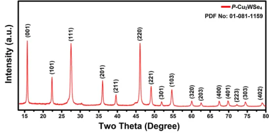
nanosheets were analyzed by XRD diffractometer and these results are given in Fig. 1. As seen in previous studies, there are two main phases of Cu2WSe4 nanosheets which are P-Cu2WSe4 (primitive) and I-Cu2WSe4 (body centered)
[13–25]. In this study, Cu2WSe4 nanosheets were obtained
as P-Cu2WSe4 (primitive) by bonding of each Se atoms to two Cu and one W atom. As can be clearly seen from Fig. 1, Cu2WSe4 nanosheets have pure tetragonal crystal structure.
Intense peaks at 15.7, 22.4, 27.5, 36.0, 39.6, 46.1, 49.1, 52.0, 54.7,60.1, 62.6, 67.5, 69.8, 72.2, 74.5 and 79.0 correspond to planes (001), (101), (111), (201), (211), (220), (221), (301), (103), (320), (203), (400), (401), (223), (303) and (402) respectively and this results compatible with literature (PDF No. 01-081-1159). But XRD peaks of CWSe slightly shifted to lower values than CWS because of diameter of Se atoms is larger than S atoms. The diffraction peaks are broad due to small particle size. Any characteristic peaks of other crystalline forms weren’t detected so we can claim to obtain Cu2WSe4 nanosheets had high purity. Moreover, size distributions of CWSe nanocrystals were measured for each XRD peak by Scherrer’s equation and the average grain size was calculated as 35.75 nm [27].
In this equation, Dc is the average crystalline diameter, K is Scherrer constant, λ is the wavelength of X-ray radiation, (1)
Dc= K × 𝜆
L(cos 𝜃)
L is the width in radians of the diffraction peak at half height and θ is the angle of the diffraction peak. Scherrer constant (K) which is usually between 0.89 and 1.0 depends on three factors as definition of breadth, crystalline shape and crystal-line size distribution [27]. In this study, Scherrer constant was taken as 0.9 owing to Cu2WSe4 has cubic crystal shape
[28, 29].
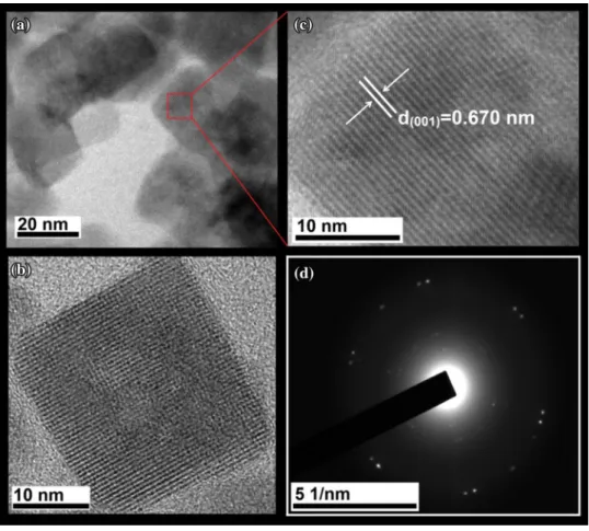
Features such as crystal shape and morphology of Cu2WSe4 nanosheets has been analyzed via TEM and these results has been given in Fig. 2. As shown in Fig. 2a, crys-tal shapes of synthesized nanoparticles are rectangular and square sheet and the average crystal size is between 20 and 40 nm. HR-TEM images are given Fig. 2b, c. Lattice fringes of Cu2WSe4 demonstrated their highly crystalline nature.
Also interplanar spacing of Cu2WSe4 nanosheets were
cal-culated as 0.670 nm which corresponds to (001) plane. SAED image of Cu2WSe4 nanosheets is shown in Fig. 2d. It is understood that SAED diffraction spots matched to tetragonal crystal structure and Cu2WSe4 nanosheets have
single crystalline nature. It is shown that these results com-patible with XRD results.
3.2 Estimation of optical and dielectric parameters of Cu2WSe4 thin film
An interesting application of the theory already discussed is to the phenomena of reflection from and transmission through thin films. In this case there are multiple reflec-tions at both surfaces of the film, and interference effects are present in the reflected and transmitted light. In our dis-cussion, we shall limit ourselves to light that is plane polar-ized in, or normal to, the plane of incidence. Assume that the film is bounded on one side by a dielectric, in which the incident beam is located, and on the other side by any other medium. The measured spectral variations of transmis-sion and reflection of Cu2WSe4 thin film are illustrated in (Fig. 3a). The transmittance spectrum shows that the film
Fig. 1 XRD pattern of Cu2WSe4 nanosheets
has a high transparency (nearly 70%) at the infrared region. Sani et al. [30] have emphasized that several methods for the experimental determination of the optical constants have been proposed and developed in the past. The linear
absorption coefficient has been determined by using both the transmittance and reflectance spectrum of the relation [30, 31].
Fig. 2 a TEM, b, c HR-TEM, d SAED pattern of the Cu2WSe4
nanosheets
Fig. 3 a The spectra of transmittance and reflectance against wavelength, b the (𝛼h𝜈)2 curves against photon energy of Cu
where R is reflectance, Tis transmittance and d is the thickness of film. An important effect, neglected so far, is the interaction between the electron and the hole which are produced when optical absorption causes a transition from a valence band to a conduction band. This interaction can lead to bound states of the electron–hole pair, called excitons, which give characteristic absorption spectra at low tempera-ture. Affect the absorption coefficient near the absorption edge, causing an abrupt increase at the edge, followed by a gradual rise which merges at energies far from the edge into the absorption coefficient that would be calculated without the interaction. To determine the band gap energy of mate-rials, in common, the variation of 𝛼hv with (hv − Eg)n is investigated, where hv is the photon energy, Eg is the optical band gap, and n. is either 1/2 for indirect transition or 2 for direct transition. In many semiconductors the bottom of the conduction band and the top of the valence band are not at the same point. Another interaction mechanism must be present to provide the crystal momentum required for a tran-sition from one of these states to the other. Lattice vibrations can provide this momentum, but other scattering mecha-nisms may sometimes be involved. The theory of this type of transition has been reviewed by [30]. For a participating phonon group with energy near the absorption coefficient contains terms proportional to energy gap. The values of the direct optical band gap Eg is established, as usual, by plotting (𝛼hv)2 as a function of photon energy (hv), which is called (2)
𝛼 = 1 dln
( (1 − R)2 T
) the Tauc’s plot [32, 33]. Fig. 3b shows the plots of (𝛼hv)2
versus (hv). It is clear that (𝛼hv)2= f (hv) is a linear function.
This linearity indicates the existence of allowed direct tran-sitions between the valance band and conduction band. Eg of Cu2WSe4 thin film has been found as 1.64 eV which was
estimated by extrapolation of the linear region of the curves to meet the (hv) axis i.e. (𝛼hv)2= 0. This value is similar to
the earlier report [25]. Kaviyarasu et al. [34] have reported that copper selenide (CuSe) semiconductor quantum dots synthesized by the reflux condensation method. They have applied this method at constant temperature 90 °C for dif-ferent hours 4, 8 and 12 h and direct band gap energy of the copper selenide quantum dots was found to be 1.12, 1.24 and 1.38 eV respectively.
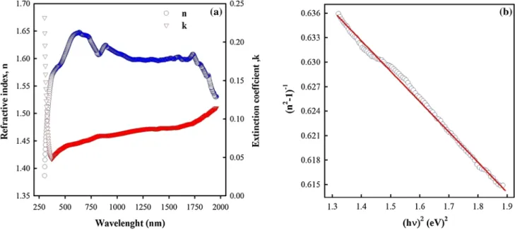
Imaginary part of complex refractive index (n), the extinction coefficient(k), can be calculated directly from the absorption coefficient (𝛼) using the relation of k = 𝛼𝜆∕4𝜋. The spectral variation of refractive index is calculated from
R and k values using the following relation [30],
The wavelength dependence of k and n of the Cu2WSe4
film is given in Fig. 4a. As shown in Fig. 4a, both the values of k and n decrease with the increase of the wavelength in UV–Vis region for the film. The changes of n and k with the increase of wavelength of k, despite the increase in n 1.65 at 600 nm decreased after reaching a maximum value of 1.65 and swinging to a value 1.55 of worth. To represent the (3) n =(1 + R 1 − R ) + √ 4R (1 − R)2 − k 2
Fig. 4 a Representation of the refractive index and extinction coefficient as a function of the wavelength b variation of plot (n2
− 1)−1 with (h𝜈)2
refractive index below the optical band gap in term of energy (or wavelength), the single term Wemple DiDomenico oscil-lator formulae is widely used. Thus, the dispersion relation for the refractive index can be given by [34–36].
where Ed is the dispersion energy, which can be interpreted as a measure of the strength of interband optical transi-tion, and E0 is termed as single oscillator energy. If we plot
(n2− 1)−1
versus (hv)2, a straight linear region is obtained, as
shown in Fig. 4b. The values of E0 and Ed have been evalu-ated from the intercept determined by extrapolation of the line to (n2− 1)−1
axis and the slope, respectively. The values found for E0 and Ed are 4.35 and 6.37 eV, respectively. It seems that, the single oscillator energy E0 is compatible with
an empirical relation such as E0= 2.2 Eg. The static refrac-tive index, n0 can be calculated by n0=√1 + Ed∕E0 as 1.56.
Dielectric constant is essentially a linear treatment, valid for weak fields. Thus methods based on a wavelength-dependent dielectric constant cannot be expected to be valid in the immediate vicinity of the impurity, where the electro-static potential and the electric field will be very strong. The wavelength-dependent dielectric constant does, however, give a more accurate description of the potential far from the impurity, particularly the oscillating term, than does the conventional result. The dielectric function of any material is dependent on its complex refractive index and so, real imagi-nary parts of dielectric function can be given in terms of the refractive index and the extinction coefficient as [29, 37];
(4) (n2− 1)−1= E0 Ed − 1 E0Ed(hv) 2
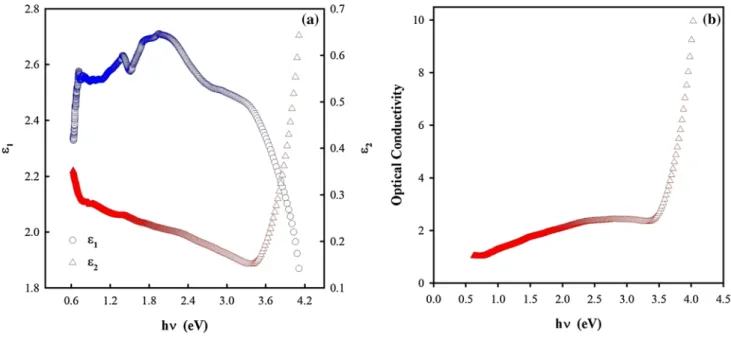
We have plotted the real (𝜀1) and imaginary (𝜀2) part
of dielectric function of photon energy, calculated from n and k values, as a function of wavelength, in Fig. 5a. The main peak in (𝜀2) spectrum corresponds to the fundamental
absorption edge of material energy, which declares normal dispersion in the region. As shown in Fig. 5a., the values of real part of dielectric constant are higher than the imaginary parts for thin film. Similar reviews for real and imaginary part of dielectric function of photon energy were made by Astinchap et al. [38].
The optical conductivity of a material is related to its absorption coefficient by [29],
Figure 5b shows the variation of optical conductivity with the incident photon energy. The optical conductivity shows approximately a linear behavior over a broad part of spectrum. It smoothly increases with the photon energy. The increased optical conductivity at high photon energies (3.52 eV) is due to the high absorbance of Cu2WSe4 thin films in that region.
3.3 Determination of contact parameters of Au/ Cu2WSe4/n‑Si Schottky diode
The Au/Cu2WSe4/n-Si device architecture is shown in
Fig. 6a with an active device area of 0.08 cm. The thick-ness layer of the nanosheets was determined approximately
(5)
𝜀1= n2− k2; 𝜀2 = 2nk
(6)
𝜎opt= 𝛼nc
4𝜋
290 nm. Current–voltage (I–V) characteristics of the diodes provide a beneficial information about the diode parameters such as saturation current (I0), barrier height
(ΦB), ideality factor (n), series resistance (Rs). The meas-ured I–V characteristics of the diode have been evaluated from the conventional Schottky barrier thermionic emis-sion (TE) theory and is given by the relations [38–40]:
where I0 is saturation current, n is the diode quality factor, q is the electronic charge, A is the Schottky diode contact
area, A* is the effective Richardson constant and is equal to 112 A cm− 2 K− 2 for n-type Si [41, 42], T is the absolute
temperature in Kelvin. I0is the saturation current derived
from the straight line intercept of ln I at zero-bias.
The ΦB Schottky barrier height and nideality factor val-ues of Au/Cu2WSe4/n-Si can be determined from
inter-cepts and slopes of the voltage dependent of forward-bias lnI curve respectively [43, 44]. Figure 6b displays the cur-rent–voltage (I–V) characteristics of the Au/Cu2WSe4/n-Si diode at the room temperature. The saturation current (I0) value was determined from the linear portion intercept of lnI–V at V = 0 in the room temperature. The values of the barrier height (ΦB) and ideality factor (n) havebeen determined from the forward I–V characteristics of the diodes given in Fig. 6b using Eq. 8. The determined val-ues of Schottky barrier height (ΦB) and ideality factor (n) for the diode are 0.542 eV and 1.25 respectively. The high ideality factor value of the diode is probably due (7) I = I0 [ exp( qV nkT ) − 1 ] ; I0 = AA∗T2exp ( −qΦB kT )
to a potential drop in the interface layer, the presence of excess current and the recombination current through the interfacial states between the semiconductor and insula-tor layers [42]. Kalenga et al. [2] have reported Schottky diode device fabricated from Cu2 − xSe nanoparticles syn-thesized using the microwave digestive method. They have reported that the thermionic theory using data extracted from the experimental I–V curve resulted in the ideality factor of 4.35 and the barrier height of 0.895 eV whilst the Cheung’s method resulted in the ideality factor, bar-rier height and series resistance of 1.04, 0.00259 eV and 0.870 respectively.
I–V characteristic was plotted on log–log scale to order
to more information about the current conduction proper-ties of Au/Cu2WSe4/n-Si. Figure 6c indicates the double
logarithmic forward bias I–V plots of the Au/Cu2WSe4/n-Si
device at room temperature. As seen in Fig. 6c two distinct regions can be identified, indicating different conduction mechanisms. At low voltages, the slope of the lnI versus
lnV plot is approximately unity. Currents increase linearly
with the voltage in this region. This behavior called as ohmic conduction.
n equals to 1 for an ideal diode. However, n has usually a
value greater than unity. High values of n can be attributed to the presence of the interfacial thin layer, a wide distribution of low-Schottky barrier height (SBH) patches (or barrier (8) ΦB= kT q ln ( AA∗T2 I0 ) and n = q kT dV d ln(I)
inhomogeneities) and to the bias voltage dependence of the SBH [45, 46]. By differentiating this equation with respect to I and rearranging we find that
dV∕d ln(I) versus I plot should yield straight lines in the
downward curvature region of ln I − V plot in accordance with Eq. 8 and its slope gives the series resistance (Rs) and its intercept on the current axis gives nkT∕q.
The Cheung’s method is thought to be the most accurate as it takes into account the series resistance. The obtained values therefore are indicative of good diode behavior of the device and this is a highly sought after goal in all elec-tronic materials development. To obtain barrier height (ΦB), Cheung and Cheung defined a function as [47]
In Fig. 7 we give the plots of dV∕d ln(I) and H(I) ver-sus I for Au/Cu2WSe4/n-Si Schottky barrier diodes at room
temperature. The values of Rs and n were calculated from
dV∕d ln(I) versus I curve, yielding Rs = 17.65 Ω and n = 1.24 for Au/Cu2WSe4/n-Si diode at room temperature. Similarly, the plot of H(I) versus I gives the series resistance and the barrier height ΦB. The values of ΦB and Rs were calculated, yielding values of ΦB = 0.545 eV and Rs = 17.66 Ω for Au/ Cu2WSe4/n-Si Schottky barrier diode at room temperature. (9) dV d ln(I)= nkT q + IRs (10) H(I) = V −( nkT q ) ln( I AA∗T2 ) = nB+ IRs 4 Conclusions
The Cu2WSe4 nanosheets have been successfully
synthe-sized using hot injection method. The XRD patterns exhibit the tetragonal crystal structure of the samples with oriented in the (100) direction and crystal shapes of synthesized nan-oparticles are rectangular and square sheet and the average crystal size is between 20 and 40 nm. The average parti-cle size obtained from TEM micrographs is in agreement with the crystalline size calculated from XRD patterns. The Cu2WSe4 nanoparticles were deposited by spin coating on
glass and n-type Si substrate. The optical absorption spectra of Cu2WSe4 thin film have been studied in the spectral range 250–2000 nm. Some of the important spectral parameters, oscillator energy E0, dispersion energy Ed and static refrac-tive index n0 were calculated. The direct allowed transition
of the film was observed with band gaps of 1.64 eV. The optical dispersion parameters of the Cu2WSe4 are deter-mined by the single oscillator model of Wemple DiDo-menico relations. Where, E0, Ed and n0 are 4.35, 6.37 eV
and 1.56 respectively. The electronic properties of the Au/ Cu2WSe4/n-Si Schottky barrier diode have been investigated by using current–voltage (I–V) characteristics. The param-eters obtained from thermionic model of the diode were compared with those obtain from the Cheung’s method. The ideality factor obtained from the thermionic model was large indicating a deviation from an ideal diode. The value however did not take into account the series resistance which is one of the reasons for deviation from ideality. Cheung’s method resulted in a decrease in the ideality factor to 1.04 with small series resistance being observed. The observed Schottky diode behavior of the Cu2WSe4 nanosheets device
is indicative of its potential use in electronic devices either as transistor, photodetector or solar cell.
References
1. C.J. Crossland, J.S.O Evans, Chem. Commun. 18, 2292–2293 (2003)
2. M.P. Kalenga, S. Govindraju, M. Airo, M.J. Moloto, L.M. Sikh-wivhilu, N. Moloto, J. Nanosci. Nanotechnol. 15, 4480–4486 (2015)
3. R.S. Mane, S.P. Kajve, C.D. Lokhande, S.H. Han, Vacuum 80, 631–635 (2006)
4. V.M. Gracia, P.K. Nair, M.T.S. Nair, J. Cryst. Growth 203, 113– 124 (1999)
5. S.C. Riha, D.C. Johnson, A.L. Prieto, J. Am. Chem. Soc. 133, 1383–1390 (2010)
6. H. Nakanishi, S. Endo, T. Irie, Jpn. J. Appl. Phys. 8, 443–449 (1969)
7. T.R. Wei, H. Wang, Z.M. Gibbs, C.F. Wu, G.J. Snyder, J.F. Li, J. Mater. Chem. A 2, 13527–13533 (2014)
8. D.H. Foster, V. Jieratum, R. Kykyneshi, D.A. Keszler, G. Schnei-der, Appl. Phys. Lett. 99, 181903 (2011)
Fig. 7 dV/d(lnI) − I and H(I) − I characteristics of Au/Cu2WSe4/n-Si
9. W. Li, S. Lin, X. Zhang, Z. Chen, X. Xu, Y. Pei, Chem. Mater. 28, 6227–6232 (2016)
10. C.R. Lin, C.L. Yeh, S.Z. Lu, I.S. Lyubutin, S.C. Wang, I.P. Suzda-lev, Nanotechnology 21, 235603 (2010)
11. D. Kim, A.N. Rusnak, S. Parameswaran, C.R. Patra, V.B. Tro-fimov, R. Harpness, A. Gedanken, Yu..S. Tver’yanovich, Glass Phys. Chem. 32, 330–336 (2006)
12. D.T. Do, S.D. Mahanti, J. Phys. Chem. Solids 75, 477–485 (2014) 13. C.J. Crossland, P.J. Hickey, J.S.O. Evans, J. Mater. Chem. 15,
3452–3458 (2005)
14. H. Liang, L. Guo, Int. J. Hydrog. Energy 35, 7104–7109 (2010) 15. N. Li, M. Liu, Z. Zhou, J. Zhou, Y. Sun, L. Guo, Nanoscale 6,
9695–9702 (2014)
16. P.D. Tran, M. Nguyen, S.S. Pramana, A. Bhattacharjee, S.Y. Chiam, J. Fize, M.J. Field, V. Artero, L.H. Wong, J. Loob, J. Bar-ber, Energy Environ. Sci. 5, 8912–8916 (2012)
17. D. Jing, M. Liu, Q. Chen, L. Guo, Int. J. Hydrog. Energy 35, 8521–8527 (2010)
18. H. Chen, K. Zhang, W. Chen, I. Ali, P. Wu, D. Liu, L. Song, AIP Adv. 5, 037141 (2015)
19. W. Chen, H. Chen, H. Zhu, Q. Gao, J. Luo, Y. Wang, S. Zhang, K. Zhang, C. Wang, Y. Xiong, Y. Wu, X. Zheng, W. Chu, L. Song, Z. Wu, Small 22, 4637–4644 (2014)
20. L.Y. Gan, U. Schwingenschlögl, Phys. Rev 89, 125423 (2014) 21. M. Yıldırım, F. Özel, A. Sarılmaz, A. Aljabour, i.H. Patır, J.
Mater. Sci. 28, 6712–6721 (2017)
22. F. Özel, E. Aslan, A. Sarılmaz, I.H. Patır, ACS Appl. Mater. Inter-faces 8, 25881–25887 (2016)
23. E. Aslan, M.K. Gönce, M.Z. Yiğit, A. Sarılmaz, E. Stathatos, F. Özel, M. Can, İ.H. Patır, Appl. Catal. B 210, 320–327 (2016) 24. M. Kuş, F. Özel, S. Büyükçelebi, A. Aljabour, M. Ersöz, N.S.
Sarıçiftci, Opt. Mater 39, 103–109 (2015)
25. A. Sarılmaz, M. Can, F. Özel, J. Alloys Compd. 699, 479–483 (2017)
26. W. Kern, D.A. Puotinen, P. Scherrer, RCA Rev. 31, 187–206 (1970)
27. P. Scherrer, Mathematisch-Physikalische Klasse 1918, 98–100 (1918)
28. J.I. Langford, A.J.C. Wilson, J. Appl. Cryst 11, 102–113 (1978) 29. B. Corain, G. Schmid, N. Toshima, Metal Nanoclusters in
Cataly-sis and Materials Science: The Issue of Size Control, 1st ed. (Else-vier, Amsterdam, 2008)
30. E. Sani, A. Dell’Oro, Opt. Mater. 60, 137–141 (2016)
31. E.D. Palik, Handbook of Optical Constants of Solids. (Academic Press, California, 1998)
32. M. Yıldırım, F. Özel, N. Tuğluoğlu, Ö.F. Yüksel, M. Kuş, J. Alloy Compd. 666, 144–152 (2016)
33. J. Tauc, J. Non Cryst. Solids 8, 569–585 (1972)
34. K. Kaviyarasu, A. Ayeshamariam, E. Manikandan, J. Kennedy, R. Ladchumananandasivam, U.U. Gomes, M. Jayachandran, M. Maaza, Mater. Sci. Eng. B 210, 1–9 (2016)
35. S.H. Wemple Jr., M. DiDomenico, Phys. Rev. B 3, 1338–1351 (1971)
36. S.H. Wemple Jr., M. DiDomenico, Phys. Rev. B 1, 193–202 (1970)
37. M. Yıldırım, A. Aljabour, A. Sarılmaz, F. Özel, J. Alloys Compd. 722, 420–426 (2017)
38. B. Astinchap, R. Moradian, K. Gholami, Mat. Sci. Semicon. Proc. 63, 169–175 (2017)
39. L.J. Brillson, Surf. Sci. Rep. 2, 123 (1982)
40. S. Sze, Physics of Semiconductor Devices (Wiley, New York, 1981)
41. E.H. Rhoderick, R.H. Williams, Metal-Semiconductor Contacts (Clarendon Press, Oxford, 1988)
42. Ö.F. Yüksel, M. Kuş, M. Yıldırım, J. Electron. Mater 46, 882–887 (2017)
43. G. Topal, A. Tombak, E. Yigitalp, D. Batibay, T. Kılıçcoğlu, Y.S. Ocak, J. Electron. Mater. 46, 3958–3964 (2017)
44. M.A. Lampert, P. Mark, Current Injection in Solids (Academic Press, New York, 1970)
45. Ş. Aydoğan, M. Sağlam, A. Türüt, J. Phys. 18, 2665–2676 (2006) 46. R.T. Tung, Phys. Rev. B 45, 13509 (1992)