PAPER
2D vibrational properties of epitaxial silicene on Ag(111)
Dmytro Solonenko1, Ovidiu D Gordan1, Guy Le Lay2, Hasan Sahin3, Seymur Cahangirov4,
Dietrich R T Zahn1 and Patrick Vogt5
1 Technische Universität Chemnitz, Reichenhainer Straße 70, D-09126 Chemnitz, Germany 2 Aix-Marseille Université, CNRS, PIIM UMR 7345, 13397 Marseille Cedex, France 3 Department of Photonics, Izmir Institute of Technology, 35430 Izmir, Turkey
4 UNAM-National Nanotechnology Research Center, Bilkent University, 06800 Ankara, Turkey 5 Technische UniversitÄt Berlin, Hardenbergstraße 36, D-10623 Berlin, Germany
E-mail:[email protected]
Keywords: epitaxial silicene, phonon modes, in situ Raman spectroscopy, ab initio theory Supplementary material for this article is availableonline
Abstract
The two-dimensional silicon allotrope, silicene, could spur the development of new and original
concepts in Si-based nanotechnology. Up to now silicene can only be epitaxially synthesized on a
supporting substrate such as Ag(111). Even though the structural and electronic properties of these
epitaxial silicene layers have been intensively studied, very little is known about its vibrational
characteristics. Here, we present a detailed study of epitaxial silicene on Ag(111) using in situ Raman
spectroscopy, which is one of the most extensively employed experimental techniques to characterize
2D materials, such as graphene, transition metal dichalcogenides, and black phosphorous. The
vibrational
fingerprint of epitaxial silicene, in contrast to all previous interpretations, is characterized
by three distinct phonon modes with A and E symmetries. Both, energies and symmetries of theses
modes are confirmed by ab initio theory calculations. The temperature dependent spectral evolution
of these modes demonstrates unique thermal properties of epitaxial silicene and a significant
electron–phonon coupling. These results unambiguously support the purely two-dimensional
character of epitaxial silicene up to about 300
°C, whereupon a 2D-to-3D phase transition takes place.
The detailed
fingerprint of epitaxial silicene will allow us to identify it in different environments or to
study its modifications.
1. Introduction
The successful growth of silicene, the first purely synthetic elemental 2D honeycomb material, was reported in 2012 on a Ag(111) single crystal [1–3],
ZrB2 [4], and later on Ir(111) [5] templates. Yet,
Ag(111) is by far the most used substrate material for the growth of silicene and it is the subject of most theoretical investigations. The archetype and best investigated epitaxial silicene structure on Ag(111), develops a 3×3 reconstruction coinciding with a 4×4 Ag(111) surface supercell (in short termed
´ ´
(3 3) (4 4)) [1]. Various experimental
techni-ques have been applied to study this seminal silicene phase, such as scanning tunneling microscopy and spectroscopy(STM and STS) [1–3], non-contact atomic
force microscopy [6], as well as electron diffraction
(LEED and RHEED), photoemission spectroscopy
[1,7, 8], and large scale surface diffraction methods
[9,10]. The suggested atomic model for this epitaxial
silicene layer is supported by ab initio calculations which also reveal a sp2/sp3character of the single Si atoms[1,11]. Apart from these achievements, a detailed
picture of the vibrational properties of epitaxial silicene is still missing including a clear assignment of the phonon symmetries, their temperature dependence, an assignment to the atomic motion of the phonons, and an experimental indication for the strength of the electron–phonon coupling. Raman spectroscopy allows these properties to be determined and has been one of the most extensively employed experimental techni-ques to study graphene[12] and 2D layered materials
like transition metal dichalcogenides (TMDCs) [13]
and black phosphorous[14].
Here, we report a thorough and comprehensive Raman study carried out in situ to fully characterize RECEIVED
29 July 2016
REVISED
4 October 2016
ACCEPTED FOR PUBLICATION
17 October 2016
PUBLISHED
28 October 2016
stacks, and the analysis of structural changes upon functionalization of epitaxial silicene by atomic and molecular species.
2. Experimental and theoretical details
Clean, well-ordered Ag(111) surfaces were prepared by Ar+-bombardment (1.5 kV, 5·10−5 mbar) and subsequent annealing at ~530 C of (111)-oriented Ag single crystals under ultra-high vacuum conditions (base pressure ~2.0 10· -10 mbar). Si was deposited
by evaporation from a directly heated Si-wafer piece, while the Ag sample was kept at a constant temper-ature, adjustable between 20°C and 500 °C with a precision of 10 C. The symmetry of the Si layer and the related phase composition was carefully checked after preparation by low-energy electron diffraction (LEED). In agreement with previous results [1] the
preparation conditions were chosen adequately to produce a dominating(3´3) (4´4 epitaxial sili-) cene phase. STM measurements were performed at room temperature in constant-current mode using an Omicron VT-STM with an electrochemically etched tungsten tip. The morphology of the Ag crystal and the differently prepared Si layers was probed by atomic force microscopy (AFM) (AFM 5420, Agilent Tech-nologies Inc.) with commercial tips (curvature radius 10 nm) in non-contact mode. In situ Raman measure-ments were performed in macro configuration, col-lecting the scattered light through the transparent port of a UHV chamber in front of the sample and recorded via a Dilor XY 800 monochromator. For excitation the Ar+514.5nm(2.4 eV) laser line was used with a power density of 103W/cm2and an instrumental broadening of 2.5 cm−1. Prior to the experiments we checked that heating of the silicene layer by the laser excitation can be neglected. All experiments were performed at room temperature, unless stated otherwise.
First-principles calculations were performed using the VASP software [15]. We utilize
projector-aug-mented wave potentials[16] for ion-electron
interac-tion and the exchange-correlainterac-tion potential is approximated by the Perdew, Burke, and Ernzerhof (PBE) functional [17]. The cutoff energy of the
plane-wave basis set was chosen to be 320 eV. First, we per-formed a geometry optimization of(3×3) silicene on
used the PHON software[19] to determine the atomic
displacements necessary to construct the dynamical matrix. Then we calculated forces due to these dis-placements in a (2×2) supercell of the (3×3)/ (4×4) system having silicene on top of three Ag(111) layers. This supercell has 72 Si and 192 Ag atoms. The calculated forces are then used as input in the PHON program to calculate the phonon dispersions. Note that, here we separate the vibrational modes of Si and Ag atoms while in fact they move collectively. There-fore, we need to account for the fact that the vibra-tional frequencies of the Si-Ag system is inversely proportional to the square root of the reduced mass given by(m mSi Ag) (mSi+mAg)while in the pure Si system it is inversely proportional to the square root of the mass of the Si atoms, mSi. Hence, we multiplied the
obtained frequencies by mSi+mAg mAg, where mSiand mAgare the total masses of Si and Ag atoms
present in the calculation.
3. Results and discussion
3.1. Vibrational signature of(3´3) (4´4) epitaxial silicene
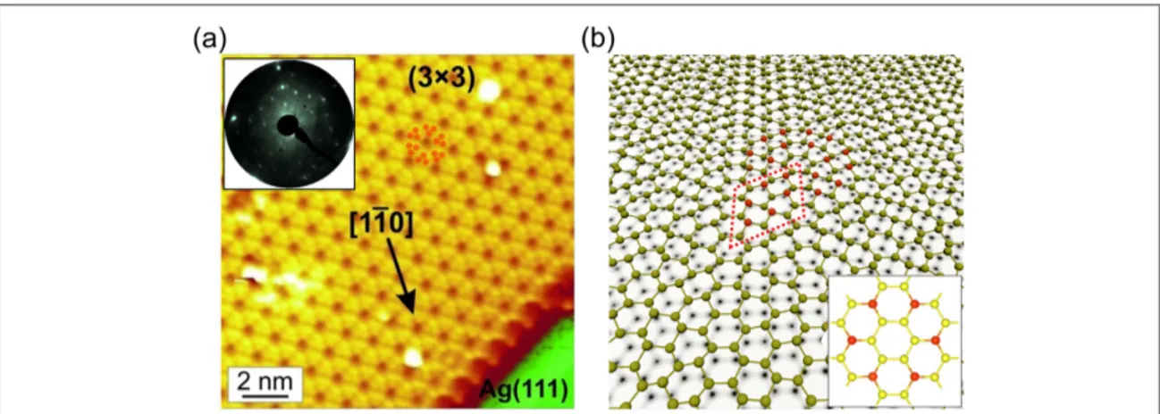
At a deposition temperature of approximately 220°C the archetype (3´3) (4´4 2D epitaxial silicene) phase forms, showing in STM images (figure 1(a),
filled-states) the characteristic flower-like pattern of a regular and well-ordered(3´3 atomic structure, in) agreement with our previous results[1]. Figure 1(b)
shows the atomic ball-and-stick model for this layer. The Si atoms within the (3´3) unit cell show different displacements in the z-direction depending on their position. In the topographic STM image only the top atoms are imaged(red balls), producing the flower-like pattern. Within this structure most of the hexagons are oriented out-of-plane, while only the ones at the dark center of theflower pattern are in-plane. The latter can be used to construct a Wigner-Seitz cell of the epitaxial silicene superstructure (figure1(b), inset), which clearly shows the hexagonal
symmetry of the layer.
Figure2(a) shows an overview Raman spectrum of
the epitaxial(3´3) (4´4 silicene phase recorded) in situ, at room temperature. The observed narrow Raman modes at 175 cm−1, 216 cm−1, and 514 cm−1
underline the crystalline nature of epitaxial silicene. The presence of the broad bands at 350 cm−1and 480 cm−1 is associated with the co-existence of smaller amounts of amorphous Si(a-Si). This assumption is substantiated by the Si deposition on the Ag(111) sur-face at room temperature and oxidation of the epitax-ial silicene (see supplemental material). Therefore, these broad Raman bands are not related to the relaxa-tion of the momentum conservarelaxa-tion law in an epitax-ial silicene layer[21,22].
The small intensity of the a-Si signature indicates that only a minor amount of a-Si is formed, probably at defective substrate areas. In order to obtain the pure spectralfingerprint of epitaxial(3´3) (4´4 sili-) cene infigure2(b) the signature of a-Si was subtracted
from the spectrum displayed infigure2(a). Therefore
the signature of a-Si was obtained after deposition of Si onto Ag(111) at room temperature. This spectrum was subtracted after adjusting the intensity in order to match the broad band at 480 cm−1in the Raman spec-tra of epitaxial silicene. In addition to the intense pho-non modes at 175 cm−1, 216 cm−1, and 514 cm−1, a weak broad band around 410 cm−1can now be seen in the spectrum. This mode matches the spectral range, where a second-order phonon band of the intense mode at 216 cm−1can be expected.
In order to examine the nature of the observed modes at 175 cm−1, 216 cm−1, and 514 cm−1, Raman selection rules were measured in two polarization geo-metries:z xx z¯ ( ) and ¯ ( )z yx z(Porto notation), i.e.
par-allel and crossed polarisations, respectively. The axes represent the sample coordinate system, where the z axis is normal to the substrate surface, while x(aligned with the Ag[-110] direction) and y represent the in-plane axes. Infigure2(c) the Raman spectra for both
geometries are shown together with the fitted line shapes of the single components. The two Raman modes at 175 cm−1and 216 cm−1are clearly visible in parallel geometry but they disappear completely in crossed geometry while the mode at 514 cm−1, as well
as the broad band at 410 cm−1are present in both polarization geometries. Such behaviour is governed by different symmetries of the lattice vibrations asso-ciated with these modes. The(3´3) (4´4 struc-) ture of the epitaxial silicene layer belongs to the C6v symmetry point group[23], which possesses the
fol-lowing possible phonon symmetries: A(z), E1, and E2.
= = = - - -( ) ⎛ ⎝ ⎜ ⎜ ⎞ ⎠ ⎟ ⎟ ⎛ ⎝ ⎜⎜ ⎞⎠⎟⎟ ⎛ ⎝ ⎜ ⎜ ⎞ ⎠ ⎟ ⎟ A z a a b E c c c c E d d d d 0 0 0 0 0 0 ; 0 0 0 0 0 ; 0 0 0 0 0 1 2
It is found that A modes appear only in the parallel geometry while the E modes appear in both geome-tries. Thus, the polarization-dependent Raman results conclusively show that the modes at 175 cm−1and 216 cm−1are fully symmetric vibrations and are assigned to an A symmetry, denoted as A1and A2, respectively. A mode similar to A2 was also observed by in situ Raman measurement at 77 K and related to light scat-tering from domain boundaries [22]. Hence it was
assigned to a‘D band’, by analogy to graphene. This, however, is fully contradictory to ourfindings. The very clear assignment of A1and A2to an A symmetry rules out such explanations, since for the light scatter-ing from the domain boundaries a polarization dependence should not be observed, because they break the long-range translational symmetry in the 2D crystal. The Raman band at 410 cm−1shows a weaker polarization dependence expected for a second order phonon band. The mode at 514 cm−1is assigned to an E symmetry based on the observed polarization dependence. This phonon mode was also reported in previous ex situ and in situ Raman measurements at 516 cm−1 and 530 cm−1, respectively[21, 22]. The
blueshift in the latter case can be partly related to the lower temperature of 77 K during the measurements but the total shift is too large to relate it solely to Figure 1.(a) STM image (Ubias=−1.0 V, I=1.08 nA) of epitaxial(3´3) (4´4 silicene) (reproduced from Vogt P et al 2014 Appl. Phys. Lett.104 021602[20], with the permission of AIP Publishing. At the bottom right corner a part of the bare Ag(111) 1×1
surface can be seen.(b) Atomic ball-and-stick model for(3´3) (4´4 silicene) (adapted from ([1])). The(3´3 unit cell is) indicated by a red rhombus. Inset: the Wigner-Seitz cell of epitaxial silicene. The red spheres represent up-buckled Si atoms of the flower pattern.
thermal effects. In any case, our results provide now experimental evidence for the E symmetry of this mode.
It is remarkable that the Raman signature of epi-taxial(3´3) (4´4 silicene is dominated by pho-) nons with an A symmetry. A modes do not exist in diamond-like Si[24,25] or other bulk Si allotropes.
Due to the 2D nature of the silicene lattice, the transla-tional symmetry is broken perpendicular to the lattice plane. This lifts the phonon triple degeneracy at theΓ point, as it was shown by theoretical calculations for the phonon dispersion of freestanding silicene [26– 28], where the former TO phonon mode of bulk Si
shifts to lower energy. Moreover, according to group theory analysis[29], freestanding silicene has
Raman-active modes of A and E symmetries, unlike bulk Si, which has only one zone-centre Raman mode of F symmetry. We stress that the appearance of A modes in the case of(3´3) (4´4 silicene on Ag(111) is a) conclusive indication of the 2D character of epitaxial silicene. These A modes are associated with an out-of-plane displacement of Si-atoms, a vibrational mode that is supported by the buckling and the out-of-plane
oriented hexagons of the (3´3) (4´4 atomic) structure(figure1(b)). Such modes are not observed
for the fully-planar structure of graphene.
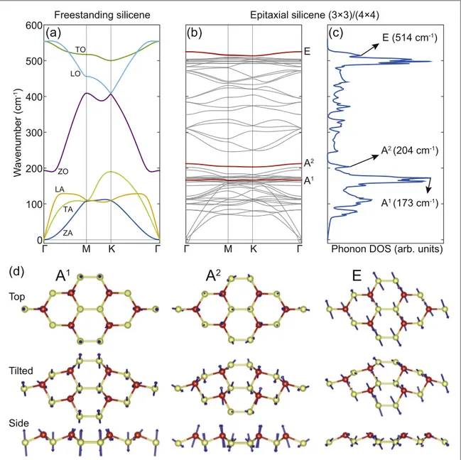
The symmetries of the observed Raman modes are in good agreement with theoretical expectations for freestanding silicene, while their frequencies show much less agreement with available calculations of the phonon dispersion[26–28]. DFT calculations suggest
the presence of three optical phonon branches atΓ: a ZO mode, related to out-of-plane optical phonons, and energetically degenerate TO and LO phonons. While the position of the ZO branch atΓ, is close to the experimentally observed A modes, the degenerate TO/LO branches (562 cm−1[26], ∼550 cm−1 [27],
∼556 cm−1[28]) do not match the E mode of epitaxial
silicene(514 cm−1) (see also figure3(a)). Such a
dis-crepancy can be explained by the significant interac-tion between the Si adlayer and the substrate, the different atomic arrangement caused by the super-structure formation of (3 ´3) (4 ´4) silicene, and the related modified hybridization state with respect to freestanding silicene [11]. To resolve
these discrepancies, we performed ab initio phonon Figure 2.(a) Raman spectrum of(3´3) (4´4 silicene up to 1200 cm) −1. The broad shoulder around 480 cm−1is associated with small amounts of co-existing a-Si. This component is subtracted in(b), clearly showing the phonon modes at 175 cm−1, 216 cm−1, 410 cm−1, and 514 cm−1(FWHM in brackets). (c) Related Raman selection rules for parallel ¯ ( )z xx z and crossed ¯ (z yx z geometries.)
calculations of the (3×3) silicene by taking into account the effect of the Ag(111) substrate on the vibrational properties.
Infigure3(b), we present the calculated phonon
dispersion of(3×3) silicene on Ag(111) obtained by the method described above. The small imaginary fre-quencies near theΓ point are numerical artefacts. For comparison, we also present the phonon dispersion of freestanding silicene calculated with similar para-meters in figure 3(a). The interaction with the
sub-strate alters the phonon dispersions significantly. In particular, the phonon dispersions of the epitaxial sili-cene becomeflat compared to the freestanding case. This is due to the 3×3 reconstruction that breaks the symmetry and forms protruding triplets of Si atoms that are rather isolated from each other. These triplets are involved in all vibrational modes but due to the
isolation the modes becomeflat. The calculated pho-non density of states(DOS) is presented in figure3(c).
Note that, the DOS is not directly correlated to the experimentally observed Raman spectra, as it also includes the contributions from the non-Raman-active phonons. Analysing the symmetries of the opti-cal modes below 220cm−1we indeed encounter only
two normal modes that belong to the irreducible representation A. These modes are highlighted with red lines and denoted as A1and A2infigure3(b). Peaks
attributed to the modes A1 and A2 are centered at 173cm−1and 204cm−1, respectively. In accordance with our experimental data, we see that the frequencies of the degenerate LO/TO modes at the Γ-point are significantly lowered upon the superstructure forma-tion. Symmetry analysis of these degenerate modes shows that they indeed belong to the irreducible Figure 3.(a) Phonon dispersion of freestanding buckled silicene. Longitudinal, transverse and out-of-plane acoustic (and optic) modes are denoted as LA, TA and ZA(LO, TO and ZO), respectively. (b) Phonon dispersion of (3×3) silicene calculated by including the effect of the Ag(111) substrate. The Raman active modes are shown by red lines. (c) Calculated phonon density of states of (3×3) silicene on Ag(111). (d) Top, tilted and side views of eigenvectors of calculated phonon modes identified as the experimentally observed Raman active modes.
of the doubly degenerate E vibrational modes are pre-sented infigure3(d). In the A1mode, the protruding six atoms(forming the ‘flower pattern’) and the six atoms connected to them to form two hexagons are moving down while the remaining six atoms move up. Another way to describe this mode is to look at the inset offigure1(b) and imagine the six atoms forming
the yellow hexagon in the middle moving up while the rest are moving down. In the A2mode, the protruding six atoms move up while the remaining twelve atoms move down. The A1and A2modes are clearly related to the ZO mode of freestanding silicene. For the E mode, the three protruding atoms in the left half of the (3×3) cell move in a certain in-plane direction while the atoms surrounding them move in the opposite direction. The atoms in the right half move opposite to the corresponding atoms in the left half of the(3×3) cell. Hence, both A phonon modes are dominated by out of plane and the E mode by in plane atomic dis-placements supporting the experimentally observed Raman selection rules. The presented agreement allows the experimentally observed Raman modes to be associated with the vibrations described in figure3(d).
We emphasize that the Raman observations give no indication for Si-Ag vibrational modes, resulting from inter-atomic bonding between these two species. Theoretical calculations show that a Si-Ag related mode should evolve at about 90 cm−1[30]. While it
was suggested that Si-Ag bonds, or even alloying, could play a role for some of the Si phases on Ag(111) [31], this is not at all observed for (3´3) (4´4) silicene/Ag(111). However, the interaction with the Ag substrate has a significant effect on the structure and vibrational modes of silicene, as shown by our DFT calculations.
3.2. Temperature dependence and phase transition Figure4(a) shows a series of Raman spectra measured
during the annealing of the epitaxial(3´3) (4´4) silicene layer on Ag(111). The Raman spectra were recorded in incremental temperature steps from room temperature to 500°C. For temperatures up to ~300 C the overall spectral line shape remains unchanged and all modes shift almost equally towards lower wavenumbers with increasing temperature.
of the mode at 520 cm clearly demonstrate that a structural phase transition takes place at temperatures around 300°C in agreement with earlier results [35,36]. According to the Raman spectra, the silicene
layer transforms into a phase which exhibits a bulk Si-like Raman spectrum characterized by the L(T)O mode at 520 cm−1with an asymmetric shoulder on the lower energy side. AFM images acquired at room temperature after the annealing procedure to 500°C (figure4(c)) show the formation of small islands with
an average size of(10 ± 8) nm, distributed over the Ag surface. These islands are not observed on the initial Ag(111) surface (figure4(b)) or after formation of the
epitaxial silicene layer and are, thus, assigned to Si crystallites or Si nanoparticles. This assignment is justified since Si nanoparticles show a L(T)O mode around 520 cm−1 with an asymmetric shoulder, caused by spatial phonon confinement in particles smaller than 7 nm[37], while their size distribution
explains the broad linewidth of this mode. In figure4(d) the room temperature Raman spectrum of
the same sample is shown in a spectral range between 100 cm−1and 1000 cm−1. Note that in this instance, i.e. after formation of Si crystallites, a broad band (2nd-order of the L(T)O mode) centered around 950 cm−1can be seen, which is not the case for the epitaxial silicene layer. This means that the occurrence of this 2nd-order band is indicative for the formation of Si crystallites.
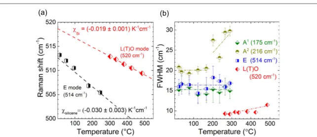
Additional evidence for a phase transition can be found by following the behaviour of the Raman modes upon heating. The temperature-dependent position of the E mode is depicted in figure 5(a). The shift
with increasing temperature allows the determination of its thermal coefficient, having a value of
c = -( 0.0300.003) K
-silicene 1 cm−1. Instead, the thermal coefficient of the L(T)O phonon of the Si nanocrystallites after the phase transition is found to be c = -Si ( 0.0190.003) K-1 cm−1, in good
agreement with values reported for diamond-like bulk Si[25,34,38]. Note, the determination of the thermal
coefficient of silicene is not dependent on absolute temperature and hardly influenced by the external fac-tors such as the underlying Ag substrate. The shift of the other Raman modes of epitaxial silicene (not shown) is similar to the one of the E mode. This reveals that the thermal coefficient of the Raman modes of
epitaxial silicene on Ag(111) markedly differs from the one of bulk-like Si. A similar difference is found between graphene(2D) and diamond (3D), where the zone-centre G mode of graphene has a higher thermal coefficient compared to the diamond phonon mode[32].
3.3. Electron–phonon coupling in epitaxial silicene Further information is gained upon studying the evolution of the FWHM of the silicene Raman modes (figure5(b)). While the widths of the A1(∼15 cm−1)
and the E(∼16 cm−1) modes remain unchanged up to
300°C, the A2mode shows a constant width (~20 cm−1) for temperatures up to 220 °C. For tempera-tures exceeding 240°C the A2mode starts to broaden simultaneously with the appearance of the L(T)O mode(originating from the Si nanoparticles). Moder-ate dewetting of Si atoms from the Ag surface creModer-ates local disorder[35], which could be related to the A2
mode broadening. Remarkably, only the A2 mode responds to this structural change, showing simila-rities to the broadening of the D band of graphene upon temperature increase [12]. At temperatures
above 300°C, we can only follow the FWHM of the Figure 4.(a) Series of Raman spectra of(3´3) (4´4 silicene measured at increasing temperatures.) (b) AFM image (2 μm×2 μm) of the initial Ag(111) surface. (c) AFM image (2 μm×2 μm) after annealing the(3´3) (4´4 silicene layer to 500) °C with small islands(in red). (d) Overview Raman spectra of the epitaxial silicene before and after annealing to 500 °C both measured at room temperature(FWHM in brackets). Inset: detailed Raman spectra (450–550 cm−1).
Figure 5.(a) Raman shift of the E mode of(3´3) (4´4 silicene as a function of temperature.) (b) Full width at half maximum (FWHM) of the silicene A1, A2, and E and the Si L(T)O Raman modes as a function of temperature (with error bars). The experimental points are linearlyfitted (dash-dot lines) and weighted by the error bars.
phonon interaction[12].
Overall, all observed Raman modes for epitaxial
´ ´
(3 3) (4 4) silicene show a markedly larger broadening at room temperature than, for example, the L(T)O mode of bulk Si (∼2.4 cm−1). Beside the already mentioned EPC this broadening could also be caused by a loss of crystallinity and lattice disorder or confinement effects due to small domain sizes. How-ever, the very clear polarization dependence of the phonon modes(described above) and the well defined layer periodicity (according to LEED and STM) demonstrate that disorder as an explanation of the phonon broadening can be neglected. Phonon con-finement could occur if the average domain size of the epitaxial silicene is in the range of a few nm(∼7 nm for Si allotropes [40]). This would lead to a lifting of
momentum conservation which disagrees again with the clear fulfilment of the Raman selection rules. Addi-tionally, the lifting of momentum conservation implies an averaging over the phonon dispersion curves from theΓ point towards the Brillouin zone edge. The branches of optical phonons usually have a negative slope around theΓ point and such averaging would cause an asymmetry of the phonon modes in the case of a significant slope. Since a peak asymmetry is not observed(as it would be expected for Si allo-tropes[27]), phonon confinement cannot explain the
phonon broadening of epitaxial silicene either. Ulti-mately, the large linewidth of the silicene phonon modes and their temperature-independent linewidth character indicate a strong electron–phonon coupling in epitaxial silicene. A very similar effect was shown to introduce a significant broadening of G and G’ pho-non bands of graphene and carbon nanotubes up to 11–13 cm−1 [12,41]. By analogy with the constant
width of the G mode of graphene versus temperature, we also observe a constant linewidth with temperature of the A and E modes, which supports the existence of strong coupling. Significant electron–phonon cou-pling at theΓ point was also predicted theoretically for freestanding silicene[28].
4. Conclusions
To summarize, we have revealed and identified the intrinsic Raman spectral signatures of epitaxial silicene
epitaxial silicene monolayer are limited within a restricted temperature range. At 300°C a dewetting transition takes place and diamond-like Si nanocrys-tals are formed.
Acknowledgments
This work wasfinancially supported by the Deutsche Forschungsgemeinschaft (DFG) under Grant No. VO1261/3-1 and VO1261/4-1, the International Research Training Group(GRK 1215), jointly spon-sored by the DFG and the Chinese Ministry of Education, and the 2D-NANOLATTICES project within the 7th Framework Programme for Research of the European Commission, under FET-Open Grant No. 270749. SC acknowledgesfinancial support from the Scientific and Technological Research Council of Turkey (TUBITAK) under the project number 115F388.
References
[1] Vogt P, De Padova P, Quaresima C, Avila J, Frantzeskakis E, Asensio M C, Resta A, Ealet B and Le Lay G 2012 Phys. Rev. Lett.
108 155501
[2] Lin C L, Arafune R, Kawahara K, Tsukahara N, Minamitani E, Kim Y, Takagi N and Kawai M 2012 Appl. Phys. Express5 045802
[3] Feng B, Ding Z, Meng S, Yao Y, He X, Cheng P, Chen L and Wu K 2012 Nano Lett.12 3507–11
[4] Fleurence A, Friedlein R, Ozaki T, Kawai H, Wang Y and Yamada-Takamura Y 2012 Phys. Rev. Lett.108 245501
[5] Meng L et al 2013 Nano Lett.13 685–90
[6] Resta A, Leoni T, Barth C, Ranguis A, Becker C, Bruhn T, Vogt P and Le Lay G 2013 Sci. Rep.3 2399
[7] Padova P D et al 2013 Appl. Phys. Lett.102 163106
[8] Avila J, Padova P D, Cho S, Colambo I, Lorcy S, Quaresima C, Vogt P, Resta A, Lay G L and Asensio M C 2013 J. Phys. Cond. Matt.25 262001
[9] Takagi N, Lin C L, Kawahara K, Minamitani E, Tsukahara N, Kawai M and Arafune R 2015 Prog. Surf. Sci.90 1–20
[10] Fukaya Y, Mochizuki I, Maekawa M, Wada K, Hyodo T, Matsuda I and Kawasuso A 2013 Phys. Rev. B88 205413
[11] Cahangirov S, Audiffred M, Tang P, Iacomino A, Duan W, Merino G and Rubio A 2013 Phys. Rev. B88 035432
[12] Ferrari A C 2007 Solid State Commun.143 47–57
[13] Li H, Zhang Q, Yap C C R, Tay B K, Edwin T H T, Olivier A and Baillargeat D 2012 Adv. Func. Mat22 1385–90
[14] Xia F, Wang H and Jia Y 2014 Nat. Commun.5 4458
[15] Kresse G and Furthmüller J 1996 Phys. Rev. B54 11169–86
[16] Blöchl P E 1994 Phys. Rev. B50 17953–79
[17] Perdew J P, Burke K and Ernzerhof M 1996 Phys. Rev. Lett.77 3865–8
[18] Cahangirov S S, Topsakal M, Aktürk E, Şahin H and Ciraci S 2009 Phys. Rev. Lett.102 236804
[19] Alfe D 2009 Comput. Phys. Commun.180 2622–33
[20] Vogt P, Capiod P, Berthe M, Resta A, De Padova P, Bruhn T, Le Lay G and Grandidier B 2014 Appl. Phys. Lett.104 021602
[21] Cinquanta E, Scalise E, Chiappe D, Grazianetti C, van den Broek B, Houssa M, Fanciulli M and Molle A 2013 J. Phys. Chem. C117 16719–24
[22] Zhuang J, Xu X, Du Y, Wu K, Chen L, Hao W, Wang J, Yeoh W K, Wang X and Dou S X 2015 Phys. Rev. B91 161409
[23] Pflugradt P, Matthes L and Bechstedt F 2014 Phys. Rev. B89 035403
[24] Richter H, Wang Z P and Ley L 1981 Solid State Commun.39 625–9
[25] Menéndez J and Cardona M 1984 Phys. Rev. B29 2051–9
[26] Yan J A, Stein R, Schaefer D M, Wang X Q and Chou M Y 2013 Phys. Rev. B88 121403
[27] Gori P, Pulci O, Vollaro R d L and Guattari C 2014 Energy Procedia45 512–7
[28] Li X, Mullen J T, Jin Z, Borysenko K M,
Buongiorno Nardelli M and Kim K W 2013 Phys. Rev. B87 115418
[29] Ribeiro-Soares J, Almeida R M, Cançado L G,
Dresselhaus M S and Jorio A 2015 Phys. Rev. B91 205421
[30] Chou S H, Freeman A J, Grigoras S, Gentle T M, Delley B and Wimmer E 1988 J. Chem. Phys.89 5177–89
[31] Prévot G, Bernard R, Cruguel H and Borensztein Y 2014 Appl. Phys. Lett.105 213106
[32] Calizo I, Balandin A A, Bao W, Miao F and Lau C N 2007 Nano Lett.7 2645–9
[33] Sahoo S, Gaur A P S, Ahmadi M, Guinel M J F and Katiyar R S 2013 J. Phys. Chem. C117 9042–7
[34] Hart T R, Aggarwal R L and Lax B 1970 Phys. Rev. B1 638–42
[35] Acun A, Poelsema B, Zandvliet H J W and Gastel R v 2013 Appl. Phys. Lett.103 263119
[36] Liu Z L, Wang M X, Liu C, Jia J F, Vogt P, Quaresima C, Ottaviani C, Olivieri B, Padova P D and Lay G L 2014 APL Materials2 092513
[37] Campbell I H and Fauchet P M 1986 Solid State Commun.58 739–41
[38] Périchon S, Lysenko V, Remaki B, Barbier D and Champagnon B 1999 J. Appl. Phys.86 4700–2
[39] Mishra P and Jain K P 2000 Phys. Rev. B62 14790–5
[40] Mishra P and Jain K P 2001 Phys. Rev. B64 073304
[41] Lazzeri M, Piscanec S, Mauri F, Ferrari A C and Robertson J 2006 Phys. Rev. B73 155426