Nanoscale
www.rsc.org/nanoscaleISSN 2040-3364
PAPER
PAPER
Cite this:Nanoscale, 2016, 8, 4495
Received 28th July 2015, Accepted 23rd September 2015 DOI: 10.1039/c5nr05063d www.rsc.org/nanoscale
Flexible and fragmentable tandem photosensitive
nanocrystal skins
†
S. Akhavan,
aC. Uran,
aB. Bozok,
aK. Gungor,
aY. Kelestemur,
aV. Lesnyak,
b,cN. Gaponik,
bA. Eychmüller
band H. V. Demir*
a,dWe proposed and demonstrated thefirst account of large-area, semi-transparent, tandem photosensitive nanocrystal skins (PNSs) constructed onflexible substrates operating on the principle of photogenerated potential buildup, which avoid the need for applying an external bias and circumvent the current-matching limitation between junctions. We successfully fabricated and operated the tandem PNSs com-posed of single monolayers of colloidal water-soluble CdTe and CdHgTe nanocrystals (NCs) in adjacent junctions on a Kapton polymer tape. Owing to the usage of a single NC layer in each junction, noise generation was significantly reduced while keeping the resulting PNS films considerably transparent. In each junction, photogenerated excitons are dissociated at the interface of the semi-transparent Al elec-trode and the NC layer, with holes migrating to the contact elecelec-trode and electrons trapped in the NCs. As a result, the tandem PNSs lead to an open-circuit photovoltage buildup equal to the sum of those of the two single junctions, exhibiting a total voltage buildup of 128.4 mV at an excitation intensity of 75.8μW cm−2at 350 nm. Furthermore, we showed that theseflexible PNSs could be bent over 3.5 mm radius of curvature and cut out in arbitrary shapes without damaging the operation of individual parts and without introducing any significant loss in the total sensitivity. These findings indicate that the NC skins are promising as building blocks to make low-cost,flexible, large-area UV/visible sensing platforms with highly efficient full-spectrum conversion.
1.
Introduction
Solution-processed semiconductor nanocrystals (NCs) are praised for the capabilities they offer for color tuning and large-area surface coverage as well as the possibility for low-cost fabrication of flexible active device platforms.1This makes them ideal as a photoactive absorbing layer in photosensors.2 The photosensitivity of solution-cast NC photodetectors, either in photoconductor or photodiode architecture, is quite impressive with high photoconductive gain and low noise.3,4 Fabrication of solution-processed photodetectors with high sensitivity and good response including ultrasensitive and fast detection has been reported.5,6 In these conventional NC-based photodetectors, external bias must be applied to
separate and collect the photogenerated charges. Although photodetectors comprising Shockley–Schottky barriers can be principally operated without an applied bias (in the open-circuit mode), this would commonly come at the cost of substantially decreasing their sensitivity. Nevertheless, they are usually operated under negative bias and exhibit a dark current, which results in noise levels limiting the device’s detection capabilities. Furthermore, the required external bias may affect the photoactive layers causing defects that lead to device degradation.7
Given that the performance efficiency of photosensors is strongly dependent on the fraction of photons absorbed, there is a compromise on the thickness of the photoactive layer, which is still a challenge for the electronic properties of NC solids. Indeed, the active region thickness is restricted in the order of, or considerably less than, 100 nm due to the relatively short minority carrier diffusion length within the NCs.8 There-fore, to enhance the absorbance, increasing the film thickness is not a useful approach since it may exceed the diffusion length.9 Likewise, this fundamental trade-off reduces the device transparency and influences the noise generation-recombination. Thus, the use of a photoactive layer as thin as possible is especially advantageous for avoiding the self-absorption effect.
†Electronic supplementary information (ESI) available. See DOI: 10.1039/ c5nr05063d
aUNAM–Institute of Materials Science and Nanotechnology, Department of Electrical
and Electronics Engineering, and Department of Physics, Bilkent University, Ankara, 06800, Turkey
bPhysical Chemistry, Technische Universität Dresden, Dresden, 01062, Germany c
Department of Nanochemistry, Istituto Italiano di Tecnologia, Genova, 16163, Italy
dSchool of Electrical and Electronic Engineering and School of Physical and
Mathematical Sciences, Nanyang Technological University, Singapore, 639798, Singapore. E-mail: [email protected]
Published on 30 September 2015. Downloaded by Bilkent University on 12/23/2018 10:45:41 AM.
View Article Online
To overcome the aforementioned challenges for solution-processed light-sensitive devices, photosensitive nanocrystal skins (PNSs) were demonstrated consisting of single mono-layer colloidal NCs. These PNSs offer the potential of high sen-sitivity for large-area applications as they operate on the principle of photogenerated voltage buildup in the absence of an external bias.10Owing to the single NC layer in the device structure, noise generation is significantly reduced, enhancing the device sensitivity.11In operation, photogenerated excitons are not allowed to pass directly through the device. With exciton dissociation due to the difference between the work functions of the NCs and the metal contact, holes migrate to the metal contact while most of the electrons are trapped inside the NCs, leading to a potential buildup across the device. When light irradiates the PNS, it passes through the monolayer of the NCs with very little absorption. Although a monolayer of NCs is sufficient to accumulate the charges for photovoltage buildup, this limits these devices restrictively to a single NC monolayer for absorbing incident light, hindering the device performance. In our previous work, we reported that excitons funnel along the gradually decreasing bandgap gradient of cascaded NC monolayers, resulting in an enhanced photovoltage buildup.12 However, excitons can be trapped between the NC layers because of the intervening polyelectro-lyte layers and interfaces created in the layer-by-layer self-assembly. Consequently, exciton transfer in the funnel struc-ture is not fully efficient. Another recent study demonstrated that enhancing the absorption of the photoactive layer via plas-monic coupling increases the PNS sensitivity, but constrains the operating wavelength range of the device within the loca-lized plasmonic resonance band.13
Consequently, because of the operating principle depen-dency of the device on the monolayer of NCs, in this work we demonstrate a tandem PNS. It is composed of two constituent junctions, each consisting of a single NC layer. These fabri-cated tandem PNSs are based on the Schottky barrier at the interface between the monolayer of NCs and Al contact in each junction. Here the usage of a single NC monolayer as the photoactive layer in each junction significantly reduces the noise generation and recombination, which further enhances the sensitivity of the device. Fig. 1a shows a photograph of a flexible semi-transparent tandem PNS through which the Bilkent University campus can be easily seen.
2.
Results and discussion
Due to the device structure each junction acts as a capacitor because of the full surface coverage of the blocking dielectric film made of 50 nm hafnium dioxide (HfO2) and four bilayers
of polydiallyldimethylammonium chloride-polysodium 4-styre-nesulfonate (PDDA-PSS). During fabrication, the NC mono-layers are dip-coated using a computerized system on top of the HfO2film. Because of the considerable change in the NC
surface coverage as the number of polyelectrolyte bilayer changes,14–16 we found that four bilayers of PDDA-PSS were
necessary to provide a uniform film with sufficient surface cov-erage for depositing the NC monolayer.
We synthesized water-soluble thioglycolic acid (TGA)-capped CdTe NCs and 3-mercaptopropionic acid (MPA)-(TGA)-capped CdHgTe NCs according to the modified recipes of the references.17–19 Optical absorption and photoluminescence spectra of the as-synthesized aqueous CdTe and CdHgTe NC solutions can be found in ESI-1.† The CdTe NC size was calcu-lated from the measured extinction spectra and, for the CdHgTe NCs, the TEM image was used (ESI-2†). The diameter of the CdTe NCs was 3.7 nm and for the CdHgTe NCs it was found to be 6.1 nm. The elemental composition measure-ments using XPS further confirmed the presence of Cd and Te for the CdTe NCs and Cd, Hg, and Te for the CdHgTe NCs (see ESI-2†).
To fabricate flexible devices, we used a 35 μm thick poly-imide (Kapton) substrate. As shown in Fig. 1b, the flexible tandem PNS configuration is Kapton/indium tin oxide (ITO)/ HfO2/PDDA-PSS/CdHgTe NCs/Al/HfO2/PDDA-PSS/CdTe NCs/Al.
The fabrication of the flexible tandem PNS is detailed in ESI-3.† The monolayers of UV-visible light-sensitive CdTe NCs and UV-visible-NIR light-sensitive CdHgTe NCs were sand-wiched between the transparent polyelectrolyte polymers and semi-transparent Al electrodes. Absorption spectra of the photoactive layer consisting of a monolayer of CdTe NCs and CdHgTe NCs show that their absorption onsets are located at 650 and 850 nm, respectively (see ESI-4†). Due to the absorp-tion of the Kapton substrate, all devices were illuminated from the top side (see ESI-5†). Because of the lower sensitivity of CdHgTe NCs compared to the CdTe NCs (deduced from the single junction quantum efficiency measurements) CdHgTe NCs were placed in the bottom junction. Subsequently, as the order of NC layers’ sensitivity affects the overall device performance (explained in detail in ESI-6†), the light was incident first on the CdTe NC layer and then on the CdHgTe NC layer.
To bring the NCs into closer proximity and decrease the insulating effect of ligands, which may hinder the charge transport,20,21we partially removed the ligands by adding iso-propanol to the NC solution and centrifuging the mixture (see ESI-7†). During the layer-by-layer assembly, the NC solution was vigorously stirred to prevent precipitation. To ensure the partial transmission of incident light, for both the electrodes on top of the NC layers, we deposited 8 nm thick Al films via thermal evaporation in a vacuum. The tandem PNS showed around 8% optical transparency in the wavelength range of 550–900 nm (see ESI-8†). The Al layers were evaporated immediately onto the NC monolayers also as protective films to avoid oxidation of the NCs.
Because of the energy band alignment and the absence of any energetic barrier at the interface of the NCs and Al trode, the NC photoactive layer placed underneath the elec-trode avoids the need for any external bias to dissociate the photogenerated excitons.22Moreover, the independence of the device on the external bias boosts the stability of the device, since the NC film degradation can be reduced significantly.23
Paper Nanoscale
Published on 30 September 2015. Downloaded by Bilkent University on 12/23/2018 10:45:41 AM.
A schematic band diagram of the tandem PNS is shown in Fig. 1c. The cross-section scanning electron microscopy (SEM) image of the tandem PNS on the Kapton substrate shown in Fig. 1d demonstrates its well-defined structure. To further characterize the interface between the monolayer of NCs and Al contact, cross-section transmission electron microscopy (TEM) images in addition to the scanning TEM energy-dispersive X-ray spectroscopy mapping are shown in ESI-9.†
In operation, following the optical absorption and photo-generation in nanocrystals without applying any external bias across the device, excitons are dissociated at the NC monolayer and electrode interfaces. Owing to the appropriate work func-tions of the Al electrode and the NC layer, the holes migrate to the interfacing electrode, leading to a voltage buildup. On the other hand, the electrons are trapped inside the NCs and, due to the presence of HfO2and four bilayers of PDDA-PSS serving
as electron-blocking dielectric films, these electrons are pre-vented to transport from the NCs to the ITO layer, which makes each junction to act as a photosensitive capacitor.
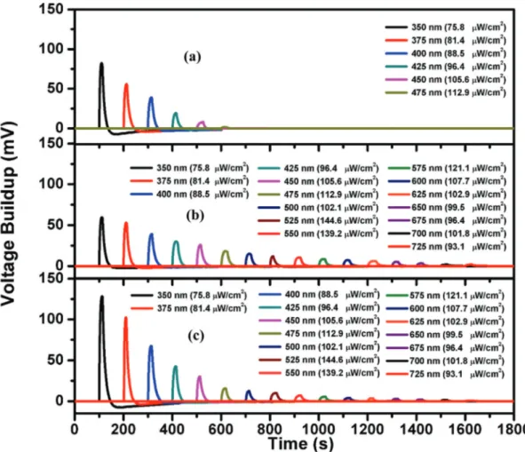
Under light illumination, a net potential buildup is observed. This voltage buildup diminishes over time after reaching the peak point, as shown in Fig. 2. We observe that capacitive charges across the Al electrodes continuously decay with the instantaneous resistor–capacitor (RC) decay of the whole circuitry (the device + external shunt resistor). Moreover, besides the exponentially decaying charges, the external circui-try tends to neutralize the trapped charges inside the NCs. Indeed, due to the presence of the highly dielectric spacer layer, the trapped electrons remain inside the NCs for which the external circuitry is inclined to enforce charge neutrality within the device. With light impinging on the device, at the point where voltage buildup reaches its peak, all these oppos-ing components become equal and balance each other. After turning off the light at the peak point, the potential decreases and even goes to negative values due to long-lived deep-trap electrons before the device returns to its initial point.24Hence, the magnitude of the final negative voltage value is directly proportional to the positive potential buildup.
Fig. 1 (a) Photograph of a semi-transparent large-area tandem photosensitive nanocrystal skin on aflexible tape. The brackets indicate the device active area which is 1.5 cm × 1.1 cm. (b) Device schematic of the tandem photosensitive nanocrystal skin. (c) Energy level diagram showing the NC conduction band (CB), valence band (VB), and the work function (Φ) of ITO and Al. After the excitons are photogenerated in each junction [(1) and (3)], the electrons are trapped inside the NCs while the holes migrate to the Al side [(2) and (4)]. (d) Cross-section scanning electron microscopy image of the tandem photosensitive nanocrystal skin on top of the Kapton substrate.
The proposed platform demonstrates a higher sensitivity if we manage to increase the number of photogenerated electron–hole pairs. Therefore, we used an extra NC monolayer to be integrated inside the device in order to increase the photogenerated potential buildup. Consequently, we added an additional NC-based junction to significantly enhance the sen-sitivity of the device. Fig. 2c shows the photoresponse spectra of the tandem structure, under the incident light radiating from the top side. A large photovoltage buildup was detected only in the case when the light was incident from the top side due to the color filtering effect of the Kapton substrate (with a cut-off at 400 nm). In response to the excitation wavelength and illumination intensity we achieved a higher voltage buildup at shorter wavelengths. Similarly, because of the increased optical absorption at shorter excitation wavelengths, which increases the number of trapped electrons inside the NCs, we observed a higher negative voltage after switching off the light. As a result of increased charging of the NCs by the trapped electrons at shorter excitation wavelengths, a longer period of time is required to recover.
We also constructed control devices to elucidate the benefits of the tandem PNS. The performance of the best
control devices is depicted in Fig. 2a and b. The tandem PNS device achieves a total photovoltage buildup at each measured optical wavelength almost equal to the sum of the photo-voltage buildup of the individual single junctions at each measured optical wavelength. We attribute the observed small difference to the mismatch between the interface layers in the tandem PNS and the fraction of the incident photons absorbed by the layers between these NC layers. To confirm the reprodu-cibility of the results obtained, 20 samples were prepared and tested, with the best device demonstrating a photovoltage buildup of 128.4 mV for an excitation intensity of 75.8 μW cm−2at 350 nm. In the course of these studies, we fabricated 11 devices with a photovoltage buildup greater than 120 mV at the impinging optical intensity of 75.8μW cm−2at 350 nm.
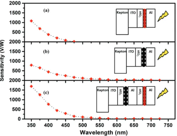
To figure out the sensitivity of the PNS, a meaningful figure-of-merit was defined according to the ratio of S = V/W, where V is the photovoltage buildup used as the readout signal and W is the incident optical power impinging on the device. Fig. 3 demonstrates the corresponding sensitivity curves as a function of the excitation wavelength.
It should be noted that the detection sensitivity remains low in the long wavelength region where the NCs exhibit poor Fig. 2 Photovoltage buildup at different excitation wavelengths and optical intensities for (a) CdTe NC-based PNS, (b) CdHgTe NC-based PNS, and (c) tandem CdTe-CdHgTe NC-based PNS. CdTe NC-based PNS exhibits no sensing after 475 nm wavelength due to the low absorption of the CdTe NC monolayer at longer wavelengths.
Paper Nanoscale
Published on 30 September 2015. Downloaded by Bilkent University on 12/23/2018 10:45:41 AM.
optical absorption. Essentially, this is because there are fewer electron and hole states available in a NC at a lower photon energy. This behavior indicates the wavelength dependence of the tandem PNS and is in strong agreement with the spectral profile of optical absorption of the NCs (see ESI-1 and 4†). Moreover, the internal quantum efficiency was measured at room temperature and no external bias was applied across the device and the samples were illuminated under a xenon light source with an integrated monochromator (see ESI-10†).
The benefit of introducing a flexible tandem PNS is twofold. It is expected to observe a sensitivity enhancement when we adapt the two separated junctions incorporated into one structure. Furthermore, unlike the conventional multi-junction devices for which the current-matching between the junctions is essential, there is no such limitation in tandem PNS devices. The photogenerated holes from an adjacent monolayer are accumulated at the top electrode, contributing their potential buildup to the overall device response. The tandem PNS is measured to exhibit a normalized detectivity of D* of 1.2 × 10⁶ Jones at 350 nm at room temperature. This level of detectivity is achieved using a single NC layer in each junction. The tandem PNS exhibits reasonably high photo-sensitivity in comparison to typical NC-based photodetectors. We measured the minimum noise equivalent intensity to be
0.34 mW cm−2, which is comparable to the solution-cast NC photodetectors reported previously.25,26 Furthermore, in the case of the tandem PNS, by decreasing the shunt resistance (e.g., from 200 MΩ to 50 MΩ, 1000 KΩ, and 200 KΩ), it is possible to speed up the response time (from 10.1 s to 2.8 s, 260 ms, and 100 ms, respectively) for an excitation intensity of 75.8 mW cm−2, comparable to the previously reported photo-detectors.27,28 The 3 dB bandwidth increases from ∼4 Hz to ∼6 Hz and ∼10 Hz when the shunt resistance is decreased from 1 MΩ to 500 KΩ and 200 KΩ, respectively. As can be seen from Fig. 4a, the increasing shunt resistance would in fact enhance the voltage buildup (sensitivity) but this would come at the cost of decreasing the 3 dB bandwidth. Therefore, the 3 dB bandwidth of the tandem PNS needs to be adjusted in regard to the requirements of a specific application.
In order to provide further electrical characterization of the tandem PNS, we measured the photovoltage buildup as a func-tion of the incident optical power. Fig. 4b shows good linearity of the tandem PNS response at different illumination intensity levels. Furthermore, the J–V characteristics under the dark con-ditions are given in ESI-11.† Very low dark current densities indicate that the dielectric layers made of a 50 nm HfO2 film
and four bilayers of PDDA-PSS block electrons and prevent them from passing through the device.
Fig. 3 A comparison of the corresponding sensitivities as a function of the excitation wavelength for (a) CdTe NC only, (b) CdHgTe NC only, and (c) tandem CdTe-CdHgTe NC PNS. The insets present the device schematics and the direction of the incident light.
In addition, tandem PNS constructed on a Kapton substrate can be cut with scissors without damaging or loss in the total sensitivity. Fig. 5a shows the tandem PNS cut into the desired geometries of arbitrary shapes. The optical performances of the cut parts are lower than that of the initial structure as expected from the dependence of the photovoltage buildup on the size of the active area. However, by summing the photo-voltage buildup of the fragments, a similar total value is obtained as the initial structure, as shown in Fig. 5b. As a con-sequence, a large-area device can be fabricated and then cut into desired smaller pieces of any shape, as long as the bottom and top contacts are intact for the electrical connections.
The radius of curvature of a bent tandem PNS was defined as the maximum bending curvature that the device can toler-ate. In the bending test, the sample was flexed with a desig-nated critical radius of curvature (Rc) during its simultaneous
characterization (see Fig. 6a and ESI-12†). The corresponding Rcvalue was measured to be 3.5 mm. Furthermore, the device
was subjected to consecutive flexing cycles at 7.5 mm radius, see Fig. 6b.
These tests show an excellent device performance, indicat-ing that flexible tandem PNS is robust under mechanical deformation, which is highly desirable for applications that require flexibility.
3.
Conclusion
In conclusion, we showed the first highly sensitive tandem PNS through the incorporation of monolayers of CdTe and CdHgTe NCs on a platform, which is also flexible, fragmenta-ble and semi-transparent. By taking advantage of an additional Fig. 4 (a) Modulation frequency response of the tandem PNS using different shunt resistors, all at a impinging optical intensity of 75.8 μW cm−2at 350 nm. The 3 dB bandwidth decreases from∼10 Hz (black) to ∼6 Hz (red) and ∼4 Hz (green) when the shunt resistance is increased from 200 KΩ to 500 KΩ and to 1 MΩ, respectively. (b) Photovoltage buildup as a function of the incident power at 425 nm wavelength.
Fig. 5 (a) The tandem PNS based on theflexible Kapton substrate cut with scissors. The device can be designed to be cut into the desired smaller pieces of any arbitrary shape. (b) The sum of the photovoltage buildups from the cut parts making up the entire device yields a similar level as in the initial uncut device for 75.8μW cm−2at 350 nm.
Paper Nanoscale
Published on 30 September 2015. Downloaded by Bilkent University on 12/23/2018 10:45:41 AM.
NC-based junction, a substantial enhancement in sensitivity and a remarked extension in the operational wavelength range were observed. The present tandem PNS was fabricated over large-areas on flexible plastics and can be used to build photo-sensitive devices with three or more junctions. Such multi-junction devices provide a route to enhance the sensitivity of PNS. These results carry potential for transparent thin-film colloidal optoelectronic devices for smart phones, smart windows and facades.
4.
Experimental section
Synthesis of nanocrystals
All the chemicals used were of analytical grade or of the highest purity available. All the solutions were prepared using Milli-Q water (Millipore) as a solvent. Al2Te3 (Cerac Inc.) was
employed for the generation of H2Te. The aqueous CdTe NCs
were synthesized as follows: 4.59 g of Cd(ClO4)2·6H2O and
1.33 g of TGA were dissolved in 500 mL of Milli-Q water. The pH of the resulting mixture was adjusted to 12 by the addition of 1 M NaOH solution and the solution was deaerated by bub-bling with argon for 30–60 min. Afterwards, under vigorous stirring, H2Te gas, generated by the reaction of 0.8 g of Al2Te3
with an excess of 0.5 M H2SO4solution, was injected into the
deaerated reaction mixture with a slow argon flow. Nucleation and growth of the NCs proceeded upon reflux of the reaction mixture under open-air conditions for 6 h. CdxHg1−xTe NCs
were synthesized employing a similar procedure according to a previously reported method.18 Briefly, 0.545 g of Cd(ClO4)2·6H2O, 0.0135 g of Hg(ClO4)2·6H2O and 0.183 g of
MPA were dissolved in 60 mL of water, followed by addition of 1 M NaOH solution up to pH = 12. 0.15 g of Al2Te3was used to
generate H2Te gas. Therefore, the molar ratio of Cd2+/Hg2+/
Te2−/MPA was 0.98/0.02/0.75/1.3. After injection of H2Te the
color of the solution turned brown. As in the case of CdTe NCs, nucleation and growth of CdxHg1−xTe NCs proceeded
upon reflux of the reaction mixture under open-air conditions for 40 min. After cooling the NC solutions to room tempera-ture, they were concentrated on a rotor evaporator by vaporiza-tion of∼90% of water. Afterwards, the NCs were precipitated by addition of 2–3 mL of isopropanol to concentrated CdTe and CdxHg1−xTe NC colloids, with their subsequent
centrifu-gation, and then redissolved in 5–10 mL of Milli-Q water. Layer-by-layer assembly
To prepare a uniform film with sufficient surface coverage for depositing the NC monolayer, we used four bilayers of PDDA-PSS. The concentrations of PDDA and PSS were 2 mg mL−1 in 0.1 M NaCl. We removed the ligands partially by adding isopropanol to the NC solutions and centrifuging the mixtures three times. To make film deposition via layer-by-layer assembly, a fully computerized dip-coater system was used. The PDDA-PSS bilayer was self-assembled by sequentially dipping a substrate into the prepared solution for 5 min and rinsed with Milli-Q water for 1 min. The thickness of the PDDA-PSS bilayer is approximately 1.4 nm as verified by the optical ellipsometry measurement. After coating one extra layer of positively charged PDDA on top of alternating bilayers, negatively-charged water-soluble NCs were coated by immer-sing the substrate for 20 min in the 4μM NC dispersion, with subsequent washing with Milli-Q water for 1 min to remove unbound NCs.
Device characterization
Photovoltage buildup characteristics of photosensitive nano-crystal skins were measured using an Agilent Technologies B1500A semiconductor parameter analyzer under a xenon light source with an integrated monochromator. The light intensity was recorded using an optical power meter (Newport multi-function optical power meter). In order to prevent the mixing of the second harmonic coming from xenon light, for the wavelengths longer than 600 nm, a color glass filter (with a cut-off of 400 nm) FSQ-GG 400 Newport was used. Fig. 6 (a) Sensitivity as a function of the radius of curvature. Theflexible PNS can be bent over 3.5 mm radius of curvature with device performance degradation to the half of the unbent configuration. (b) Performance characteristics of the device (sensitivity and photovoltage buildup) as a function of theflexing cycle.
In operation, the devices were connected to a shunt resistor (for example, 200 MΩ, or other values of choice), and no exter-nal bias was applied across the device. Due to the RC decay dependency of the devices, we adjust shunt resistances in a manner in which all RC kinetics of devices are identical. The surface sheet resistance of ITO coated Kapton was measured using the four point probe method with 40Ω sq−1. The active area is 1.5 cm × 1.1 cm, which is defined by the overlap between the bottom electrode on the Kapton substrate and the top electrode on NCs. The cross-sectional scanning electron microscopy images were obtained using a JEOL JIB-4501 multi beam focused ion beam-scanning electron microscope (FIB-SEM) at a tilted angle of 53 degrees after ion milling the device. Ion milling is performed with a protective platinum layer deposited with electron and ion beams, respectively. Reflection and transmission measurements
Reflection and transmission measurements of the devices were performed on a glass slide for stability, which is also taken as a reference for the measurements. Reflection was measured in normal incidence illumination mode using a Y-coupled fiber. The devices were illuminated with a deuter-ium/tungsten halogen light source from Semiconsoft and the reflected light was collected by using a Maya 2000 spectro-meter from Ocean optics. During the transmission measure-ments, the device was placed between two opposing fibers: one as an illumination fiber and the other one as a collection fiber. In all the measurements, the effect of the glass slide was ignored and the spectra were smoothed to avoid cavity oscil-lations of the 35μm thick Kapton substrate.
Acknowledgements
This research was financially supported by the Institute of Materials Science and Nanotechnology at Bilkent University and Nanyang Technological University. The authors are grate-ful to Mr Cuneyt Eroglu and Mr Emre Unal for the preparation of a mechanical bending instrument. The authors thank Mr Mustafa Guler for high resolution TEM imaging. HVD gratefully acknowledges the financial support in part by ESF EURYI, EU FP7 NoE Nanophotonics for Energy Efficiency, and TUBITAK under the Project no. EEEAG 110E217, 111E186, and 112E183 and in part by NRF-CRP6-2010-02 and NRF RF 2009-09. HVD acknowledges additional support from TUBA-GEBIP.
Notes and references
1 S. V. Gaponenko, Introduction to Nanophotonics, Cambridge University Press, Cambridge, UK, 2010.
2 G. Konstantatos and E. H. Sargent, Nat. Nanotechnol., 2010, 5, 391.
3 G. Konstantatos and E. H. Sargent, Appl. Phys. Lett., 2007, 91, 173505.
4 B. N. Pal, I. Robel, A. Mohite, R. Laocharoensuk, D. J. Werder and V. I. Klimov, Adv. Funct. Mater., 2012, 22, 1741.
5 F. Prins, M. Buscema, J. S. Seldenthuis, S. Etaki, G. Buchs, M. Barkelid, V. Zwiller, Y. Gao, A. J. Houtepen, L. D. A. Siebbeles and H. S. J. van der Zant, Nano Lett., 2012, 12, 5740.
6 G. Konstantatos, I. Howard, A. Fischer, S. Hoogland, J. Clifford, E. Klem, L. Levina and E. H. Sargent, Nature, 2006, 442, 180.
7 M. Razeghi, K. von Klitzing and L. Esaki, The Wonder of Nanotechnology: Quantum Optoelectronic Devices and Applications, Society of Photo-Optical Instrumentation Engineers, Washington, USA, 2013.
8 J. M. Luther, M. Law, M. C. Beard, Q. Song, M. O. Reese, R. J. Ellingson and A. J. Nozik, Nano Lett., 2008, 8, 3488.
9 A. G. Pattantyus-Abraham, I. J. Kramer, A. R. Barkhouse, X. Wang, G. Konstantatos, R. Debnath, L. Levina, I. Raabe, M. K. Nazeeruddin, M. Grätzel and E. H. Sargent, ACS Nano, 2010, 4, 3374.
10 S. Akhavan, B. Guzelturk, V. K. Sharma and H. V. Demir, Opt. Express, 2012, 20, 25255.
11 E. L. Dereniak and G. D. Boreman, Infrared Detectors and Systems, Wiley & Sons, New York, USA, 1996.
12 S. Akhavan, A. F. Cihan, B. Bozok and H. V. Demir, Small, 2014, 10, 2470.
13 S. Akhavan, K. Gungor, E. Mutlugun and H. V. Demir, Nanotechnology, 2013, 24, 155201.
14 N. Gaponik, J. Mater. Chem., 2010, 20, 5174.
15 Y. W. Lin, W. L. Tseng and H. T. Chang, Adv. Mater., 2006, 18, 1381.
16 J. W. Ostrander, A. A. Mamedov and N. A. Kotov, J. Am. Chem. Soc., 2001, 123, 1101–1110.
17 A. L. Rogach, T. Franzl, T. A. Klar, J. Feldmann, N. Gaponik, V. Lesnyak, A. Shavel, A. Eychmüller, Y. P. Rakovich and J. F. Donegan, J. Phys. Chem. C, 2007, 111, 14628.
18 V. Lesnyak, A. Lutich, N. Gaponik, M. Grabolle, A. Plotnikov, U. Resch-Genger and A. Eychmüller, J. Mater. Chem., 2009, 19, 9147.
19 V. Lesnyak, N. Gaponik and A. Eychmüller, Chem. Soc. Rev., 2013, 42, 2905.
20 C. B. Murray, D. J. Norris and M. G. Bawendi, J. Am. Chem. Soc., 1993, 115, 8706.
21 G. Konstantatos, I. Howard, A. Fischer, S. Hoogland, J. Clifford, E. Klem, L. Levina and E. H. Sargent, Nature, 2006, 442, 180.
22 J. Jasieniak, M. Califano and S. E. Watkins, ACS Nano, 2011, 5, 5888.
23 A. L. Rogach, N. Gaponik, J. M. Lupton, C. Bertoni, D. E. Gallardo, S. Dunn, N. Li Pira, M. Paderi, P. Repetto, S. G. Romanov, C. O’Dwyer, C. M. Sotomayor Torres and A. Eychmüller, Angew. Chem., Int. Ed., 2008, 47, 6538. 24 P. O. Anikeeva, C. F. Madigan, J. E. Halpert, M. G. Bawendi
and V. Bulović, Phys. Rev. B: Condens. Matter, 2008, 78, 085434.
Paper Nanoscale
Published on 30 September 2015. Downloaded by Bilkent University on 12/23/2018 10:45:41 AM.
25 D. C. Oertel, M. G. Bawendi, A. C. Arango and V. Bulović, Appl. Phys. Lett., 2005, 87, 213505.
26 Y. Jin, J. Wang, B. Sun, J. C. Blakesley and N. C. Greenham, Nano Lett., 2008, 8, 1649.
27 Y. R. Tao, X. C. Wu and W. W. Xiong, Small, 2014, 10, 4905.
28 Y. R. Tao, X. C. Wu, W. Wang and J. N. Wang, J. Mater. Chem. C, 2015, 3, 1347.