Lateral and Vertical Heterostructures of h
‑GaN/h-AlN: Electron
Con
finement, Band Lineup, and Quantum Structures
A. Onen,
†D. Kecik,
†E. Durgun,
*
,†and S. Ciraci
*
,‡†UNAM-Institute of Materials Science and Nanotechnology, Bilkent University, Ankara 06800, Turkey ‡Department of Physics, Bilkent University, 06800 Ankara, Turkey
ABSTRACT: Lateral and vertical heterostructures constructed of two-dimensional (2D) single-layer h-GaN and h-AlN display novel electronic and optical properties and diverse quantum structures to be utilized in 2D device applications. Lateral heterostructures formed by periodically repeating narrow h-GaN and h-AlN stripes, which are joined commensurately along their armchair edges, behave as composite semiconducting materials. Direct−indirect characters of the fundamental band gaps and their values vary with the widths of these stripes. However, for relatively wider stripes, electronic states are confined in different stripes and make a semiconductor−semiconductor junction with normal band alignment. This way one-dimensinonal multiple quantum well
structures can be generated with electrons and holes confined to h-GaN stripes. Vertical heterostructures formed by thin stacks of h-GaN and h-AlN are composite semiconductors with a tunable fundamental band gap. However, depending on the stacking sequence and number of constituent sheets in the stacks, the vertical heterostructure can transform into a junction, which displays staggered band alignment with electrons and holes separated in different stacks. The weak bonds between the cations and anions in adjacent layers distinguish these heterostructures from those fabricated using thinfilms of GaN and AlN thin films in wurtzite structure, as well as from van der Waals solids. Despite the complexities due to confinement effects and charge transfer across the interface, the band diagram of the heterostructures in the direct space and band lineup are conveniently revealed from the electronic structure projected to the atoms or layers. Prominent features in the optical spectra of the lateral composite structures are observed within the limits of those of 2D parent constituents; however, significant deviations from pristine 2D constituents are observed for vertical heterostructures. Important dimensionality effects are revealed in the lateral and vertical heterostructures.
■
INTRODUCTIONSoon after the synthesis of graphene,1similar single-layer (SL) hexagonal structures, h-GaN and h-AlN, were predicted for III−V nitride compounds.2 Later, the stability of these and other similar compounds were confirmed based on extensive analysis of phonon dispersions3and, recently, on ab initiofinite temperature molecular dynamics calculations.4,5 Following the predictions of these SL structures, several theoretical studies have been carried out4−18 with the premise of attaining extraordinary optoelectronic properties of 3D wurtzite GaN and AlN (wz-GaN and wz-AlN)19−25in 2D SL and multilayers (ML).
After the epitaxial growth of ultrathin h-AlN on single crystal Ag(111)26and the synthesis of 2D GaN on SiC(0001) through graphene encapsulation,27 2D h-AlN and h-GaN have been activefields of research. The prime motivation underlying these diverse research works has been to utilize the electronic properties of these SL and ML structures in 2D electronics. Recently, efforts in designing novel electronic materials went far beyond tuning the electronic structure by stacking single layers vertically. In fact, previous theoretical works on the junctions of
SL nanoribbons of h-GaN/h-AlN,3 graphene/h-BN
hetero-structures,28 and even graphene nanoribbons with graded widths29 predicted one-dimensional (1D) multiple quantum well structures with well-defined band lineups and confine-ments of carriers. Recent experimental studies fabricating BN/ graphene30and WS2/MoS231 in-plane lateral heterostructures have motivated the construction of composite materials. Not only lateral heterostructures but also heterostructures made from vertically stacked SL materials have been considered.32 More recently, unusual features of in-plane (graphene)/(BN), metal/insulator composite structures,33 and graphene/BN/ graphene vertical and in-plane nanocapacitors,34,35 Schottky barriers and spin-valves constructed of the lateral hetero-structures of transition metal dichalcogenides36 have been proposed.
In this paper, we take an important step forward toward developing novel composite nanomaterials from SL h-GaN and h-AlN. We first investigate the periodic, in-plane, lateral heterostructures constructed of h-GaN and h-AlN stripes of
Received: August 21, 2017
Revised: October 29, 2017
Published: November 21, 2017
different widths, which join commensurately along their armchair edges. These heterostructures are specified as A:(h-GaN)p/(h-AlN)q with p and q being formula units of the constituents in the unit cell. In these heterostructures, the interface or boundary between adjacent constituents is 1D and their coupling is rather strong. As an alternative to the lateral composite structures, we also investigate vertical heterostruc-tures, V:(h-GaN)m/(h-AlN)n composed of m 2D SL h-GaN and n h-AlN sheets, which are vertically and commensurately stacked. The atomistic models of both types of heterostructures discussed in this study are presented inFigure 1a,b.
Earlier, it has been demonstrated that stable bilayers (BL) and multilayers (ML), even 3D layered structures, can be constructed of the stacks of SL h-GaN and h-AlN constituents in specific stacking geometries.4,5In this study we carried out an analysis revealing that vertical heterostructures correspond to local minima, where they are prevented from transitions to lower energy structures in global minimum. Even if the interlayer interaction in these vertical heterostructures composed of attractive van der Waals (vdW) and also weak chemical interactions is slightly stronger than that in pure vdW solids, it is, however, weaker than the bonds in 3D wz-GaN and wz-AlN. In this respect, vertical heterostuctures studied in this work are distinguished from the heterostructures fabricated for
two decades from thin films of wz-GaN and wz-AlN by
molecular beam epitaxy (MBE) or metal−organic chemical vapor deposition (MOCVD) methods. The vertical hetero-structures here differ also from pure vdW heterostructures such as WS2/MoS2. Hence, the present study brings the differences among those heterostructures into focus and hence introduces a new class of electronic nanostructure. Particularly, band lineup characterizing a heterostructure exhibits a crucial dimensionality effect in the lateral and vertical heterostructures. It is also shown that the optical properties attained in lateral and vertical heterostructures here are rather different from their SL parent constituents.
■
COMPUTATIONAL METHODWe carried out spin polarized density functional theory (DFT) calculations to determine the ground-state total energy and electronic structure of lateral and vertical heterostructures. Projector-augmented-wave potentials (PAW) formalism37 as implemented in the Vienna ab initio simulation package
(VASP)38,39was used. The electron exchange and correlation (XC) potential is described by the generalized gradient approximation (GGA) with d electrons also taken into account (GGA-d XC potential),40within the Perdew−Burke−Ernzerhof (PBE) form. An exception to using the standard PBE XC functional has been for the total and Bader charge density calculations of Al atom, since it was necessary to include the contribution of 2s 2p orbitals to the ground-state charge. The plane-wave basis set was taken as an energy cutoff of 520 eV for all calculations. The vdW interactions were also considered for heterostructure systems treated in this paper.41 The supercell method was undertaken in order to treat periodic, lateral, and finite size, vertical heterostructures. We used the conjugate gradient method for optimizing the atomic positions, interlayer spacings, and lattice constants. To this end, the total energy and
atomic forces were minimized with an energy difference
between the sequential steps set to 10−5eV for convergence. The maximum allowed force on each atom and Gaussian smearing factor were taken as 0.02 eV/Å and 0.05 eV, respectively. As for the Brillouin zone (BZ) sampling,42 Γ-centered 27× 27× 1 (24× 24× 1) k-grid was undertaken for the periodic armchair-edged lateral (finite vertical) heterostructure A:(h-GaN)p/(h-AlN)q [V:(h-GaN)m/(h-AlN)n] with p/q = 2 (m/n = 1) and scaled accordingly for larger systems. In order to avoid the spurious interactions between the periodic images, a supercell with∼15 Å vacuum space was adopted for the lateral heterostructures. The interatomic charge transfer between Ga− N and Al−N pairs (bonds) was carried out for the armchair p = 16 and q = 16 heterostructures, using the Bader charge analysis method, by increasing the criterion for the precision of the calculations.43
The energetics of heterostructures are characterized by their cohesive energy, formation energy, and junction energy as defined in ref 4. In particular, the average junction energy relative to 2D SL structures defined as E̅j[p/q] = pET[h-GaN] + qET[h-AlN]− ET[A:(h-GaN)p/(h-AlN)q] is calculated in terms of the total energies of 2D SL GaN (per formula unit), h-AlN, and lateral heterostructure A:(h-GaN)p/(h-AlN)q. Accord-ing to this definition, E̅j > 0 favors the junction formation. Despite small negative values of E̅j, a heterostructure is formed from stripes, since the energy is gained through the saturation of the dangling bonds at the armchair edge. The composite structures treated in this study have positive cohesive energy but small negative formation energy relative to the parent 3D
Figure 1.(a) Atomistic model of lateral and periodic heterostructure, A:(h-GaN)p/(h-AlN)qwith p = 16 and q = 16 being formula units of constituents in the unit cell. Asymmetric boundaries between h-GaN and h-AlN stripes along their armchair edges are I1and I2. Ga, Al, and N atoms are represented by large blue, large red, and small gray balls, respectively. Lateral heterostructure is in thexy plane. (b) Same forfinite size (single), vertical heterostructures, V:(h-GaN)m/(h-AlN)nwith m = 7 andn = 7 being the numbers of the constituent sheets in the stack. Constituent sheets of vertical heterostructure are in the xy plane; the heterostructure extends along thez axis. A cation (anion) in any layer is directly below and above the anion (cation) in the adjacent layers.
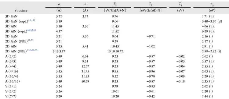
Table 1. Energetics Related with 3D wz-GaN, wz-AlN, 2D SL h-GaN, h-AlN, A:(h-GaN)p/(h-AlN)q, and V:(h-GaN)m/(h-AlN)na
a b E̅c E̅f E̅j Eg
structure (Å) (Å) [eV/Ga(Al)-N] [eV/Ga(Al)-N] (eV) (eV)
3D GaN 3.22 3.22 8.76 1.71 (d)
3D GaN (expt.)44−49 3.19 9.06 3.40−3.50 (d)
3D AlN 3.30 3.30 11.45 4.06 (d)
3D AlN (expt.)46,50,51 4.37 11.52 6.28 (d)
2D GaN 3.21 5.56 8.04 −0.71 2.16 (i)
2D GaN (PBE)52,53 3.21 8.38 2.17 (i)
2D AlN 3.13 5.41 10.43 −1.02 2.91 (i)
2D AlN (PBE)5,15,54,55 3.13,3.17 10.10,10.72 2.88−2.92 (i)
A:(2/2) 5.49 6.34 9.23 −0.87 −0.02 2.62 (i) A:(3/3) 5.49 9.51 9.23 −0.87 −0.03 2.57 (d) A:(4/4) 5.49 12.67 9.23 −0.87 −0.04 2.55 (i) A:(4/16) 5.45 31.45 9.95 −0.96 −0.07 2.63 (d) A:(16/4) 5.53 31.93 8.52 −0.78 −0.08 2.29 (d) A:(16/16) 5.49 50.69 9.23 −0.87 −0.18 2.35 (d) V:(1/1) 3.24 9.79 −0.83 2.62 (i) V:(2/2) 3.26 10.01 −0.61 2.20 (i) V:(7/7) 3.29 10.20 −0.42 1.44 (i)
aLattice constants a andb; average cohesive energy, E̅
c; formation energy, E̅f; junction energy, E̅j; fundamental band gap, Eg(d, direct or i, indirect).
Figure 2.Energy band structure of A:(h-GaN)p/(h-AlN)qlateral heterostructure along symmetry directions of rectangular BZ. (a) p/q = 2/2. (b) p/ q = 3/3. (c) p/q = 4/4. Unit cells and the Brillouin zones are also shown. Eg−dand Eg−iindicate direct and indirect band gaps, respectively. (d) Variation of the fundamental (smallest) band gap, with p = q or width (w) of the GaN side.
wz-GaN and wz-AlN; hence, heterostructures are energetically unfavorable relative to their 3D parent crystals. Under these circumstances, the important questions are whether the composite structures treated in this study are stable dynamically and whether they sustain high-temperature thermal excitations. Since the dynamical and thermal stabilities of the hetero-structures were proven in our earlier works, we will not treat them here. InTable 1, the calculated values of lattice constants, cohesive, formation and junction energies, and fundamental band gap of heterostructures are presented. For the sake of comparison, calculated values of 3D wz-GaN, wz-AlN, 2D h-GaN, and h-AlN together with available experimental and theoretical values are also given.
Random phase approximation (RPA)56−58 is employed on top of the PBE approach, in order to obtain the optical spectra, using a sufficient number of (valence and conduction) bands ranging between 96 and 320 for all types of heterostructures considered in this study. Monkhorst−Pack42k-point sampling adopted for PBE-RPA calculations of the armchair-edged lateral (p/q = 1) and vertical (m/n = 1) heterostructures was 37× 37 × 1, which is down scaled accordingly for larger systems.
■
ARMCHAIR EDGED LATERALHETEROSTRUCTURES
Among the lateral heterostructures, wefirst consider the ones having small p = q and calculate the electronic band structures of the optimized A:(h-GaN)p/(h-AlN)qstructures for p/q = 2/ 2, 3/3, and 4/4. InFigure 2, the energy bands of these lateral heterostructures are presented.
While 2D SL h-GaN and h-AlN are wide band gap semiconductors with fundamental PBE indirect band gap of
Eg−i = 2.16 and 2.91 eV, respectively, three periodic
heterostructures inFigure 2display electronic structures rather different from their parent 2D constituents, as well as from each other. The first one, A:(h-GaN)2/(h-AlN)2, is a composite structure constructed of very narrow stripes and is a semiconductor with an indirect band gap of 2.62 eV, which is wider than the average band gap of its constituents. Its large direct band gap of 2.90 eV occurs at the center of the BZ. The second heterostructure, A:(h-GaN)3/(h-AlN)3, displays an electronic structure which is different from the first one. It has a slightly smaller but direct band gap. In the third one, A: (h-GaN)4/(h-AlN)4, which is constructed of slightly larger stripes relative to the formers, the band gap becomes indirect again. In this last heterostructure, the electronic states start to confine in different constituent stripes. These changes in the electronic structure as p = q increases from 2 to 4 clearly indicate the importance of the in-plane, lateral composite structures in modifying and tuning the properties of SL h-GaN and h-AlN in order to design new 2D materials. To deduce the variation of the fundamental band gap [smallest (direct or indirect) band gap] with p = q, we calculated the band structures of A:(h-GaN)p/(h-AlN)q for 2≤ (p = q) ≤ 24 and present it inFigure 2d. Accordingly, as p = q→ ∞, the smallest band gap Eg→ 2.16 eV, the band gap of 2D SL h-GaN. Due to the confinement effect discussed in the next section, the smaller the width (w) of the h-GaN stripe, the larger the band gap is. Another way of tuning the properties of parent constituent single layers can be achieved through the δ-doping, whereby one chooses small p, but large q, or vice versa, such as A:(h-GaN)4/(h-AlN)16 or A:(h-GaN)16/(h-AlN)4, as shown in Figure 3. This is reminiscent of the situation where a row of atoms in a 2D structure is substituted by different types of
atoms. This way, a narrow 1D stripe of different electronic properties is implemented in a wide and different stripe, so that the electronic structure at the close proximity of the dopant row is modified. InFigure 3a, a wide h-AlN stripeδ-doped by a narrow h-GaN stripe is repeated periodically. Hence, a 1D semiconductor of smaller band gap is attained in a semi-conductor h-AlN, which has a relatively wider band gap. In the momentum space, the direct band gap of 2.63 eV at the center of BZ is derived from the narrow h-GaN stripe. Accordingly, a wide 2D h-AlN with a band gap of 2.91 eV attains a 1D character with the band gap of 2.63 eV. Conversely, inFigure 3b, the wide, SL h-GaN with band gap of 2.16 eV is periodically δ-doped by a narrow, h-AlN stripe to form a new composite material, in which a narrow 1D rod has a relatively wider band gap. Eventually, the fundamental gap raises to 2.29 eV. The situation seen inFigure 3reveals a new path to functionalize a 2D material for complex and directional device operations. We note also the possibility ofδ-doping of SL h-GaN and h-AlN by nearly lattice matched, narrow SiC and BP to attain even more interesting electronic structures.
1D Multiple Quantum Well Structure. Next we study lateral heterostructures having both constituent ribbons wide enough to allow the electronic states to confine in either constituent stripes. We consider the heterostructure A:(h-GaN)16/(h-AlN)16 and calculate its energy band structure, crystal potential, density of states, and charge density projected
Figure 3.Electronic band structure and unit cells of heterostructures constructed by implementing the narrow stripe of one constituent into the other wide constituent, leading to a periodicδ-doping. (a) A:(h-GaN)4/(h-AlN)16and (b) A:(h-GaN)16/(h-AlN)4.
at Ga−N and Al−N bonds (i.e., constituent cation−anion pairs) located at different places. In Figure 4a, we show the atomic configuration in the unit cell. The stripes extend along x direction parallel to the armchair edges and heterostructure repeats periodically along the y axis. As we demonstrate in Figure 5, the electronic states are confined to the constituent stripes and approximate to their 2D parent crystals. Thus, initially a unique 2D semiconductor with small p and q transforms into ribbons of its constituents. Confinement takes place when a state of one stripe cannotfind a matching partner in the adjacent stripe with the same energy and momentum. The states are confined if the band gap of the adjacent stripe poses an energy barrier.
InFigure 4b, we present the isosurfaces of total charge and the net charge on each cation and anion in the unit cell. While inside the GaN stripe,∼1.5 electrons are donated to N atom, and ∼2.5 electrons are transferred from Al to N in the AlN stripe. At the boundary region, charge on the cation and anion makes a smooth transition. InFigure 4c, the xz plane averaged electronic potential energy and its average value V̅(y) are shown. Notably, V̅(y) is neither flat nor tilted due to the charge transfer between the stripes; rather it is curved with aflat region
in the GaN stripe. It is however noted that theflat region can appear inside the stripes when p and q are large.
InFigure 4d, the band diagram in the direct space is shown in terms of the variation of the valence band edge, EVB(y), and conduction band edge, ECB(y). These band edges are retrieved directly from the total state densities projected to each cation (Ga or Al)−anion (N) pairs in different locations. The energy band diagram displays a normal band lineup with quantum wells for electrons and holes occurring in the h-GaN stripe. Other interesting features one realizes are as follows: (i) Band edges areflat but change smoothly as one goes from the h-GaN stripe to the adjacent h-AlN stripe. (ii) The variations of the band edges at the interface are not sharp; they vary smoothly as they join from one stripe to the other at distance, l < 2a. (iii) The band gap in the h-GaN stripe is wider than that of the parent 2D h-GaN. It is, however, narrower in the h-AlN stripe as compared to the parent 2D h-AlN. Namely, while 2D h-GaN has a band gap of 2.16 eV, the gap at the center of the h-GaN stripe of the heterostructure is 2.35 eV. In contrast, the band gap at the center of the AlN stripe is 2.78 eV, which is 0.13 eV smaller than that of the parent 2D h-AlN. This is explained in terms of the confinement effect, where carriers confined in the quantum wells in the h-GaN stripe of width (w) set the highest
Figure 4.Periodically repeating A:(h-GaN)16/(h-AlN)16 heterostructure. (a) Atomic configuration in the unit cell. Stripes extend along the x direction. The y axis is perpendicular to the armchair edges and to the boundaries. (b) Charge density isosurfaces and effective charge on the cation and anion atoms in the unit cell. (c) The xz plane averaged electronic potential energy (blue lines) and its averaged value along they direction V̅(y) (red line). (d) Energy band diagram in the direct space along the y axis showing multiple quantum well structures for electrons and holes. Valence band and conduction band edges, ECBand EVB, are retrieved from the band gap of local density of states at each cation−anion pair in the unit cell and are marked with black balls joined by thick gray lines. Band edges for p =q→ ∞ are indicated by dash−dotted lines. The average potential V̅(y) is marked by red lines. Alternatively, ECBand EVB, also deduced using V̅(y) (see text), are marked by thick green lines.
valence (lowest conduction) band states at lower (higher) energies byΔEg≈ 0.1 eV. Conversely, the confinement effect works in the reverse direction for the h-AlN stripe, andΔEgis found to be∼0.06 eV. These are natural consequences of the uncertainty principles, and the confinement energy can be understood by a crude model as the ground state of a free electron (hole) in an infinite square potential well of width w, namely ΔEg = ℏ2/(8mw2). Such a crude model predicts the confinement of carriers by overestimating ΔEg as ∼0.5 eV. Accordingly, the narrower the w of the h-GaN stripe or quantum well, the largerΔEgis. The widening of the band gap is confirmed in Figure 2d showing the variation of Eg as a function of p = q.
Alternatively, the variation of the band edges, EVB(y) and ECB(y), can also be determined using the model developed for bulk heterostructures with a 2D interface.59−62To this end, one first determines V̅(y) in 2D h-GaN and h-AlN and then calculates the energies of the band edges relatively. We found EVB=−0.73 (−0.58) eV and ECB= 1.42 (2.33) eV for 2D
h-GaN (h-AlN). Normally, band edges in A:(h-h-GaN)16
/(h-AlN)16 are calculated by using these energies. First V̅(y) is transferred from the state inFigure 4, panels c to d. After the
correction of the confinement effect, the valence and
conduction band edges are deduced. Apparently, the band diagram and band alignment determined this way do not agree with those obtained directly from the electronic structure.
The electronic energy band structure of the A:(h-GaN)16 /(h-AlN)16 heterostructure in the momentum space is shown in Figure 5. The direct band gap at the center of the BZ is 2.36 eV, which corresponds to the minimum gap in the band diagram in
the direct space. The two lowest band states at the conduction band edge are confined in the h-GaN stripe behaving as a quantum well. The third conduction band state at higher energy is confined in the AlN stripe, since it cannot find any matching state in the h-GaN stripe. The fourth andfifth states are propagating throughout the heterostructure. As one goes from the top of the valence band toward lower energies,first nine states (five of which are shown in Figure 5) are also confined in the h-GaN stripe. Note that the localization of these conduction and valence band states confirm the normal band lineup.
We note that, in the direct−indirect transition of the fundamental band gaps and the variation of the electronic structure as a function of the widths of stripes, the band diagram in the direct space depends on whether the stripes are joined commensurately along zigzag or armchair edges. In this respect, armchair edged lateral heterostructures here comple-ment the earlier work on zigzag edged lateral heterostruc-tures.18 Additionally, comparison of armchair edged lateral heterostructures with vertical ones revealed interesting features.
■
FINITE SIZE VERTICAL HETEROSTRUCTURESVertical heterostructures are constructed by stacking 2D SL
h-GaN and h-AlN. Here we consider only finite size
heterostructures composed of SL h-GaN stack continued vertically by a stack of SL h-AlN, specified as V:(h-GaN)m /(h-AlN)n. By changing the number of layers m and n and/or by the order of the constituent stacks like V:(h-GaN)m/(h-AlN)n /(h-GaN)m or V:(h-AlN)n/(h-GaN)m/(h-AlN)n, one can attain diverse device characteristics. Similar heterostructure combina-tions were fabricated for two decades by depositing thinfilms of wz-GaN and wz-AlN. However, these heterostructures differ from the vertical heterostructure treated in this study with weak vdW and weak chemical interactions.
At this point we address the important question of whether vertical heterostructures constructed by stacking of SL h-GaN and h-AlN with their large interlayer spacings are stable or they transform to the more energetic, wurtzite thin films. Experi-ments synthesizing ultrathin films of AlN26 and GaN27 have found lattice constants smaller than those of AlN and wz-GaN, respectively. These experiments presented evidence that the ultrathin films can have layered hexagonal structures. We also carried out phonon calculations and ab initio molecular dynamics calculations at high temperature, which assured that BL and ML structures, even 3D layered structures constructed of SL h-GaN or h-AlN, are stable. Additionally, in order to show that vertical heterostructures by themselves remain stable in local minima without transforming to another lower energy configuration or global minimum, we carried out the following analysis. First we calculated the optimized total energy of V:(h-GaN)1/(h-AlN)1and V:(h-GaN)2/(h-AlN)2by decreasing the interlayer spacings gradually down to distances smaller than the anion−cation distance in wz structures. The total energy increased as the interlayer spacings decreased. We repeated this analysis in larger 2× 2 and 4 × 4 supercells in order to allow more freedom for a structural transformation. However, no structural transformation to a lower energy state occurred; rather layered structures with AA′ stacking were maintained. Finally, we carried out ab initio molecular dynamic calculations up to 1000 K for 4 ps in 4× 4 supercells. Even if the snapshots of atomic configurations displayed the formation of local haeckelite-like structures with relatively shorter cation−anion bonds, it was observed only temporarily. In the course of a long
Figure 5. Energy band structure and charge density isosurfaces of specific states of the A:(h-GaN)16/(h-AlN)16heterostructure. The Journal of Physical Chemistry C
simulation time at high temperatures, the layered structures were prevented to transform into lower energy wz-like configurations, but the overall layered character with large interlayer spacings was maintained.
Having demonstrated that the vertical heterostructures treated in this study are stable, we now discuss their electronic properties. InFigure 6, two vertical heterostructures with their electronic band structure and total and projected densities of states are shown. Thefirst one is actually a bilayer of single h-GaN and h-AlN. This heterobilayer displays properties different from those of 2D SL h-GaN and h-AlN, also different from the bilayers of each constituent. While the bilayers of GaN and h-AlN have indirect band gaps of 2.08 and 3.54 eV, respectively, with an average value of 2.81 eV, the band gap of the V:(h-GaN)1/(h-AlN)1 heterostructure is indirect but 2.62 eV. The photoelectric threshold ΦB = 5.05 eV and the Fermi level occurs above the maximum of electronic potential energy between h-GaN and h-AlN layers. In contrast to vdW heterostructures, this situation indicates a chemical interaction between the layers. The second heterostructure, V:(h-GaN)2/ (h-AlN)2 in Figure 6, is composed of the vertical stacks of bilayers of h-GaN and h-AlN. It has ΦB = 4.77 eV and an indirect band gap of 2.20 eV, which constitute a significant change relative to thefirst heterostructure. Here, finite size or periodic stacking sequence, m and n are parameters to attain novel composite materials with tunable electronic structure. Additionally, as the numbers of layers of the constituents at either side of the heterostructure increase, electrons start to confine at the constituent stacks. This can lead to semi-conductor/semiconductor junctions with well-defined band
alignment. Alternatively, one can construct vertical hetero-structures between h-GaN or h-AlN and lattice matched multilayers of metallic silicene or germanene forming a Schottky barrier. Here we rather concentrate on finite size semiconductor/semiconductor junctions of 2D GaN and h-AlN.
2D Quantum Well. In this section we examine the vertical heterostructures, V:(h-GaN)7/(h-AlN)7 and V:(h-AlN)4 /(h-GaN)6/(h-AlN)4. Thefirst one can be viewed as the junction of two semiconductors with different band gaps. The band diagram in the direct space inferred from the TDOS projected to each cation−anion pairs in the unit cell inFigure 7b suggests a staggered band lineup. Accordingly, the quantum well of electrons occurs in the h-GaN stack. The quantum well for holes is shallow and at h-AlN stack. In Figure 7c, the energy bands showing the contributions of specific cation−anion pairs reveal local band gaps at the cation−anion pairs indicated by arrows, which are in agreement with the band diagram in the direct space. InFigure 7d, the indirect band gap is 1.44 eV and occurs between the lowest conduction band state located in the h-GaN stack atΓ-point and highest valence band state located in h-AlN stack alongΓ-K direction. The photoelectric threshold energy is ΦB = 5.59 eV. The isosurfaces of the charges of specific band states at Γ-point are in compliance with the band diagram inFigure 7b. While the six lowest conduction band states (four of which are shown inFigure 7) are confined to the h-GaN stack, only one state at the top of the valence band is confined to the h-AlN state providing a shallow well for holes. The vertical heterostructure, V:(h-GaN)4/(h-AlN)6 /(h-GaN)4, differs by the stacking sequence as shown inFigure 8.
Figure 6. (a) V:(h-GaN)1/(h-AlN)1: Atomic configuration in the unit cell with BZ, plane averaged electronic potential energy, energy band structure, total (TDOS) and projected densities of states. (b) Same for V:(h-GaN)2/(h-AlN)2.
Two quantum wells of electrons occur at h-GaN stacks at both sides of the central h-AlN stack according to the staggered band alignment. Here the conduction band edge at the h-AlN stack becomes a barrier and the whole heterostructure can function as a resonant tunnelling device. Since the valence band edge of the AlN stack is slightly above the valence band edge of the h-GaN stack, a shallow well for a hole is formed.
■
OPTICAL PROPERTIES OF LATERAL AND VERTICAL HETEROSTRUCTURESRPA spectra of lateral armchair and vertically stacked heterostructures of h-GaN/h-AlN are plotted in Figure 9. The imaginary dielectric functions [ε2(ω)] of A:(h-GaN)2 /(h-AlN)2, A:(h-GaN)16/(h-AlN)4, and A:(h-GaN)4/(h-AlN)16 in-plane armchair heterostructures are shown in comparison to SL
Figure 7.(a) Stacking sequence offinite size vertical heterostructure, V:(h-GaN)7/(h-AlN)7. 2D h-GaN and h-AlN sheets are represented by Ga−N and Al−N pairs, respectively. Ga, Al, and N atoms are represented by large blue, large red, and small gray balls, respectively. (b) Energy band diagram in the direct space along the y axis showing multiple quantum well structures for electrons and holes. Valence band and conduction band edges, ECBand EVB, are retrieved from the band gaps of the local density of states (LDOS) at each cation−anion pair in the unit cell and are marked with black balls joined by thick gray lines. Minute LDOS in the gap are numerical artifacts of projection. (c) Energy bands in the momentum space showing the contributions of specific cation−anion pairs indicated by arrows show the maximum band gap in h-GaN and h-AlN stacks. (d) Energy bands in momentum space and (e) charge density isosurfaces showing the distribution of band states at the edges of the conduction and valence bands atΓ-point.
pristine h-GaN and h-AlN, for light polarized along x, y, and z directions, respectively inFigure 9a−d. As for the trends in the optical properties of armchair-edged lateral composite structures, a gradual blueshift of the optical absorption onsets in the range of 1.8−3.1 eV and of the absorption peaks takes place once AlN proportion is increased, for xy polarization (even though the onsets and peaks are not exactly positioned due to the band gap underestimation of PBE method, this method is sufficient for a quantitative evaluation). Considering the gradually increasing band gaps once AlN content is
increased, the aforementioned blueshifts are expected. While the spectral features and band-edge regarding the A:(h-GaN)2/ (h-AlN)2structure present a well-distributed combination of SL h-GaN and h-AlN, the δ-doped armchair-edged heterostruc-tures display optical transition feaheterostruc-tures closer to their respective pristine counterparts. The blueshifted absorption band-edges stand for the gradually increasing direct band gaps of the respective armchair heterostructures, which are 2.29, 2.63, and 2.90 eV. Beyond the onsets, main absorption peaks ranging between 5.3 and 5.9 eV originate from the predominant
Figure 8.Same asFigure 7for thefinite size vertical heterostructure, V:(h-GaN)4/(h-AlN)6/(h-GaN)4: (a) Stacking sequence offinite size vertical heterostructure V:(h-GaN)4/(h-AlN)6/(h-GaN)4. (b) Energy band diagram in the direct space along the y axis showing multiple quantum well structures for electrons and holes. (c) Energy bands in the momentum space showing the contributions of specific cation−anion pairs indicated by arrows show the maximum band gap in h-GaN and h-AlN stacks. (d) Energy bands in momentum space and (e) charge density isosurfaces showing the distribution of band states at the edges of the conduction and valence bands atΓ-point.
interband transitions between the valence and conduction bands. For the optical response polarized along z, no major differences are observed as all structures are single-layer.
Once a SL of h-AlN is stacked vertically on SL h-GaN, for polarization along the xy direction, an intriguing aspect is the optical absorption onset of the vertical heterostructure located
midway between those of SL h-GaN and h-AlN [see Figure
9b]. In compliance with its direct band gap of 3.14 eV, the absorption onset of the V:(h-GaN)1/(h-AlN)1 structure appears slightly below 3 eV. With regard to the early features in the optical spectrum, an extra shoulder peak for the vertical heterostructure is observed near 5 eV, while the major luminescence peak ranges between 6 and 8 eV and is
blueshifted by ∼2 and ∼1 eV with respect to SL GaN and
AlN, respectively. The divergences in spectral shape and absorption peak positions mainly arise from different optical transitions of which the extended interband transitions within the V:(h-GaN)1/(h-AlN)1vertical heterostructure are respon-sible. Another remarkable outcome is the intensified amplitude of the spectrum, where the absorption is preserved active until above 12 eV. Moreover, a comparison between V:(h-GaN)1/ (h-AlN)1and V:(h-GaN)2/(h-AlN)2composite structures and bilayers of h-GaN and h-AlN is given in Figure 9c, which indicates the similar gradual and uniform blueshift of the onset and overall peak features, where the spectral features and intensity of the bilayer and V:(h-GaN)1/(h-AlN)1 spectra resemble one another. On the other hand, amplitude ofε2(ω) of the V:(h-GaN)2/(h-AlN)2structure is dramatically intensi-fied, with a slightly red-shifted interband absorption edge with respect to V:(h-GaN)1/(h-AlN)1, owing to its direct band gap of 2.68 eV. Moreover, the optical activity range of its main absorption peak is drastically extended, i.e., above 5.5 eV and reaching a maximum amplitude at ∼8 eV, originating from relatively less dispersed and increased number of GaN and AlN bands and thus intensified direct optical (interband) transitions.
Finally, Figure 9e,f shows the out-of-plane optical response, where, regarding the vertical heterostructures of h-GaN/h-AlN, an improved absorption could only be observed for V:(h-GaN)2/(h-AlN)2.
In summary, regarding both armchair-edged and vertical heterostructures, differences in the optical spectral features, absorption peak positions, peak ranges, and amplitudes, with respect to their parent constituents originate from varying character and range of interband transitions, indicated by distinct GaN and AlN contributions. The blueshifted band edges and peaks of the armchair heterostructures upon increasing direct band gaps toward increasing AlN content also allows for the modulation of optical absorption, especially promising for potential device applications of 2D h-GaN/h-AlN based heterostructures within the ultraviolet regime. Finally, in-plane optical absorption can be improved by stacking at least two layers of h-AlN on double-layered h-GaN.
■
DISCUSSIONS AND CONCLUSIONSSL h-GaN and h-AlN are stable nanostructures with remarkable properties originated from 3D bulk GaN and AlN in their wurtzite structure. Both are wide band gap, nonmagnetic semiconductors. They can form also stable bilayer, trilayer, even periodic layered structures, whereby their electronic properties vary with the number of layers. In this study we demonstrated that SL h-GaN and h-AlN are combined in different ways to form heterostructures with properties different from their parent constituents. This was achieved by constructing lattice matched lateral and vertical heterostructures. These two types of heterostructures, while in the former two constituents are separated through a 1D line, and in the latter the interface is planar, showed crucial dimensionality effects.
In lateral heterostructures, the widths of h-GaN and h-AlN stripes which join commensurately along their armchair edges control the electronic properties and number of interesting
Figure 9.Optical properties of lateral and vertical h-GaN/h-AlN heterostructures. (a) In-planeε2(ω) of A:(h-GaN)2/(h-AlN)2, A:(h-GaN)16 /(h-AlN)4, and A:(h-GaN)4/(h-AlN)16armchair-edged heterostructures compared to SL pristine h-GaN and h-AlN. (d) Same for out-of-plane optical response. (b and c) In-planeε2(ω) of vertical heterostructures; V:(h-GaN)1/(h-AlN)1and V:(h-GaN)2/(h-AlN)2, compared to SL and bilayer (BL) pristine h-GaN and h-AlN. (e and f) Same for out-of-plane optical response.
physical events. If the constituent ribbons are very narrow, the identities of the constituents seemingly disappear in the resulting composite structure. Their optical spectral features occur between the limits of their parent constituents. However, as the widths of constituent stripes increase, the identities of the corresponding parent 2D structures start to appear. This is realized by the confinement of states to either one of the constituent stripes. Eventually, the junction of two semi-conductors with a normal band lineup is generated. Variations of the electronic structure with the widths of the stripes are also reflected to the optical properties. The direct−indirect transition of the band gap, the variation of electronic structure with the width of stripes, and the energy band structure in the direct space depend on whether stripes are joined along armchair or zigzag edges.
Construction of vertical heterostructures by stacking 2D h-GaN and h-AlN enhances the modification of the electronic properties of the parent constituents. Depending on the stacking sequence, the thickness of the constituent stacks, and their alternations, one can obtain diverse properties. Thin stacks of constituent layers form a unique composite structure, where the identities of the constituents disappear. This situation is observed also in the calculated optical spectra. In the heterostructure constructed of thick stacks, electronic phase separation takes place, where the junction of two semi-conductors displays a staggered band lineup. While the layered GaN side behaves like a quantum well for electrons, holes are confined to the AlN stack. The separation of the electrons and holes in adjacent stacks can give rise to exciton condensation at the interface. We showed that vertical heterostructures constructed by stacking of 2D h-GaN and h-AlN sheets are stable and display a wide range of electronic properties depending on the number of constituent layers and their stacking sequences. Owing to the weak attractive vdW interaction and weak chemical bonding, these heterostructures are different from the in-plane lateral ones and also from the heterostructures fabricated from wz-GaN and wz-AlN thin films.
For both lateral and vertical heterostructures, we concluded that the most reliable way to determine the band edges and hence band lineup is to project the state density to different cation−anion pairs across the unit cell. This way, confinement effects whereby the fundamental band gap appears wider than that of the 2D layer and modifications of the crystal potential due to the charge transfer between the boundaries are taken into account.
In conclusion, we presented a comprehensive and com-parative analysis of the lateral and vertical heterostructures constructed of SL h-GaN and h-AlN. We demonstrated that these composites or heterostructures can offer optoelectronic properties and quantum structures leading to device applications with interesting functionalities.
■
AUTHOR INFORMATION Corresponding Authors *E-mail:[email protected]. *E-mail:[email protected]. ORCID E. Durgun:0000-0002-0639-5862 NotesThe authors declare no competingfinancial interest.
■
ACKNOWLEDGMENTSThe computational resources are provided by TUBITAK ULAKBIM, High Performance and Grid Computing Center (TR-Grid e-Infrastructure) and the National Center for High Performance Computing of Turkey (UHeM) under Grant No. 5003622015. This work was supported by the Scientific and Technological Research Council of Turkey (TUBITAK) under Project No. 115F088. E.D. acknowledges thefinancial support from the Turkish Academy of Sciences within Outstanding Young Scientists Award Program (TUBA-GEBIP). S.C. acknowledgesfinancial support from the Academy of Sciences of Turkey (TUBA).
■
REFERENCES(1) Novoselov, K. S.; Geim, A. K.; Morozov, S. V.; Jiang, D.; Zhang, Y.; Dubonos, S. V.; Grigorieva, I. V.; Firsov, A. A. Electric field effect in atomically thin carbon films.Science 2004, 306, 666−669.
(2) Durgun, E.; Tongay, S.; Ciraci, S. Silicon and III-V compound nanotubes: structural and electronic properties. Phys. Rev. B: Condens. Matter Mater. Phys. 2005, 72, 075420.
(3) Şahin, H.; Cahangirov, S.; Topsakal, M.; Bekaroglu, E.; Akturk, E.; Senger, R. T.; Ciraci, S. Monolayer honeycomb structures of group-IV elements and III-V binary compounds: first-principles calculations. Phys. Rev. B: Condens. Matter Mater. Phys. 2009, 80, 155453.
(4) Onen, A.; Kecik, D.; Durgun, E.; Ciraci, S. GaN: from three- to two-dimensional single-layer crystal and its multilayer van der Waals solids. Phys. Rev. B: Condens. Matter Mater. Phys. 2016, 93, 085431.
(5) Bacaksiz, C.; Sahin, H.; Ozaydin, H. D.; Horzum, S.; Senger, R. T.; Peeters, F. M. Hexagonal AlN: dimensional-crossover-driven band-gap transition. Phys. Rev. B: Condens. Matter Mater. Phys. 2015, 91, 085430.
(6) Freeman, C. L.; Claeyssens, F.; Allan, N. L.; Harding, J. H. Graphitic nanofilms as precursors to wurtzite films: theory. Phys. Rev. Lett. 2006, 96, 066102.
(7) Wang, Y.; Shi, S. Structural and electronic properties of monolayer hydrogenated honeycomb III−V sheets from first-principles.Solid State Commun. 2010, 150, 1473−1478.
(8) Ma, Y.; Dai, Y.; Guo, M.; Niu, C.; Yu, L.; Huang, B. Magnetic properties of the semifluorinated and semihydrogenated 2D sheets of group-IV and III-V binary compounds. Appl. Surf. Sci. 2011, 257, 7845−7850.
(9) Singh, A. K.; Hennig, R. G. Computational synthesis of single-layer GaN on refractory materials. Appl. Phys. Lett. 2014, 105, 051604. (10) Singh, A. K.; Zhuang, H. L.; Hennig, R. G. Ab initio synthesis of single-layer III-V materials. Phys. Rev. B: Condens. Matter Mater. Phys. 2014, 89, 245431.
(11) Chen, Q.; Hu, H.; Chen, X.; Wang, J. Tailoring band gap in GaN sheet by chemical modification and electric field: ab initio calculations. Appl. Phys. Lett. 2011, 98, 053102.
(12) Gao, Y.; Yayama, T.; Okada, S. Polar properties of a hexagonally bonded GaN sheet under biaxial compression. Appl. Phys. Express 2016, 9, 095201.
(13) Kolobov, A.; Fons, P.; Tominaga, J.; Hyot, B.; Andre, B. Instability and spontaneous reconstruction of few-monolayer thick GaN graphitic structures. Nano Lett. 2016, 16, 4849−4856.
(14) Wu, D.; Lagally, M. G.; Liu, F. Stabilizing graphitic thin films of wurtzite materials by epitaxial strain. Phys. Rev. Lett. 2011, 107, 236101.
(15) Zhuang, H. L.; Singh, A. K.; Hennig, R. G. Computational discovery of single-layer III-V materials. Phys. Rev. B: Condens. Matter Mater. Phys. 2013, 87, 165415.
(16) Fakhrabad, D. V.; Shahtahmasebi, N.; Ashhadi, M. Optical excitations and quasiparticle energies in the AlN monolayer honey-comb structure. Superlattices Microstruct. 2015, 79, 38−44.
(17) Kecik, D.; Bacaksiz, C.; Senger, R. T.; Durgun, E. Layer- and strain-dependent optoelectronic properties of hexagonal AlN. Phys. Rev. B: Condens. Matter Mater. Phys. 2015, 92, 165408.
(18) Onen, A.; Kecik, D.; Durgun, E.; Ciraci, S. In-plane commensurate GaN/AlN junctions: single-layer composite structures, single and multiple quantum wells and quantum dots. Phys. Rev. B: Condens. Matter Mater. Phys. 2017, 95, 155435.
(19) Nakamura, S.; Mukai, T.; Senoh, M. Candela-class high-brightness InGaN/AlGaN double-heterostructure blue-light-emitting diodes. Appl. Phys. Lett. 1994, 64, 1687−1689.
(20) Nakamura, S.; Pearton, S.; Fasol, G. The blue laser diode: the complete story; Springer Science & Business Media: Berlin, 2013.
(21) Nakamura, S.; Senoh, M.; Nagahama, S.-i.; Iwasa, N.; Matsushita, T.; Mukai, T. Blue InGaN-based laser diodes with an emission wavelength of 450 nm. Appl. Phys. Lett. 2000,76, 22−24.
(22) Morkoç, H. Handbook of nitride semiconductors and devices, materials properties, physics and growth; John Wiley & Sons: New York, 2009; Vol. 1.
(23) Ambacher, O. Growth and applications of group III-nitrides. J. Phys. D: Appl. Phys. 1998, 31, 2653.
(24) Mokkapati, S.; Jagadish, C. III-V compound SC for optoelectronic devices. Mater. Today 2009,12, 22−32.
(25) Nakamura, S. Nobel lecture: background story of the invention of efficient blue InGaN light emitting diodes.Rev. Mod. Phys. 2015, 87, 1139−1151.
(26) Tsipas, P.; Kassavetis, S.; Tsoutsou, D.; Xenogiannopoulou, E.; Golias, E.; Giamini, S. A.; Grazianetti, C.; Chiappe, D.; Molle, A.; Fanciulli, M.; et al. Evidence for graphite-like hexagonal AlN nanosheets epitaxially grown on single crystal Ag(111). Appl. Phys. Lett. 2013, 103, 251605.
(27) Al Balushi, Z. Y.; Wang, K.; Ghosh, R. K.; Vilá, R. A.; Eichfeld, S. M.; Caldwell, J. D.; Qin, X.; Lin, Y.-C.; DeSario, P. A.; Stone, G.; et al. Two-dimensional gallium nitride realized via graphene encapsulation. Nat. Mater. 2016, 15, 1166−1171. Letter.
(28) Sevinçli, H.; Topsakal, M.; Ciraci, S. Superlattice structures of graphene-based armchair nanoribbons. Phys. Rev. B: Condens. Matter Mater. Phys. 2008, 78, 245402.
(29) Topsakal, M.; Sevinçli, H.; Ciraci, S. Spin confinement in the superlattices of graphene ribbons. Appl. Phys. Lett. 2008, 92, 173118. (30) Liu, L.; Park, J.; Siegel, D. A.; McCarty, K. F.; Clark, K. W.; Deng, W.; Basile, L.; Idrobo, J. C.; Li, A.-P.; Gu, G. Heteroepitaxial growth of two-dimensional hexagonal boron nitride templated by graphene edges. Science 2014,343, 163−167.
(31) Gong, Y.; Lin, J.; Wang, X.; Shi, G.; Lei, S.; Lin, Z.; Zou, X.; Ye, G.; Vajtai, R.; Yakobson, B. I.; et al. Vertical and in-plane heterostructures from WS2/MoS2 monolayers.Nat. Mater. 2014, 13, 1135−1142.
(32) Geim, A. K.; Grigorieva, I. V. Van der Waals heterostructures. Nature 2013, 499, 419−425.
(33) Özçelik, V. O.; Durgun, E.; Ciraci, S. Modulation of electronic properties in laterally and commensurately repeating graphene and boron nitride composite nanostructures. J. Phys. Chem. C 2015, 119, 13248−13256.
(34) Özçelik, V. O.; Ciraci, S. Nanoscale dielectric capacitors composed of graphene and boron nitride layers: a first-principles study of high capacitance at nanoscale. J. Phys. Chem. C 2013, 117, 15327− 15334.
(35) Özçelik, V. O.; Ciraci, S. High-performance planar nanoscale dielectric capacitors. Phys. Rev. B: Condens. Matter Mater. Phys. 2015, 91, 195445.
(36) Aras, M.; Kılıç, Ç.; Ciraci, S. Planar heterostructures of single-layer transition metal dichalcogenides: composite structures, Schottky junctions, tunneling barriers, and half metals. Phys. Rev. B: Condens. Matter Mater. Phys. 2017, 95, 075434.
(37) Gajdoš, M.; Hummer, K.; Kresse, G.; Furthmüller, J.; Bechstedt, F. Linear optical properties in the projector-augmented wave methodology. Phys. Rev. B: Condens. Matter Mater. Phys. 2006, 73, 045112.
(38) Kresse, G.; Hafner, J. Ab initio molecular-dynamics simulation of the liquid-metal−amorphous-semiconductor transition in germa-nium. Phys. Rev. B: Condens. Matter Mater. Phys. 1994, 49, 14251− 14269.
(39) Kresse, G.; Furthmüller, J. Efficiency of ab-initio total energy calculations for metals and semiconductors using a plane-wave basis set. Comput. Mater. Sci. 1996, 6, 15−50.
(40) Perdew, J. P.; Burke, K.; Ernzerhof, M. Generalized Gradient Approximation Made Simple. Phys. Rev. Lett. 1996, 77, 3865−3868.
(41) Bucko, T.; Hafner, J.; Lebegue, S.; Angyán, J. G. Improved description of the structure of molecular and layered crystals: ab initio DFT calculations with van der Waals corrections. J. Phys. Chem. A 2010,114, 11814−11824.
(42) Monkhorst, H. J.; Pack, J. D. Special points for Brillouin-zone integrations. Phys. Rev. B 1976, 13, 5188−5192.
(43) Sanville, E.; Kenny, S. D.; Smith, R.; Henkelman, G. Improved grid-based algorithm for Bader charge allocation. J. Comput. Chem. 2007,28, 899−908.
(44) Magnuson, M.; Mattesini, M.; Höglund, C.; Birch, J.; Hultman, L. Electronic structure of GaN and Ga investigated by soft x-ray spectroscopy and first-principles methods. Phys. Rev. B: Condens. Matter Mater. Phys. 2010, 81, 085125.
(45) Vurgaftman, I.; Meyer, J. R. Band parameters for nitrogen-containing semiconductors.J. Appl. Phys. 2003, 94, 3675−3696.
(46) Ueno, M.; Yoshida, M.; Onodera, A.; Shimomura, O.; Takemura, K. Stability of the wurtzite-type structure under high pressure: GaN and InN. Phys. Rev. B: Condens. Matter Mater. Phys. 1994, 49, 14−21.
(47) Bungaro, C.; Rapcewicz, K.; Bernholc, J. Ab initio phonon dispersions of wurtzite AlN, GaN, and InN. Phys. Rev. B: Condens. Matter Mater. Phys. 2000, 61, 6720−6725.
(48) Wright, A. F.; Nelson, J. S. Explicit treatment of the gallium 3d electrons in GaN using the plane-wave pseudopotential method. Phys. Rev. B: Condens. Matter Mater. Phys. 1994, 50, 2159−2165.
(49) Wright, A. F.; Nelson, J. S. Consistent structural properties for AlN, GaN, and InN.Phys. Rev. B: Condens. Matter Mater. Phys. 1995, 51, 7866−7869.
(50) Thokala, R.; Chaudhuri, J. Calculated elastic constants of wide band gap semiconductor thin films with a hexagonal crystal structure for stress problems. Thin Solid Films 1995, 266, 189−191.
(51) Christensen, N. E.; Gorczyca, I. Optical and structural properties of III-V nitrides under pressure. Phys. Rev. B: Condens. Matter Mater. Phys. 1994, 50, 4397−4415.
(52) Peng, Q.; Liang, C.; Ji, W.; De, S. Mechanical properties of g-GaN: a first principles study.Appl. Phys. A: Mater. Sci. Process. 2013, 113, 483−490.
(53) Xu, D.; He, H.; Pandey, R.; Karna, S. P. Stacking and electric field effects in atomically thin layers of GaN. J. Phys.: Condens. Matter 2013, 25, 345302.
(54) dos Santos, R. B.; Mota, F.; Rivelino, R.; Kakanakova-Georgieva, A.; Gueorguiev, G. K. Van der Waals stacks of few-layer h-AlN with graphene: an ab initio study of structural, interaction and electronic properties. Nanotechnology 2016, 27, 145601.
(55) Tong, C.-J.; Zhang, H.; Zhang, Y.-N.; Liu, H.; Liu, L.-M. New manifold two-dimensional single-layer structures of zinc-blende compounds. J. Mater. Chem. A 2014, 2, 17971−17978.
(56) Bohm, D.; Pines, D. A collective description of electron interactions. I. magnetic interactions. Phys. Rev. 1951, 82, 625−634.
(57) Pines, D.; Bohm, D. A collective description of electron interactions: II. collective vs individual particle aspects of the interactions. Phys. Rev. 1952, 85, 338−353.
(58) Ehrenreich, H.; Cohen, M. H. Self-consistent field approach to the many-electron problem. Phys. Rev. 1959, 115, 786−790.
(59) Van de Walle, C. G.; Martin, R. M. Theoretical calculations of heterojunction discontinuities in the Si/Ge system. Phys. Rev. B: Condens. Matter Mater. Phys. 1986, 34, 5621−5634.
(60) Baldereschi, A.; Baroni, S.; Resta, R. Band offsets in lattice-matched heterojunctions: a model and first-principles calculations for GaAs/AlAs. Phys. Rev. Lett. 1988, 61, 734−737.
(61) Dandrea, R. G.; Duke, C. B.; Zunger, A. Interfacial atomic structure and band offsets at semiconductor heterojunctions. J. Vac. Sci. Technol., B: Microelectron. Process. Phenom. 1992, 10, 1744−1753. The Journal of Physical Chemistry C
(62) Dandrea, R. G.; Duke, C. B. Calculation of the Schottky barrier height at the Al/GaAs(001) heterojunction: effect of interfacial atomic relaxations.J. Vac. Sci. Technol., A 1993, 11, 848−853.