Semiconductor Science and Technology
PAPER
Impurity-free quantum well intermixing for large
optical cavity high-power laser diode structures
To cite this article: Abdullah Kahraman et al 2016 Semicond. Sci. Technol. 31 085013View the article online for updates and enhancements.
Related content
Conservation of quantum efficiency in quantum well intermixing by stress engineering with dielectric bilayers
Seval Arslan, Abdullah Demir, Seval ahin et al.
-Investigations of impurity-free vacancy disordering in (Al)InGaAs(P)/InGaAs quantum wells
S C Du, L Fu, H H Tan et al.
-Quantum well intermixing
J H Marsh
-Recent citations
Conservation of quantum efficiency in quantum well intermixing by stress engineering with dielectric bilayers
Seval Arslan et al
Impurity-free quantum well intermixing for
large optical cavity high-power laser diode
structures
Abdullah Kahraman
1, Emre Gür
2and Atilla Ayd
ınlı
1 1Department of Physics, Bilkent University, Ankara, 06800, Turkey
2
Department of Physics, Faculty of Science, Atatürk University, Erzurum, 25240, Turkey E-mail:[email protected]
Received 15 February 2016, revised 8 June 2016 Accepted for publication 10 June 2016
Published 21 July 2016 Abstract
We report on the correlation of atomic concentration profiles of diffusing species with the blueshift of the quantum well luminescence from both as-grown and impurity free quantum wells intermixed on actual large optical cavity high power laser diode structures. Because it is critical to suppress catastrophic optical mirror damage, sputtered SiO2and thermally evaporated SrF2
were used both to enhance and suppress quantum well intermixing, respectively, in these(Al) GaAs large optical cavity structures. A luminescence blueshift of 55 nm(130 meV) was obtained for samples with 400 nm thick sputtered SiO2.These layers were used to generate point defects
by annealing the samples at 950°C for 3 min. The ensuing Ga diffusion observed as a shifting front towards the surface at the interface of the GaAs cap and AlGaAs cladding, as well as Al diffusion into the GaAs cap layer, correlates well with the observed luminescence blue shift, as determined by x-ray photoelectron spectroscopy. Although this technique is well-known, the correlation between the photoluminescence peak blue shift and diffusion of Ga and Al during impurity free quantum well intermixing on actual large optical cavity laser diode structures was demonstrated with both x ray photoelectron and photoluminescence spectroscopy, for the first time.
Keywords: quantum well intermixing, AlGaAs/GaAs laser diode, diffusion of Ga (Some figures may appear in colour only in the online journal)
1. Introduction
There is a continuous demand for ever higher power and efficiency from semiconductor lasers. State-of-the-art high power lasers require not only sophisticated design but also complex fabrication technologies to push the boundaries. A major obstacle to higher power is catastrophic optical mirror damage(COMD) that occurs at the mirrors of the cavity [1].
Even when the near mirror regions are not electrically pumped, effectively dividing the optical cavity into passive and active regions, mirror damage takes place due to light absorption by interface states between the cleaved facet and coated multilayer dielectric mirror that leads to non-radiative recombination causing the generation of heat. This large quantity of heat in a small facet surface can lead to local reduction of the band gap and COMD[2]. Reduction of the
band gap causes further light absorption where a positive
feedback develops accelerating COMD and suddenly
exceeding the damage threshold [3].
Among several approaches to improve facet stability and increase the threshold for damage, two classical approaches are taken: increase the facet surface area to reduce the power density incident on the mirrors and manipulate the local band gap near the mirrors to reduce re-absorption of light gen-erating non-radiative recombination [4]. One approach to
modify the band gap at the cavity edges is to use etch-back and epitaxial regrowth or overgrowth of the wider band gap material for the quantum well. This leads to a higher facet damage threshold and the output power and electro-optical conversion efficiency is limited around 15 W and 60%, respectively [5,6]. However, etch-back and regrowth at the
passive waveguide sections of a laser cavity is both tedious
Semicond. Sci. Technol. 31(2016) 085013 (8pp) doi:10.1088/0268-1242/31/8/085013
and expensive. It further has a coupling efficiency problem at the interface between the active and passive sections of the waveguide. On the other hand, control of the band gap near the facets can also be achieved by impurity induced dis-ordering(IID), impurity free vacancy disordering (IFVD), and laser-induced disordering (LID) [7]. The IID technique is
effective, but leads to free carrier absorption due to the introduction of unwanted carriers. The structure of modern lasers employing quantum wells, to generate light, surrounded by large band gap and low index waveguides and claddings gives the opportunity to intermix the quantum well using IFVD, changing its compositional profile and increasing the effective band gap close to cavity edges during fabrication. In this approach, the creation of a non-absorbing mirror(NAM) where the facet is almost transparent leads to high COMD thresholds for higher power extraction and a longer lifetime. Due to these advantages, IFVD quantum well intermixing (QWI) is preferred due to lower loss and higher optical coupling efficiency when compared with IID and selective epitaxial growth techniques[8].
Work on IFDV-based QWI as a matter studying interface stability has been performed early on [9]. Selective
inter-mixing of several quantum wells separated with
Al0.22Ga0.78As barriers on a semi-insulating substrate was
studied using SiO2 cap layers. Band gap shifts of up to
90 meV at 1100°C for 15 s was found to increase with thicker oxide layers. Studies on the influence of parameters of plasma-enhanced chemical vapor deposition of SiO2on the
band gap shift has shown that the nature of the dielectric layer influences the degree of intermixing [10]. Starting with
oxi-dation of the GaAs cap layer in order to form Ga2O3 to
enhance the intermixing, and using Al overlayers on Ga2O3to
inhibit the intermixing by reduction of Ga2O3, many
experi-ments have been done to control the encapsulant layer properties such as exposing deposited SiO2layers to oxygen
[11,12], varying SiH4flow rate [13], and varying the N2O
flow rate during chemical vapor deposition of SiO2 [14].
Effects of strain on the degree of intermixing has also been studied. Controlled addition of P2O5into SiO2has been used
to control the extent of strain and its influence on the quantum well emission has been documented[15]. The role of stress in
the inter-diffusion of Ga has been elucidated upon by several groups[16,17]. Patterned Si3N4layers covered with SiO2and
patterned SiO2layers covered with Si3N4have been shown to
have opposing effects on the intermixing leading to the idea of directed diffusion of point defects such as Ga vacancies. Layer disordering is inhibited in the SiO2/Si3N4capped areas
while it is enhanced in the Si3N4/SiO2capped areas.
Selec-tive intermixing requires that the remaining surface area of the device undergo minimal or no intermixing. This is done with the use of layers that inhibit intermixing. Various type of layers such as photoresists [18], WNx [19], and SrF2 [20],
were used to inhibit the intermixing. A comparative and systematic study of the influence of SiO2and SrF2on QWI as
capping material for AlGaAs/GaAs quantum well structures have yielded Al diffusion coefficients of 2.1 × 10⁻¹⁵cm2s−1 and 4.0 × 10⁻¹⁷cm2s−1 for SiO2 and SrF2 caps,
respec-tively[20].
Intermixing on atomic species can be tracked using depth
resolved spectroscopies such as secondary ion mass
spectroscopy (SIMS), x-ray photoelectron spectroscopy (XPS) and Rutherford backscattering spectroscopy (RBS), among others. In previous work on QWI, SIMS[21,22], RBS
[23], x-ray photoelectron spectroscopy (XPS) [11], and
pro-ton induced x-ray emission has been used[24]. Earlier work
has been done on doped bulk GaAs[24,25] and on single and
multi-quantum wells grown on GaAs substrates solely to study diffusion [26]. Although many studies on IFVD QWI
with standard low power structures have been performed, little work has been performed on actual large optical cavity (LOC) high power laser diode structures in AlGaAs/GaAs material systems [27]. The thickness of the SiO2layer was
only 200 nm and the distance between SiO2 and QW was
1.425 micron. A maximum 70 nm shift was obtained at 960°C annealing temperature for the duration of 90 s.
In this work, the correlation of band gap widening and Ga and Al diffusion results of QWI in actual large optical cavity (LOC) diode structures is reported for the first time. Both SiO2 and SrF2 were used to enhance and inhibit the
intermixing of the GaAs quantum well of a HPLD structure, respectively. The effects of the encapsulant thickness as well as the annealing conditions(temperature and time) have been investigated systematically by low temperature photo-luminescence spectroscopy. Depth resolved XPS was used to study the diffusion of atomic species in the intermixed sam-ple. We find that despite the thick cladding layers of a large cavity high power laser diode, we clearly observe significant Ga outdiffusion that, along with Al, correlates well with observed PL data.
2. Experimental
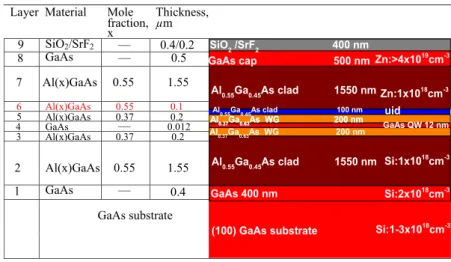
The LOC single quantum well HPLD structure was grown by metal-organic chemical vapor deposition on a 2-inch n-type doped with Si 1–3 × 1018cm−3 (100) GaAs substrate. A 12 nm undoped GaAs quantum well is embedded in 200 nm undoped Al0.37Ga0.63As waveguide layers. Between a
1.550μm p-Al0.55Ga0.45As upper cladding layer and upper
waveguide layer, a 100 nm undoped Al0.55Ga0.45As layer is
placed. A 1.55μm lower cladding layer (n-Al0.55Ga0.45As) is
placed between the GaAs substrate and a 400 nm GaAs buffer layer. The distance between surface and quantum well is 2.35μm including the 500 nm GaAs cap layer, as shown in table1. The dopant used for the p-type AlGaAs cladding layer is Zn (1 × 1018cm−3) and for the n-type AlGaAs cladding layer is Si (1 × 1018cm−3). For the n-type and the p-type GaAs buffer and cap layers, respectively, dopants are Si 2× 1018cm−3and Zn> 4 × 1019cm−3. In order to study the effects of different process parameters such as dielectric thickness, annealing time and temperature on intermixing, the 2-inch wafer was cut into small pieces, some used as as-grown and others as samples intermixed under different process conditions. They were then compared both optically and chemically using elemental analysis through XPS depth profiling.
2
Thin layers of SiO2 ranging in thickness from 200 to
400 nm were deposited on LOC HPLD structures by RF sputtering (Leybold L 560 system) under 4 × 10⁻⁶torr, 200 sccm Ar gasflowing corresponding to 10 mTorr growth pressure with RF power of 100 W to induce out-diffusion of Ga and Al atoms. Suppression of QWI was achieved by 100 nm thick SrF2layers deposited by thermal evaporation.
Rapid thermal processing (RTP) was used to carry out dif-fusion of defects at high temperatures (AG associates mini-pulse series). During RTP, samples were sandwiched between fresh GaAs wafers in order to prevent loss of As. In order to understand the QWI effect on the optical properties of LOC HPLDs, photoluminescence (PL) measurements were formed after every process. The PL measurements were per-formed at low temperature (6 K) using cryostat (Cryo industries). Ar+gas laser(at 514.5 nm line) was used as the excitation source and the luminescence from the samples were focused on to a 1 m Jobin Yvon double grating mono-chromator system (Horiba Spectralink U1000) coupled to a cooled charge-coupled device (CCD) detection system. In order to understand the diffusion of the Ga, Al, As, atoms, depth resolved XPS measurements were carried out on the as-grown and thermally processed samples using an XPS system (PHI 5000 VersaProbe) employing a monochromated Al K x-ray source equipped with an Ar-ion gun for in-depth profiling.
3. Results and discussion
Figure1shows the effects of varying the annealing duration, temperature and encapsulant thickness on the QWI through photoluminescence signature of the quantum wells. All of the PL measurements were performed at 6 K. Figure1(a)
illus-trates the annealing temperature dependence of the PL spectra of LOC HPLD structures due to QWI. Samples with 200 nm sputtered SiO2were annealed at 850, 900, 950°C for three
minutes each. The relatively small shift at low annealing
temperatures accelerates at higher temperatures leading to the highest blueshift of 34 nm (77 meV disordering) at an annealing temperature of 950°C. It was found that annealing the samples with 200 nm SiO2layers for 3 min even at 950°C
is not sufficient to obtain a considerable blueshift of the LOC laser diode structures. According to Kuzuhara et al[21], the
degree of intermixing strongly depends on the thickness of the SiO2 together with the annealing temperature, hence, it
was decided to increase the thickness of the SiO2 layer in
order to obtain a higher degree of blueshift. Figure 1(b)
illustrates the PL spectra dependence of QWI on SiO2
thickness on LOC HPLD structures annealed at 950°C for three minutes. We found that under the same annealing conditions, the thicker the SiO2layer, the larger the blueshift.
The maximum blue shift of 55 nm(130 meV) was obtained in samples with 400 nm thick SiO2 layers. It is known that
annealing for a longer duration with the same annealing temperature results in higher disordering of the effective band gap of the quantum well [28]. In order to understand the
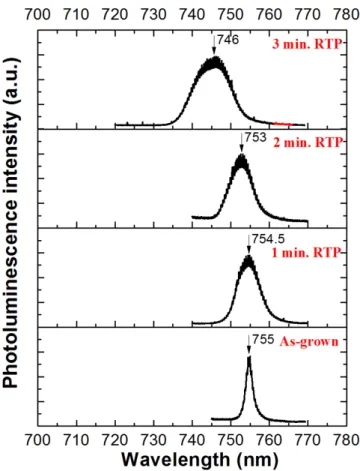
effects of the duration of annealing on QWI in HPLD struc-tures, 1, 2 and 3 min annealing at 950°C with 400 nm SiO2
overlayers was performed. Again, the maximum shift obtained after annealing for three minutes is 55 nm. Figure 1(c) illustrates the PL spectra of QWI for a 400 nm
SiO2sputtered sample annealed at 950°C. A small difference
in intermixing between 2 and 3 min annealing was observed (7 nm blue shift), thus it was considered unnecessary to anneal for longer durations. From these series of experiments, optimum annealing time, temperature and SiO2thickness for
QWI in LOC HPLD structures were determined as 3 min, 950°C and 400 nm thickness of SiO2, respectively.
Figure2illustrates the summary of the results of the PL data shown in figure 1 in terms of the shift of PL peak
wavelength and the width of the PL peaks (FWHM). In
figure 2(a) dependence of the PL shift on the annealing
temperature shows an exponential behavior. It is well known that the atomic diffusion coefficients are exponentially dependent on the temperature [29]. FWHM variation of the Table 1.Epitaxial structure of the high power laser diode used in this study. SiO2and SrF2are deposited on top of the 500 nm thick GaAs cap
layer. Epitaxial structure is shown on the right side of the plot. Abbreviations used in the epitaxial structure are clad; cladding, WG; waveguide.
peak also follows an exponential variation. The exponential behavior of the degree of intermixing and hence the amount of blueshift can be understood when the exponential dependence of the diffusion coefficient on temperature is considered. With a constant prefactor and activation energy, higher annealing temperatures lead to exponentially larger diffusion coefficients that translate into longer diffusion lengths and hence to larger PL peak wavelength shifts. The dependence of the PL shift on the SiO2 overlayer thickness
shows a linear dependence, seefigure2(b). The role of SiO2
in blueshifting of the bandgap luminescence is twofold. The first is related to the deposition conditions, hence sputtering generates point defects on the surface of the sample during the initial phase of deposition facilitating the diffusion of atomic species. The second function of the SiO2layer is to act as a
source of point defects and provide a sink for the out-dif-fusing atomic species with thicker SiO2 layers providing a
larger sink for out-diffusion. The width of the PL peak is a
Figure 1.Photoluminescence spectra of HPLD dependence on(a) annealing temperature, (b) encapsulant thickness, and (c) annealing time.
Figure 2.Left axis of thefigure shows the PL shift while the right side of the figure shows the FWHM variation of the peaks. The left and right axis is common for parts a,b and c, PL shift and FWHM of the PL emission, respectively. Thefilled symbols in each figure correspond to the PL shift while the blank symbols to the PL width(FWHM) variation of the peaks. (a) Annealing temperature, (b) encapsulant thickness,(c) annealing time dependence of the PL shift and the broadening of the quantum well luminescence.
4
measure of the spatial fluctuations of the quantum well potential. It increases with increasing spatial fluctuations. Contributions from locally varying quantum wells of different potential wells make up the PL peak. Close inspection shows that the width of the PL peak for the sample with 400 nm SiO2(figure 2(b)), has seemingly two distinct contributions.
In addition to the strong high energy peak, a low intensity wide tail suggests that the local variations of the potential are minimized. As the quantum well is quite narrow and is composed of a limited number of GaAs layers, dissolution of the layers creating point defects and interdiffusion of Al into GaAs can be considered to be discreet, hence it seems that the islands of newly created local potentials(due to diffusion of Al) enlarging at the expense of the previously pristine sections of the same layers to produce a sharp blue-shifted peak along with a tail, originate from leftover virgin portions of the layer on the quantum well. Finally,figure2(c) depicts
the linear dependence of PL peak wavelength shift on annealing duration dependence. The FWHM of the lumines-cence peaks also shows linear dependence on the duration of annealing. Considering that the PL emission wavelength is proportional to the square of the width of the quantum well and that the diffusion length is proportional to the square root of time, the linear dependence of the PL shift on the duration of annealing is expected[29]. The linewidth of a PL peak is a
function of crystalline disorder and therefore an increase in the width of the PL peaks with annealing time is also expected.
Suppression of QWI is as necessary as the enhancement of QWI because the band gap of the active waveguide region where the current is injected needs to be preserved during annealing for the QWI enhancement of the cavity edges in order to maintain the design wavelength. Thinfilms of ther-mally deposited SrF2 were successfully demonstrated to
inhibit QWI[30]. In this study, 100 nm of thermally deposited
SrF2 was used in order to suppress QWI in LOC HPLD
structures, which is illustrated in figure 3. A maximum blueshift of 9 nm was observed in samples with 100 nm SrF2
annealed for three minutes at 950°C. This is to be compared with the blueshift of 55 nm for the same duration of annealing and temperature. In this study, suppression of intermixing in a LOC laser diode structure, with a 2.35μm (cladding and waveguide) thick epitaxial overlayer between the quantum well and the surface, resulted in 9 nm disordering after 3 min of annealing at 950°C. This result is quite promising to prevent QWI in the active region of the HPLD structure.
Depth-resolved XPS analysis was used to understand the relationship between the luminescence peak wavelength shifts and diffusion of various elements in thermally processed samples using the IFVD mechanism, by comparing an as-grown sample and the sample that showed a 55 nm(130 meV) blue shift which was annealed with a 400 nm SiO2sputtered
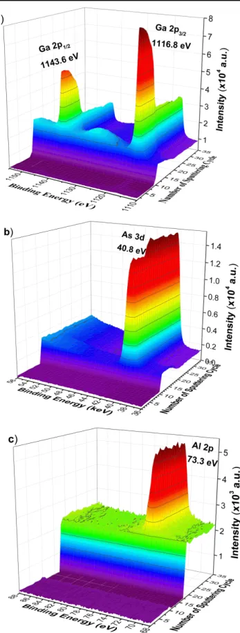
layer at 950°C for 3 min. Ga, As, Al, Si, O and C were followed through Ar+ depth profiling. XPS spectra were collected at each of the 35 sputtering intervals (cycles) to generate the depth profile. Figure4shows representative XPS plots for Ga(2p1/2) and Ga(2p3/2), Al(2p), and As(3d) lines of the elements for the processed sample. A detectable but small
amount of carbon contamination due to atmospheric exposure is observed on the surface of the samples. Carbon is observed in only thefirst sputter cycle with a binding energy of about 283.1 eV which corresponds to C–C binding (figure not shown).
The most significant element in the QWI of a GaAs/ AlGaAs crystal structures is Ga, it being the principal migrating element during annealing. In XPS, Ga is typically monitored using Ga(2p) either through Ga(2p1/2) or Ga(2p3/2) lines. In figure 4(a) we present the spectra for both Ga(2p)
peaks. Once most of the SiO2layer is sputtered away, at about
the 10th sputter cycle, Ga(2p) peaks appear with binding energies of 1116.8 eV and 1143.7 eV which are associated with Ga(2p3/2) and Ga(2p1/2) lines, respectively (see
figure4(a)). The integrated peak intensity of the Ga 2p 3/2
and the Ga 2p ½ becomes generally different and the ratio is Ga 2p 3/2 to Ga 2p ½ is generally given by 2 [31]. This is
related to occupancy of the levels split, 2p 3/2 and 2p 1/2 due to the spin–orbit coupling. The integrated intensity ratio of the obtained Ga 2p 3/2 and 1/2 is 2.002 which is theo-retically what it is expected. A As(3d) spectrum of the intermixed sample appears at the 10th sputter cycle where O(1s) and Si(2p) peaks start to disappear corresponding to the end of the SiO2layer (figure5). Details of the figure will be
given in the next paragraph. The XPS peak for arsenic is acquired for As(3d) photoelectrons and GaAs, As2O3, GaAs
native oxide, both triple and quintuple charged As, are the common chemical states for As(3d) lines. The As(3d) binding
Figure 3.The effects of SrF2layers on the photoluminescence
energies for these chemical states are 40.8 eV, 44.1 eV, 44.8 eV and 45.6 eV, respectively [32]. In our data the
binding energy of As(3d) is observed at 40.8 eV corresp-onding to GaAs as expected, see figure 4(b). Figure 4(c)
shows the Al(2p) spectrum of the intermixed sample starting at the 18th sputter cycle where the AlGaAs cladding layer is placed. Most common chemical states of Al(2p) are Al metal (72.6 eV), aluminosilicate (74.4 eV), Al-oxide (74.6 eV) and Al-foil (75.6 eV). It is clear that the peak in the figure observed at 73.3 eV corresponds to the metallic state of Al.
Depth distribution of the relevant atomic species for both as-grown as well as thermally processed samples are shown in figure 5. The data demonstrates diffusion of Ga atoms towards the surface which results in interdiffusion of Ga vacancies towards the quantum well region. After XPS ana-lysis, the depth profile of the sputtered crater was measured using a Dektak surface profilometer which is shown as an inset infigure5. According to this data, the depth profile can be divided into three regions; the first region is the 400 nm encapsulated SiO2 layer, the second region is the 500 nm
GaAs cap layer and the third is approximately 900 nm of the AlGaAs cladding layer. The demonstration of intermixing is described by comparing the as-grown sample with the inter-mixed sample. In the second region, where the GaAs cap layer is located, we observe that both Ga and As concentra-tions deviate from stoichiometry and are Ga-enriched in both the intermixed and as-grown samples. This is the well-known preferential sputtering effect [33], which explains the
observed Ga-enriched region. Fortunately, a comparison of the as-grown and intermixed samples is still possible. In the second and third regions, Ga concentration in the intermixed sample is higher than the as-grown sample which shows the migration of Ga atoms away from active region and the AlGaAs waveguide layer, towards the surface. The ratio of Ga(2p) concentration in the intermixed and as-grown samples is 1.24. A similar behavior holds also for the Al concentration profile. This is direct evidence of the diffusion of Al and Ga atoms due to thermal treatment. Diffusion of Al from the AlGaAs cladding layer into the GaAs cap layer is also clearly observed. The amount of Al in the second region reaches almost to 5% upon thermal treatment where it previously did not exist, even to the point of penetrating into the SiO2layer.
Finally, the amount of As decreases upon thermal treat-ment in both the second and third regions. In addition to the changes in the concentrations of Ga, we note that the Ga profile for the intermixed sample shifts towards the surface at the AlGaAs/GaAs interface, a clear indication of Ga migra-tion towards the surface. However, expected observamigra-tion of Ga atoms throughout the encapsulant layer (SiO2) has not
been realized. Instead, a small percentage of Ga atoms dif-fuses into the SiO2 and GaAs cap layer rapidly decaying
towards the surface, see figure 5. There might be several reasons for this. First, as reported in[25], the small amount of
Ga in the SiO2 layer can only be recognized with Auger
electron spectroscopy which we did not utilize. Second, in such LOC HPLD structures (table 1), for short periods of Figure 4.Spectral surfaces of depth-resolved XPS data,(a) Ga(2p1/2)
and Ga(2p3/2), (b) As(3d) and (c) Al(2p) lines of the quantum well
intermixed samples. The soft wide peak in(a) is the plasmon loss peak. Note that the peak positions do not change with depth, indicating no change in the chemical environment of the species throughout the sample.
6
annealing and annealing temperatures performed in this study, Ga atoms may not have had time to penetrate throughout all of the SiO2layer. XPS results obtained in the present study
shows that Ga and Al diffusion throughout the thermally processed LOC samples correlates well with the observed PL peak shifts indicating successful QWI in LOC HPLD struc-tures at relatively low temperastruc-tures and durations.
4. Conclusions
HPLDs are performance limited during lasing due mainly to COMD. Use of quantum well intermixing to create NAM regions at the cavity edges and using LOC are the main solutions in order to minimize COMD. The optimum condi-tions for the IFVD technique for both enhancement and suppression of QWI in actual LOC laser diode structures in an AlGaAs/GaAs structure have been determined and correlated with Ga and Al diffusion using both low temperature PL spectroscopy and XPS depth profiling for the first time. AlGaAs/GaAs LOC HPLD structures were used where the quantum well was buried 2.35μm below the surface (without the encapsulating layer), typical for LOC cavities. A 55 nm (130 meV) blueshift in the PL peak due to QWI and only 9 nm (19.8 meV) blueshift during suppression of QWI, respectively, were obtained at 950°C for 3 min in a RTP. XPS analysis shows migration of Ga and Al atoms towards the surface correlating with the observed blueshift.
Acknowledgments
The authors would like to thank Professor Dr Raşit Turan and İlker Yıldız of METU Central laboratory for XPS data acquisition. Thefinancial support of Ermaksan A S is grate-fully acknowledged.
References
[1] Henry C H, Petroff P M, Logan R A and Merritt F R 1979 J. Appl. Phys.50 3721–32
[2] Marsh J H 2007 Laser Technik J.4 32–5
[3] Hempel M, Tomm J W, Ziegler M, Elsaesser T, Michel N and Krakowski M 2010 Appl. Phys. Lett.97 231101
[4] Diechl R 2000 High-Power Diode Lasers: Fundamentals, Technology, Applications(Germany: Springer)
[5] Alferness R C, Koren U, Buhl L L, Miller B I, Young M G, Koch T L, Raybon G and Burrus C A 1992 Appl. Phys. Lett. 60 3209–11
[6] Morita T, Nagakura T, Torii K, Takauji M, Maeda J, Miyamoto M, Miyajima H and Yoshida H 2013 IEEE J. Sel. Top. Quantum Electron.19 1502104
[7] Marsh J H 1993 Semicond. Sci. Technol.8 1136–55 [8] Epperlein P W 2013 Semiconductor Laser Engineering,
Reliability and Diagnostics: A Practical Approach to High Power and Single Mode Devices(UK: Wiley)
[9] Wen X, Chi J Y, Koteles E S, Elman B and Melman P 1990 J. Electron. Mater.19 539–42
[10] Yu J S and Chung K S 2007 Semicond. Sci. Technol.22 919–24
[11] Du S C, Fu L, Tan H H and Jagadish C 2010 Semicond. Sci. Technol.25 055014
Figure 5.XPS depth profile of an intermixed and as-grown sample. The inset in the right side top of the plot shows the epitaxial layers up to the GaAs QW of the grown high power laser diode structure. It shows the depth performed in the XPS measurement. The inset at the right side bottom is the three-dimensional depth profile of the sputtered crater after the XPS measurements have been done. The obtained depth is 1.81μm for the as-grown and 1.83 μm (not shown) for the intermixed sample. The abbreviations used in the figure ‘I’ mean intermixed, ‘A’ as-grown.
[12] Helmy A S, Murad S K, Bryce A C, Aitchison J S, Marsh J H, Hicks S E and Wilkinson C D W 1999 Appl. Phys. Lett.74 732–4
[13] Deenapanray P N K, Tan H H, Cohen M I, Gaff K, Petravic M and Jagadish C 2000 J. Electrochem. Soc.147 1950–6
[14] Deenapanray P N K and Jagadish C 2001 J. Vac. Sci. Technol. B19 1962–6
[15] Rao E V K, Hamoudi A, Krauz P, Juhel M and Thibierge H 1995 Appl. Phys. Lett.66 472–4
[16] Pepin A, Vieu C, Schneider M, Launois H and Nissim Y 1997 J. Vac. Sci. Technol. B15 142–53
[17] Doshi S, Deenapanray P N K, Tan H H and Jagadish C 2003 J. Vac. Sci. Technol. B21 198–203
[18] Kowalski O P, Hamilton C J, McDougall S D, Marsh J H, Bryce A C, De La Rue R M, Vgele B, Stanley C R, Button C C and Roberts J S 1998 Appl. Phys. Lett.72 581–3
[19] Allen E L, Pass C J, Deal M D, Plummer J D and Chia V F K 1991 Appl. Phys. Lett.59 3252–4
[20] Gonjito I, Krauss T, Marsh J H and De La Rue R M 1994 IEEE J. Quantum Electron.30 1189–95
[21] Kuzuhara M, Nozaki T and Kamejima T 1989 J. Appl. Phys. 66 5833–6
[22] Matsushita S, Terada S, Fujii E and Harada Y 1993 Appl. Phys. Lett.63 225–7
[23] Gyulai J, Mayer J, Mitchell I V and Rodriguez V 1970 Appl. Phys. Lett.17 332–4
[24] Haga T, Tachino N, Abe Y, Kasahara J, Okubora A and Hasegawa H 1989 J. Appl. Phys.66 5809–15
[25] Konig U and Sasse E 1983 J. Electrochem. Soc.130 950–2 [26] Fu L et al 2002 J. Appl. Phys.92 3579–83
[27] Hofstetter D, Maisenholder B and Zappe H P 1998 IEEE J. Sel. Top. Quantum Electron.4 794–802
[28] Ooi B S, McIlvaney K, Street M W, Helmy A S, Ayling S G, Bryce A C and Marsh J H 1997 IEEE J. Quantum Electron. 33 1784–92
[29] Lie J T 2000 Semiconductor Quantum Well Intermixing: Material Properties and Optoelectronic Applications (Singapore: Gordon and Breach Science) ch 2
[30] Beauvais J, Marsh J H, Kean A H, Bryce A C and Button C 1992 Electron. Lett.28 1670–2
[31] Colón Santana J A 2015 Quantitative Core Level Photoelectron Spectroscopy(CA, USA: Morgan & Claypool)
[32] Crist B V 2000 Handbooks of Monochromatic XPS Spectra (UK: Wiley)
[33] Singer I L, Murday J S and Comas J 1981 J. Vac. Sci. Technol. 18 161–3
8