Semiconductor Nanoplatelet Heterostructures Enhanced
via Combinations of Colloidal Atomic Layer Deposition
and Hot Injection Shell Growths
A THESIS SUBMITTED TO
THE GRADUATE SCHOOL OF ENGINEERING AND SCIENCE
OF BILKENT UNIVERSITY
IN PARTIAL FULFILLMENT OF THE REQUIREMENTS FOR
THE DEGREE OF
MASTER OF SCIENCE
IN
MATERIALS SCIENCE AND NANOTECHNOLOGY
By
Ulviyya Quliyeva
July 2019
i
SEMICONDUCTOR NANOPLATELET HETEROSTRUCTURES ENHANCED VIA COMBINATIONS OF COLLOIDAL ATOMIC LAYER DEPOSITION AND HOT INJECTION SHELL GROWTHS
By Ulviyya Quliyeva July 2019
We certify that we have read this thesis and that in our opinion it is fully adequate, in scope and in quality, as a thesis for the degree of Master of Science.
___________________________________________ Hilmi Volkan Demir (Advisor)
___________________________________________ Dönüş Tuncel
___________________________________________ Evren Mutlugün
Approved for the Graduate School of Engineering and Science:
___________________________________________ Ezhan Karaşan
ii
ABSTRACT
SEMICONDUCTOR NANOPLATELET HETEROSTRUCTURES
ENHANCED VIA COMBINATIONS OF COLLOIDAL ATOMIC
LAYER DEPOSITION AND HOT INJECTION SHELL GROWTHS
Ulviyya Quliyeva
M.S. in Materials Science and Nanotechnology Advisor: Hilmi Volkan Demir
July 2019
One of the most promising families of semiconductor nanocrystals in colloidal optoelectronics and nanophotonics is considered to be colloidal quantum wells, also commonly referred to as nanoplatelets (NPLs). Possessing an atomically flat structure, NPLs feature unique properties including spectrally-resolved and tunable light-hole- and heavy-hole transitions accompanied by their respective giant oscillator strengths. CdSe, CdS and CdTe, making the first colloidal NPLs synthesized in core-only structure, portray distinct qualities necessary for light-harvesting and -generating applications. However, going beyond the core structure, there are many properties that are highly enhanced by growing crown and/or shell layers around core NPLs. While the crown growth takes place anisotropically in lateral directions, the shell layer covers the entire NPL surface, combinations of which enable NPL heterostructures in new architectures. Depending on the electronic alignment of parts of the NPL heterostructure and the resulting confinement of electron-hole wave functions, these hetero-NPLs can be type-I or type-II. In type-I electron-hole pairs are confined in the core-NPL and recombination occurs in a direct pathway. In type-II electron-hole wave function is separated into different semiconductor layers, resulting in spatially indirect recombination. In this thesis, we synthesized and showed thin- and thick-shell grown heterostructures of type-I CdSe/ZnS NPLs using hot-injection (HI) for the first time particularly for these semiconductor NPLs. Unlike the typical colloidal atomic layer deposition (c-ALD) technique, which produces NPL heterostructures with low quantum yield (QY) and low chemical and optical stability, our approach yields CdSe/ZnS NPLs of almost unity (100%) quantum yield (QY) and improved chemical stability, tested by washing the same samples rigorously up to 6 times with ethanol with little change observed in the QY. Additionally, unparalleled thermal and optical aging endurances is achieved in aging tests. These tests experimentally demonstrated
iii
that, elevated to 400 K, HI thick-shelled NPLs can retain up to 65% of their emission intensity in the colloidal form and 52% of that in the film. This level of high stability creates a great opportunity for employing these NPLs for high-temperature applications. Also, in the thesis, we synthesized and studied CdS/CdSe core/crown, CdS/CdZnS core/c-ALD grown and CdS/CdSe/CdZnS core/crown/c-ALD shell-grown heterostructures of NPLs. Here the starting-template CdS NPLs are considered to be unique in terms of their emission in the blue region, which may open up new opportunities for NPL lasing in this spectral region. Nominally CdS NPLs are folded due to great lateral sizes. However, in this research work, when coated with crown and shell layer, these particles unfold. The unrolled CdS/CdSe core/crown NPLs are found to exhibit relatively higher QY up to 15-20% in its class of CdS core-seeded NPLs. The findings of this thesis reveal that such heterostructures of the NPLs are very rich in terms of variety of the quantum architectures one can achieve using them as working model systems.
Keywords: Colloidal quantum wells, nanoplatelets, core/crown, core/shell,
iv
ÖZET
KOLOİDAL ATOMİK KATMAN KAPLAMA VE SICAK
ENJEKSİYON KABUK KAPLAMA YÖNTEMLERİNİN
BİRLEŞİMİYLE GELİŞTİRİLEN YARI İLETKEN NANOLEVHA
HETEROYAPILARI
Ulviyya QuliyevaMalzeme Bilimi ve Nanoteknoloji, Yüksek Lisans Tez Danışmanı: Hilmi Volkan Demir
Temmuz 2019
Nanolevhalar olarak da bilinen kolloidal kuantum kuyuları, kolloidal optoelektronik ve nanofotonik alanlarındaki önemli yarı iletken nanokristal malzeme gruplarından biridir. Atomik boyutları ve levhayı andıran düz yapıları sayesinde bu malzemelerin optik özellikleri istenildiği şekilde değiştirilebilir ve yine aynı sebepten ötürü bu malzemeler dev osilatör gücü gibi benzersiz özelliklere sahiptirler. CdS, CdSe ve CdTe, çekirdek şeklinde sentezlenmiş ilk yarıiletken nanolevhalar, ışık hasatı ve üretimi uygulamaları için gerekli özellikleri sergilerler. Ancak, bu optik ve kimyasal özellikler, çekirdeğin etrafında taç ve kabuk tabakaları büyütülerek iyileştirilebilir. Taç katmanı büyümesi yanal yönlerde gerçekleşirken, kabuk katmanı nanolevha yüzeyinin tamamını kaplar. Bu iki farklı katman büyütme tekniği birlikte kullanılarak yeni nanolevha heteroyapıları oluşturulabilir. Elektron ve deşik dalga fonksiyonlarının elektronik lokalizasyonuna bağlı olarak, bu hetero-nanolehvalari Tip-I ve Tip-II olarak ayrılır. Eksiton çiftlerinin sadece bir bölgeye hapsolduğu durumda Tip-I yapı oluşur ve rekombinasyon doğrudan gerçekleşir. Elektron ve deşik farklı yarıiletken katmanlarında lokalize olduğunda Tip-II yapı oluşur ve dolaylı rekombinasyon gerçekleşir. Bu tez çalışmasında, Tip-I yapıya sahip CdSe/ZnS ince ve kalın-kabuk nanolehva heteroyapıları ilk defa sıcak enjeksiyon yöntemi kullanılarak yapılmıştır. Düşük kuantum verime ve düşük kimyasal ve optik kararlılığa sahip heteroyapılarla sonuçlanan kolloidal atomik katman kaplama tekniğinin aksine, sıcak enjeksiyon yöntemi ile neredeyse %100 kuantum verime sahip ve en fazla 6 defa etanolle yıkadıktan sonra bile kuantum verimi neredeyse değişmeyen nanolehvalar üretilmiştir. Öte yandan sıcak enjeksiyon yöntemi ile sentezlenen kalın-kabuk nanolevhaların, 400 K sıcaklığında kolloidal şeklinde fotolüminesans verimliliğinin %65’ini ve film şeklinde fotolüminesans verimliliğinin %52’sini koruduğunu gösteren yaşlanma
v
testleriyle benzersiz termal ve optik yaşlanma dayanıklılığı tespit edilmiştir. Bu yüksek seviyedeki dayanıklılık, bahsi geçen nanolevhaları yüksek sıcaklık uygulamaları için kullanılmasına fırsat yaratır. Tez çalışmasının bir başka kısmı, CdS nanolevhalarının ve onların CdS / CdSe çekirdek / taç, CdS / CdZnS çekirdek / c-ALD kabuk ve CdS / CdSe / CdZnS çekirdek / taç / c-ALD kabuk heteroyapılarının sentezini de kapsamaktadır. Nanolevhalar arasında CdS yalnız mavi bölgede ışıma yapmaktadır, bu özellik lazer teknolojisinde yeni kapılar açabilir. Normalde, büyük yanal boyutları nedeniyle CdS yapısal anlamda katlanmaktadır. Bu araştırma çalışmasında, taç ve kabuk tabakası ile kaplandığında, bahsedilen nanolevha katlanmasının önüne geçilmektedir. Bu CdS / CdSe çekirdek / taç nanolevhalarında, yalnızca çekirdek yapıdaki CdS nanolevhalarıyla karşılatırıldığında, kuantum verimi %15-20’ye kadar artış göstermektedir. Nihai bulgular, bu nanolevha heteroyapılarının çeşitli kuantum mimarileri yönünden oldukça zengin olduğunu göstermektedir.
Anahtar sözcükler:Koloidal kuantum kuyuları, nanolevhalar, çekirdek/taç, çekirdek/kabuk, sıcak enjeksiyon, koloidal atomik katman kaplama.
vi
Acknowledgement
When I started my MSc degree at UNAM, I did not know what to expect and was overwhelmed with the amount of new information I would need to absorb. However, thanks to all people who supported me both academically and morally I took many steps and came closer to becoming a true researcher.
First of all, I would like to deeply thank Prof. Hilmi Volkan Demir, my supervisor, for his constant support and guidance during the whole time at Bilkent University and UNAM. He helped me to understand what it is like to be a true researcher in his own example. He taught me that it takes hard work, vision, perseverance, good communication, and patience to create a suitable environment for high-quality research and to realize your goals. I would like to, especially, thank him for great patience he showed towards my mistakes and his advices in order to avoid them in the future.
Also, I would like to express my great gratitude to Assoc. Prof. Dönüş Tuncel and Assoc. Prof. Evren Mutlugun for finding time in their busy schedules and becoming jury members of my thesis.
Next, I want to thank the past and current members of Demir Research Group. I would like to thank Dr. Yemliha Altintas for working together on CdSe/ZnS core/hot-injection shell synthesis. I acquired a lot of precious theoretical and practical knowledge by being part of this project. I want to express my gratitude to Özgün Akyüz and Emre Ünal for their constant support and assistance in and out of the laboratory, especially for patiently answering every question I had for them. I want to thank Didem Dede for introducing me to the colloidal nanoplatelet synthesis and guiding me on the way. I would like to thank Onur Erdem from our team for always, and without hesitation, sharing his invaluable experience, guiding me in my work and being a true example and a true friend. Also, Ayşe Bilgehan Başpınar, Dr. Nina Sheremet and Ekin Bircan Boşdurmaz for always being there for me when I needed the most. I would like to thank Farzan Shabani and Furkan Işık for their great sense of humour and making laboratory work highly enjoyable. I want to thank İbrahim Tanrıöver, Mustafa Sak, Selim İrfan Bozdoğan, and Nima Taghipour for making late office and laboratory hours full of good moments and sharing their knowledge. I would like also to thank Birsen Bilgili for her kindness and always caring about our group. I
vii
want to thank Dr. Kıvanç Güngör, Dr. Volodymyr Sheremet, Dr. Savaş Delikanlı, Dr. Murat Olutaş, Dr. Neghar Gheshlaghi, Dr. Yusuf Keleştemur, Hamza Humayun, Sina Foroutan, Joudi Maskoun, Ramazan Özbekand Hüseyin Bilge Yağcı from our group. My time at Bilkent University UNAM gave me a lot of priceless friendships. I want to specially thank my friends Assel Amirzhanova, Eliza Sopubekova, Koray Yavuz, Mehdi Ramezani, Mohammad Fathi Tovini, and Ecem Yelekli for their great friendship and experiences we shared. I want to also thank my friends from UNAM: Roujin Ghaffari, Yasaman Sheidaei, Mohammad Morsali, Engin Can Sürmeli and Onur Çakıroğlu.
I want to thank all of UNAM faculty members, the technical and administrative staff. I would like to especially thank Mustafa Güler, Övünç Karakurt, Dr. Gökçe Çelik, Ayşegül Torun, Duygu Kazancı, Mustafa Doğan and Songül Zeybek.
Finally, I want to deeply thank my family for always encouraging and supporting me from the distance.
viii
Contents
Chapter 1 Introduction ... 1
Chapter 2 Synthesis methods of colloidal nanoplatelets ... 4
2.1 Core synthesis ... 4
2.2 Crown growth ... 8
2.3 c-ALD shell growth ... 9
2.4. Hot – injection shell growth ... 11
Chapter 3 Characterization methods of colloidal nanoplatelets ... 13
3.1. Optical characterization ... 13
3.1.1. UV-vis spectroscopy ... 14
3.1.2. Fluorescence spectroscopy ... 16
3.1.3. Quantum yield measurement ... 17
3.2. Structural characterization ... 18
3.2.1. Transmission Electron Microscopy (TEM) ... 18
3.2.2. X-ray powder diffraction spectroscopy ... 21
3.2.3. X-ray photoelectron spectroscopy ... 23
3.3. Aging tests ... 24
4.1. Chemicals ... 25
4.2. CdSe core synthesis ... 25
4.3. CdSe/ZnS core/colloidal atomic layer deposition shell synthesis ... 28
4.4. CdSe/ZnS core/hot-injection shell synthesis ... 30
4.5. CdS core synthesis ... 33
4.6. CdS/CdSe core/crown synthesis ... 34
4.7. CdS/CdSe/ZnS core/crown/ colloidal atomic layer deposition shell synthesis36 5. Characterization of nanoplatelet heterostructures coated with crown and shell layers ... 39 5.1. Optical characterizations ... 39 5.1.1. CdSe/ZnS hot-injection NPLs ... 39 5.1.2. CdS NPL heterostructures ... 47 5.2. Structural characterizations ... 50 5.2.1. CdSe NPL heterostructures ... 50 5.2.2. CdS NPL heterostructures ... 55
ix
5.3. Aging tests ... 56
5.3.1. Thermal aging ... 56
5.3.2. Optical aging (UV test) ... 60
Chapter 6 Conclusion ... 62
Bibliography ... 64
x
List of Figures
1.1 Various NPLs synthesized at our laboratory emitting at different wavelengths of the color spectrum.
2.1 Possible pathways for CdSe core NPLs growth mechanism. After the initial seed growth there are potentials routes: (1) Lateral extension happens when the seeds self-organize on the seed level or in patches (3), the seeds extend in lateral direction through the continuous reaction of precursors (2).
2.2 The Schlenk line apparatus and utilities employed for the synthesis under non-ambient conditions at our laboratory.
2.3 Schematic depiction of processes going on upon excitation of (a) type – I CdSe/CdS core/crown heterostructures and (b) type – II CdSe/CdTe.
2.4 A photo image of our CdSe/CdS core/ c-ALD shell heteronanoplatelet samples coated with 1, 2, 3, 4, 5- and 6-ML c-ALD shells at our laboratory: from left to right. 3.1 General scheme for a typical double-beam UV-Vis spectrometer.
3.2 Example of absorption spectrum of 4 ML CdSe NPL synthesized at our laboratory showing heavy-hole and light-hole electron transitions.
3.3 Example of PL emission spectrum of 4 ML CdSe NPL sample synthesized at our laboratory.
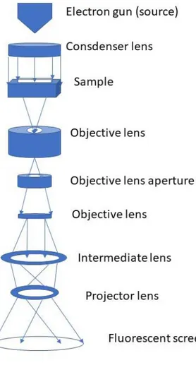
3.4 A typical TEM.
3.5 Schematic representation of TEM column.
3.6 Examples of HAADF-STEM images of (a) CdSe NPLs and (b) CdS NPLs synthesized at our laboratory.
3.7 A schematic of Bragg’s law working principle. 3.8 a) XRD spectra of CdSe NPLs, b) XRD instrument.
4.1 HAADF-STEM images of 4 ML NPLs synthesized using a) Cd acetate anhydrate, b) Cd acetate monohydrate, c) Cd acetate dihydrate.
4.2 HAADF-STEM images showing influence of the Cd acetate amount on the final shapes of CdSe NPLs while all other conditions are kept the same: (a) 90 mg, (b) 100 mg, (c) 110 mg, and (d) 120 mg.
xi
4.3 Photographs of a) CdS/CdSe inverted type-I NPLs and b) CdS/CdSe/S
2-core/crown/ c- ALD semi-layer NPLs when illuminated with a UV light source in the dark.
5.1 Absorption and PL emission spectra of CdSe/ZnS hot-injection a) thin-shell and b) thick-shell samples.
5.2 a) Absorption and PL emission of the aliquots of the thin-shell sample taken in certain time intervals and b) those of the final cleaned sample. a) Reprinted with permission from [2].
5.3 a) PL emission and b) absorbance spectra and images of CdSe/ZnS hot-injection core/shell samples based on the variation of OA amount in the synthesis. Reprinted with permission from [2].
5.4 a) PL emission and b) absorbance spectra and c) images of CdSe/ZnS hot-injection core/shell samples based on the variation of OLA amount in the synthesis. Reprinted with permission from [2].
5.5 (a) Absorbance and (b) PL spectra of CdSe/ZnS core/c-ALD shell heterostructures synthesized at our laboratory.
5.6 (a) Absorption and (b) PL emission spectra examples of two CdS NPL samples synthesized at our laboratory.
5.7 Absorption and PL emission spectra of CdS/CdSe NPLs for the cases (a) when 1 mL Cd crown and 1 mL of TOP-S precursor, (b) when 500 µL Cd crown and 0.5 mL TOP-S precursor, and (c) were used.
5.8 Absorption and PL emission spectra of CdS/c-ALD ZnS/hot-injection ZnS shell NPLs.
5.9 a) HAADF-STEM images of CdSe NPLs with irregular (left) and square (right) shapes; HR-TEM images of CdSe/ZnS core/hot-injection thin-shell NPLs
synthesized using b) irregular shaped CdSe core NPLs and c) square shaped CdSe NPLs; and d) HR-TEM images of thick-shell CdSe/ZnS NPLs.
5.10 HAADF-STEM images of CdSe/ZnS core/hot-injection thin-shell NPLs where it is evident that their tip parts are detached during synthesis, cooling or cleaning. 5.11 HR-TEM images of free-standing CdSe/ZnS core/hot-injection thick-shell (left) and thin-shell (right) NPLs.
5.12 SEM images of CdSe NPLs.
5.13 XRD data of our CdSe core, CdSe/ZnS core/c-ALD shell and CdSe/ZnS core/hot-injection shell NPLs. Reprinted with permission from [2].
xii
5.14 TEM images of CdS NPLs synthesized at our laboratory: the left image shows the typical rolled CdS NPL structures and the right one depicts their actual shape when unrolled.
5.15 SEM images of CdS/CdSe/CdZnS core/crown/c-ALD shell NPLs synthesized at our laboratory.
5.16 a) Normalized PL intensity values of colloidal CdSe/ZnS core/HI shell NPLs, both for the thin-shell and thick-shell samples, during temperature elevation from room temperature to 525 K under inert Ar gas and b) integrated PL intensity of the thin-shell and thick-shell CdSe/ZnS HI NPLs. Reprinted with permission from [2]. 5.17 Images from our setup constructed to implement thermal tests in solution under inert gas.
5.18 a) Normalized PL intensity values and b) the change of both normalized and integrated PL spectra, wavelength (nm) and FWHM values of deposited CdSe NPL, CdSe/ZnS HI thin-shell, CdSe/ZnS HI thick-shell, CdSe/ZnS c-ALD thin-shell and CdSe/ZnS c-ALD thick-shell samples while heating the quartz films from 300 to 525 K under ambient conditions, c) heating and cooling cycling of the same samples in the following temperature ranges: from 300 to 350 K; from 300 to 400 K; from 300 to 450 K and from 300 to 500 K. Reprinted with permission from [15].
5.19 UV lamp illumination test results of CdSe/ZnS core/ shell NPL samples that were synthesized with our HI-shell method. Reprinted with permission from [2].
xiii
List of Tables
5.1 QY (%), FWHM and emission peak (nm) values of 10 distinct Thin-Shell and Thick-Shell samples.
5.2 QY (%), PL emission wavelength (nm) and FWHM (nm) values based on the OA amount used (500 µL OLA is used in each case).
5.3 QY (%), PL emission wavelength (nm) and FWHM (nm) values based on the OLA amount used (500 µL OA is used in each case)
1
Chapter 1
Introduction
Starting from the 80s of the last century, semiconductor nanocrystals (NCs) have become one of the most extensively studied areas of the nanoparticle realm. One of the major breakthroughs came with the discovery of quantum size effect in NCs [3]. Semiconductor NCs, specifically, colloidal quantum dots (QDs) whose radii are smaller than or comparable to the bulk exciton Bohr radius, constitute a class of materials intermediate between molecular and bulk forms of matter. A straightforward and easy colloidal pathway to obtain monodisperse NCs was introduced by Bawendi [4]. The advancement in the synthesis of various shapes of semiconductor nanoparticles continued with nanorods, nanowires, nanotetrapods and finally leading to nanoplatelets (NPLs).
Nanoplatelets (NPLs), the so-called colloidal quantum wells, are free-standing quasi-two-dimensional nanosheets having strong one-dimensional quantum confinement. They feature a giant oscillator strength transition. They are fast colloidal fluorescent emitters exhibiting nanosecond lifetime at temperatures approaching cryogenic [5][6]. One of the advantages of NPLs over QDs is their large volume relative to QDs. Thus, NPLs show weaker Coulomb blockade effects and hence, permits enhanced charge injections without affecting quantum confinement. While synthesizing QDs requires precise control over 3 directions, in the case of NPLs only vertical thickness should be precisely controlled and manipulated. As a result of uniform vertical thickness, NPLs have narrow photoluminescence (PL), which is highly favorable for applications such as LEDs that need high color purity.
2
Nowadays, the main synthesis pathways for 2D materials include molecular beam epitaxy, exfoliation, and colloidal synthesis in solution [7][8]. Unlike the 2D systems which are produced through gas phase deposition, the number of atomic layers of nanoplatelets can be tuned down to single atomic layers, which is why they are often referred to as atomically flat [5].
In recent years, new NPL heterostructures (core/crown and core/shell) have been made to enhance chemical and optical properties of the core NPL structures such as photostability and PL QY. In most cases, especially those involving high temperature growth, shell layer leads to a strong enhancement of the PL QY [9]. On the other hand, in the core/crown structure outer crown layer acts as a exciton funnel that gathers excitons and channels them to the core [10] , which can be explained by the difference in dielectric constant of the core and crown materials.
In this thesis work, colloidal CdSe and CdS NPLs were synthesized and covered by using combinations of hot-injection (HI) grown ZnS shell layers and CdSe crown, colloidal atomic layer deposition (c-ALD) grown CdZnS layers. The main motivation of the synthesis of CdSe/ZnS core/HI shell is to produce environmentally and thermally stable shell structures. The HI shell deposition was mostly implemented by using CdS as an outer shell layer. However, because of the substantial distinction in CdSe and ZnS band gaps, this shell can produce better passivation. Therefore, enhanced NPLs can be synthesized for applications requiring elevated temperatures. When it comes to CdS, the motivation stems from the fact there is not much application of NPLs emitting at blue region of the colour spectrum. New core/crown recipe might improve QY and c-ALD shell growth and assist in uniform passivation of the rolled CdS NPLs and thus, opening up for the further improvement.
3
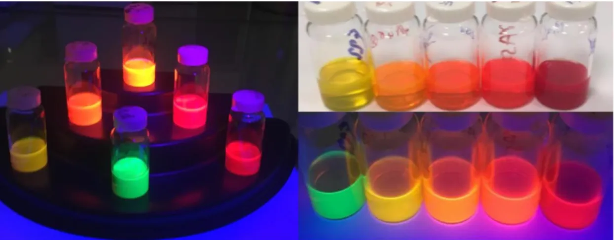
Figure 1.1: Various NPLs synthesized at our laboratory emitting at different wavelengths of the color spectrum.
4
Chapter 2
Synthesis methods of colloidal
nanoplatelets
2.1 Core synthesis
Efficient synthesis of colloidal core NPLs is a critical step for heterostructures to be grown on them. In recent years, among most extensively studied NPLs, CdSe, CdTe and CdS cores have been important in terms of their potential applications. They have tunable and narrow bandgap emission thanks to their monodispersity.To obtain pure 2D NPL cores with enhanced optical features and chemical stability, a good control of the reaction parameters (e.g., capping agents, molar ratio, temperature, time), along with the right choice of appropriate precursors (e.g., transition metals and chalcogens), is crucial. As a result, the intrinsically desired anisotropic growth can be preserved. Usually, −chloride, −carbonyl and −carboxylate precursors are employed as high-yielding metal precursors [5], [8], [11], [12]. The most distinguished and thoroughly explored core NPLs are CdSe nanoplatelets. Their thickness ranges from 2 to 8 monolayers (MLs) [13]. Among them 4 ML CdSe synthesis is the simplest, the least time-consuming, and requires the least material input. The as-synthesized NPLs are atomically flat, they have precise vertical thickness, and require minor cleaning by size-selective precipitation through the usage of polar solvents such as ethanol and methanol [5], [11], [12].
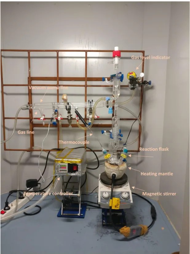
The synthesis of NPLs, in general, is carried out in an apparatus called Schlenk line consisting of two manifolds with numerous ports (Figure 2.2). One manifold is usually connected to vacuum pump and the other one to neutral gas (typically nitrogen or Argon). 4 ML CdSe core NPL synthesis usually involves Cd salt with a long hydrophobic chain, a non-coordinating solvent and a Se source in the form of elemental Se. The major CdSe synthesis pathway starts with preparing Cd(myristate)2
5
in methanol at room temperature and then filtering the residual Cd salt after the synthesis. The next stage involves a quite well-defined sequence of steps with minor variations:
• Adding 340 mg Cd(myristate)2, 24 mg Se and 30 mL octadecene (ODE) to a
100 mL flask,
• Degassing for some time,
• Adding Cd precursor with a relatively shorter chain at an elevated temperature at which the solution acquires a golden color, indicating the nucleation of particles having 4 ML thickness (usually around 195 oC),
• Starting a timer around 220 oC when Cd(myristate)
2 starts to decompose and
the actual growth starts,
• Continuing the reaction depending on the targeted lateral size (i.e., keeping longer for large area NPLs), and
• Finally, quenching the reaction with oleic acid (OA).
The synthesis of CdS NPLs was first discovered by Dubertret’s group [5]. In their case, unlike CdSe NPLs, CdS NPLs did not have sharp features and thus, had different subpopulations. They used Cd myristate as the Cd precursor and Zn acetate as the capping agent. Later, Peng et al. suggested different synthesis routes using Cd acetate dihydrate and, instead of degassing, they applied Argon bubbling [14]. Also, they used oleic acid as the ligand but also worked with other ligands such as myristic acid, stearic acid and melissic acid.
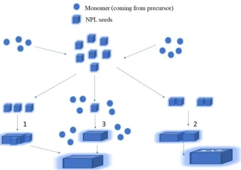
The major reaction stages in the NPL synthesis can be divided into the conversion of precursors to seeds, the nucleation and the growth. Through investigations using optical methods and transmission electron microscopy (TEM) it is suggested that the initial seed formation dictates thickness of NPLs with lateral extensions later in the subsequent growth stage. There are few hypothesized growth mechanisms for NPL core formation as reported by Dubertret et al. According to one potential mechanism, the lateral extension happens when the seeds self-organize on the seed level or in patches. In another proposed mechanism, the seeds extend in lateral direction through the continuous reaction of precursors (Figure 2.1) [15].
6
Figure 2.1: Possible pathways for CdSe core NPLs growth mechanism. After the initial seed growth there are potentials routes: (1) Lateral extension happens when the seeds self-organize on the seed level or in patches (3), the seeds extend in lateral direction through the continuous reaction of precursors (2).
7
Figure 2.2: The Schlenk line apparatus and utilities employed for the synthesis under non-ambient conditions at our laboratory.
Gas line
Vacuum pump line
Thermocouple
Heating mantle
Magnetic stirrer Temperature controller
Reaction flask Gas level indicator
8
2.2 Crown growth
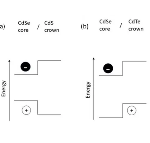
To improve optical properties of NPLs, anisotropic core/crown NPL heterostructures can be synthesized. The crown layer is an extension in the lateral direction and is atomically flat with the same thickness as the original core NPL. It is usually grown by choosing shorter-chain carboxylic acids, using different temperatures (usually lower) and making precursors more concentrated compared to those of the core. Depending on the size of the core, the resulting core/crown heterostructures can display properties related to either the core semiconductor or the crown semiconductor. According to the band structure of the formed heteronanoplatelets, the core/crown NPLs are divided into 2 types: type-I and type-II (Figure 2.3). In the type-I NPLs, the core is covered with a wider band gap material and both charge carriers (hole and electron) are confined inside the core NPL [10], [16]. The crown coating acts as an optical antenna for excitation funnelling the photogenerated NPLs and increasing the NPL’s emission. CdSe/CdS NPLs are a common example of type-I heteronanoplatelets. In the type-II nanoplatelets, electron and hole are confined in different parts of the heteronanoplatelets. As a result, charge carriers are separated between the core and crown regions [16], [17]. CdSe/CdTe heteronanoplatelets are a good example of type-II core/crown NPLs [17].
9
Figure 2.3: Schematic depiction of processes going on upon excitation of (a) type – I CdSe/CdS and (b) type – II CdSe/CdTe core/crown heterostructures.
The main synthesis process starts with the core synthesis as explained in Section 2.1 and its purification is carried out carefully beforehand. Then, in the case of CdS coating, a Cd crown precursor is synthesized separately. Usually, a mixture of Cd(acetate)2 dihydrate, OA and ODE are heated up to 130 oC under constant stirring
with a magnet bullet in a round bottom flask. Then, a cycle of stirring and sonication is initiated, which provides complete dissolution of OA and Cd acetate salt. Then, at a certain optical density (O.D.) of core NPLs, ODE and OA depending on the desired final lateral size of the core/crown NPLs, a certain amount of Cd crown precursor is degassed for 20-30 min until hexane (or any other core solvent) evaporates. After changing to gas, at high temperature values, chalcogen precursors are added either instantly or via gradual addition through a syringe pump. The final product is precipitated by the addition of ethanol (or other solvents) in a centrifuge machine.
10
While the crown layer is a lateral extension to the core NPLs, a shell fully covers the NPL surface, mainly those lateral (top and bottom) parts that are not protected by the crown layer. The shell plays the role of a barrier between the core and the environment, thus making the NPLs less sensitive to changes in the surrounding, surface chemistry, and diminishing possibility of photo‐oxidation. Also, the shell growth allows for better passivation of the surface trap states, which in turn enhances fluorescence quantum yield (QY).
The first reported core/shell NPL synthesis was carried out using colloidal atomic layer deposition (c-ALD). Atomic layer deposition is used widely for the deposition of thin films made from metals, semiconductors, or even dielectric oxides on various substrates. The key property of ALD is that it enables to deposit the exact number of layers on substrates under ambient temperature conditions. Surface reactions are limited by a single layer and before starting a new layer the system is purified to get rid of the precursors from the previous step [18]. In c-ALD, the same set of principles are applied to colloidal nanocrystals syntheses, enabling the precise control over number of layers. For each semi-layer, excess of reactants is used which is later removed by a purification process, e.g., precipitation with polar solvents.
The principal idea of c-ALD is based on the exchange of NPLs and precursors between polar and non-miscible non-polar solvents [19]. It is, primarily, divided into 3 subgroups: c-ALD by phase transfer of nanoparticles, c-ALD in nonpolar phase without phase transfer, andc-ALD growth in polar phase. Generally, chemicals such as formamide (FA) and N-methyl formamide (NMF) are used as a polar medium and toluene and hexane are used as a non-polar solvent. The typical c-ALD route employed for NPLs is the polar phase transfer, which can be summarized in the following steps:
• First, colloidal NPL cores are synthesized,
• Then they are cleaned at least 2 times to remove most of the surface capping agents and dissolved in non-polar solvents,
• Later an anionic semi-layer precursor (such as ammonium sulphide for S2-
layer) and a polar solvent (e.g., NMF) are added and the resulting mixture is agitated in a vortex mixer for few minutes (here the color change indicates the transition from one solvent to another and capping with the new semi-layer),
11
• Non-polar solvent is carefully decanted and the solution is cleaned from excess precursors by centrifugation with acetonitrile and toluene,
• The precipitate is dissolved in the polar solvent, cationic precursor such as Cd acetate dihydrate solution in NMF is added and vortexed for few minutes, • The unreacted precursor is again removed by centrifugation after the addition
of toluene,
• For each extra complete layer, the above steps are repeated,
• The resulting core/c-ALD shell NPLs are coated with ligand layer (OA) by the addition of some of ligands and non-polar solvents and slightly heating, • Finally, after some time is given for the final solution to stabilize, it is
size-selectively cleaned by ethanol or other polar precipitating solvents.
In Figure 2.4, the products of a typical core/ multi-layer c-ALD shell synthesis are shown. It can be seen that the addition of each monolayer in the shell changes the color of the NPL solution, resulting in a red-shift with each addition.
Figure 2.4: A photo image of our CdSe/CdS core/ c-ALD shell heteronanoplatelet samples coated with 1, 2, 3, 4, 5- and 6-ML c-ALD shells at our laboratory: from left to right.
2.4. Hot–injection shell growth
Although c-ALD shell growth is considered to be precise in terms of controlling the number of grown shell layers, it takes a lot of time and resources. Typically, the synthesized NPLs have low QY and are not much chemically stable. One of the possible solutions is the implementation of shell synthesis at a relatively high
12
temperature. Recently, heat-up method has been suggested for the semiconductor shell growth around NPLs [20]. This step was carried out at temperatures ranging from 100-150 oC. However, a new approach yielding semiconductor NCs at a high luminescence QY and with monodispersity in size and shape was needed. For this reason, hot-injection method is a promising candidate. The hot-hot-injection (HI) was first introduced in 1993 in the synthesis of CdSe, CdS and CdTe quantum dots. Later, it was used for the growing shell around colloidal CdSe QDs [21]. Depending on the shell precursors, the used temperatures can range from 150 to 350 oC. In the case of colloidal NPLs, we developed and showed the hot-injection reaction pathway for CdSe/ZnS core/shell NPLs [2], which will be discussed in the following chapters of this thesis. This approach uses octanethiol as S source, which is more active around 300 oC and Zn
13
Chapter 3
Characterization methods of
colloidal nanoplatelets
3.1. Optical characterization
Typically, the first step in characterization of the as-synthesized colloidal NPLs is determination of their optical properties. These properties can be manipulated and tuned for the potential applications of NPLs in photovoltaic, lasing and display devices. By means of optical characterization one can infer their electronic structures, predict their shape, evaluate their monodispersity level, understand their surface chemistry and their crystal structures [15]. It is obvious from these analyses that NPLs exhibit superior qualities such as giant oscillator strength, narrow emission spectrum, reduced Auger recombination and inhomogeneous broadening [5].
14
3.1.1. UV-Vis spectroscopy
One of the key factors defining NPLs and colloidal semiconductor nanocrystals, in general, is their absorption features. The absorption spectrum tells a lot about their purity, shape, size, and possible area of applications [22]. Therefore, UV-Vis spectroscopy, which utilizes electromagnetic radiation ranging from 200 to 1100 nm, can be considered one of the primary tools for characterizing and hence understanding NPLs. The reason for choosing this wide range is that: while infrared radiation causes only vibrational transitions, UV and visible electromagnetic spectrum with higher photon energy causes electron transitions. For example, a molecule is exposed to light, some of electrons in the ground state in the Highest Occupied Molecular Orbital (HOMO) jump to the Lowest Unoccupied Molecular Orbital (LUMO). The gap between these HOMO and LUMO states defines which wavelength of light is absorbed by the electrons of the matter of interest. The general equation governing the absorption level is given by Beer-Lambert Law:
𝐴 = log10𝐼0
𝐼 = 𝜖 ∗ 𝑙 ∗ 𝑐 (3.1)
where the symbol A shows the absorbance of the sample, ϵ is a proportionality constant, which is called molar absorptivity or molar extinction coefficient, l is the length of the light path (optical path inside the cuvette), c is the concentration of the sample, and I0 and I denote the intensity of the light passing through the sample
cuvette and the reference cuvette, respectively.
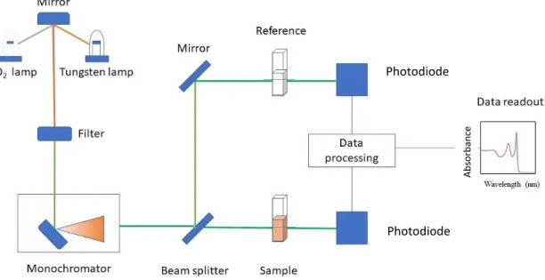
In the experiments, Cary 100 was used as a UV-Vis spectrometer. The general scheme of a UV-Vis spectrometer is shown in Figure 3.1. The working principle can be summarized as follows:
• At first, the light from the lamps (tungsten and deuterium arc lamps) passes through the filter reaching the monochromator where it is separated into different wavelengths,
• Then, the light is divided into two passes by the beam splitter: a part of it goes through the sample cuvette and a part goes through the reference solution usually consisting of pure hexane or toluene,
15
• Finally, the beam passes through the detectors (which are photodiodes in the figure) and the final output showing absorbance vs wavelength (nm) is recorded.
Figure 3.1: General scheme for a typical double-beam UV-Vis spectrometer.
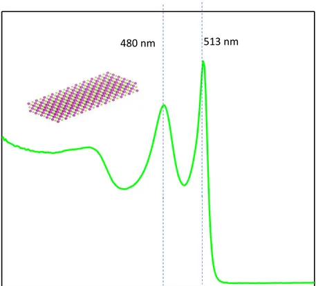
The typical absorption spectrum of 4 ML CdSe NPLs is depicted in Figure 3.2. There are certain electron transitions clearly visible in the spectrum: the electron/heavy-hole transition at around 513 nm (very slight deviation depending on the lateral size) having the lowest photon energy and the electron/light-hole transition at around 480 nm having the highest photon energy value [5].
Photodiode Photodiode A bs o rba nc e
16
513 nm 480 nm
Figure 3.2: Example of absorption spectrum of 4 ML CdSe NPL synthesized at our laboratory showing heavy-hole and light-hole electron transitions.
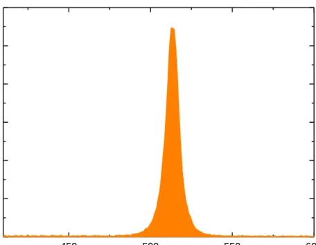
3.1.2. Fluorescence spectroscopy
Another crucial instrument for analysing optical properties of NPLs is the fluorescence spectrophotometer. Fluorescence, by its nature, is a type of the more general concept of photoluminescence. In fluorescence, the singlet excitation occurs where electron preserves its initial spin and it decays faster compared to phosphorescence where emission occurs between any two energy levels that differ in their respective spin states. In this research work as a fluorescence spectrophotometer Cary Eclipse model of Varian company was used. Its main parts consist of a source (typically Xe arc lamp), a sample compartment and a monochromator system which defines excitation and emission wavelengths. Such an instrument, which employs a monochromator system instead of simply filters, is referred to as a spectrofluorometer.
350 400 450 500 550 600 Absor ptivity ( a.u .) Wavelength (nm)
17
A typical PL spectrum of 4 ML CdSe NPLs has a sharp peak at around 513 nm with 6-10 nm full-width at half-maximum (FWHM) at room temperature. This narrow FWHM is unique for NPLs which implies high monodispersity of the synthesized NPLs in their vertical thickness [5], [15], [20].
Figure 3.3: Example of PL emission spectrum of 4 ML CdSe NPL sample synthesized at our laboratory.
3.1.3. Quantum yield measurement
One of the most important factors defining colloidal nanocrystals’ applications is their fluorescence quantum yield (QY). This is defined as the number of emitted photons over the number of absorbed ones. QY is also often referred to as quantum efficiency because it defines the efficiency of conversion of absorbed light to emitted light. QY can be determined in two ways: by absolute measurements using an integrating sphere setup or by relative measurements using the fluorescent standard of a known reference dye [23], [24]. When conducting relative QY measurements, the first step is the choice of an appropriate dye with a similar emission range. Then, the absorbance of the
450 500 550 600 PL In ten sity (a .u. ) Wavelength (nm)
18
reference dye and that of the sample under test are adjusted so that they are similar and below 0.1 absorbance value. As the next step, PL emission is measured and the integrated PL emission is calculated (by integrating the area under the curve). Later, by using the calculated integrated PL emissions of the NPL sample and that of the reference dye based on the already known QY value of the reference dye, the QY of the NPL sample is computed.
To perform absolute QY measurements, the dilute sample is loaded in special cuvettes and placed inside the integrating sphere device. Depending on the emission of the sample, the monochromator is used to adjust excitation created by the light source. Four different spectra are collected in four different configurations: (1) the blank spectrum when the integrating sphere is empty and the light source is open, (2) the sample spectrum when the sample is placed inside the sphere and is excited directly by the light source, (3) the sample is still inside but indirectly excited by the light source, and finally (4) the sample is inside, however, there is no light coming inside. From these four spectra based on the method developed by Mello et al. the absolute QY values are determined [15]. Special attention should be paid for using reasonable concentration values.
3.2. Structural characterization
To analyse shape, size, structure, elemental composition and crystalline structure, various instruments including transmission electron microscope (TEM), x-ray diffractometer (XRD) and x-ray photoelectron spectrometer (XPS) are being used. Obtaining information about the shape and size sheds light on the possible growth of crown and shell layers, while the elemental structure helps to understand more about the growth mechanism and if reactions go each time as planned.
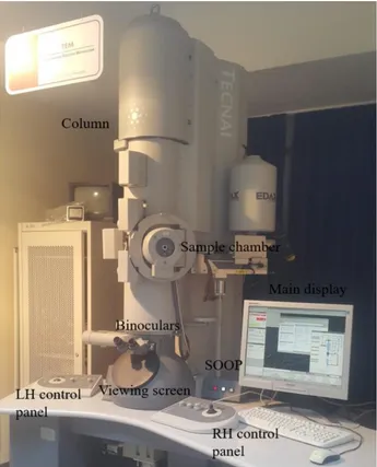
3.2.1. Transmission Electron Microscopy
(TEM)
One of key discoveries for the modern nanoscience was the invention of TEM in 1931 by Ernst Ruska at the University of Berlin, along with Max Knoll. The advantage of electron microscopes over light microscopes is the small de Broglie wavelength of electrons as opposed to light wavelength. This allows images with much higher
19
resolution. Unlike the scanning electron microscopy (SEM) which, primarily, produces images through secondary electrons and electrons back scattered from the surface of the sample, in TEM the images are obtained via information directly collected through the transmitted electrons. Therefore, TEM samples should be thin (typically less than 100 nm). The resolution of TEM is much higher than SEM and can reach 0.1 nm in some modern instruments. Figure 3.4 shows the essential parts of a TEM instrument commonly used in the industry or academia. TEM instruments typically include: a column where the major process is adjusted, left-hand (LH) and right-hand (RH) control panels, binoculars, viewing fluorescent screen, main display and hardware items such as utilities, vacuum pumps, and electronics (Figure 3.4). The column part can further be divided in few crucial parts: an electron gun, condenser lens, a sample stage, objective lenses, objective lens aperture, intermediate lens, project lens, and fluorescent screen (Figure 3.5). Another important feature of conventional TEM hardware is an energy-dispersive X-ray spectrometer (EDS). This is employed for elemental analysis and can be used in dot, line or mapping modes. TEM is constantly cooled with liquid nitrogen while operating and cryo-cycle is turned on whenever it is not used. There are typically three accelerating voltages used: 100 kV, 200 kV and 300 kV.
20
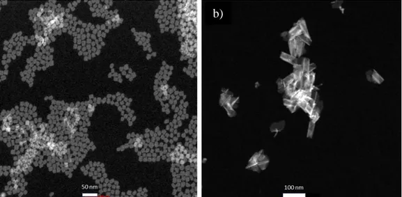
For the structural characterization carried out in this thesis work FEI Tecnai G2 F20 TEM was used. The NPL samples were prepared by first cleaning the liquid sample with ethanol and acetone solvents several times to get rid of the most ligands, which would otherwise burn under the electron beam and make it impossible to focus image for higher magnification and better resolution. Commonly 40-50 µL of the very dilute final solution was dropped on the TEM grid CF300-CU-50 and dried thoroughly. Usually, high-angle annular dark field scanning transmission electron microscopy (HAADF-STEM) mode was used to image NPLs to understand their shape and measure size. The accelerating voltage was usually set to 200 kV. Some typical TEM images of the CdSe and CdS NPLs are depicted in Figure 3.6.
21
Figure 3.6: Examples of HAADF-STEM images of (a) CdSe NPLs and (b) CdS NPLs synthesized at our laboratory.
3.2.2. X-ray powder diffraction
spectroscopy
X-ray diffractometer (XRD) is an essential instrument for analysing crystalline matter, and hence, it is also an important tool for characterization of colloidal semiconductor nanocrystals, especially, NPLs. Though there are numerous types of XRD, the primary one for NPL analyses is an X-ray powder diffractometer often used for procrystalline sample analyses. The idea to use X-rays for analysing crystal structure was generated when Max von Laue discovered in 1912 that substances having crystalline structure rather than amorphous behave as three-dimensional diffraction gratings for X-ray wavelengths because of the equal spacing of planes in a crystal lattice. X-rays are generated by cathode ray tube. Later they are filtered to produce collimated monochromatic radiation and are directed toward the sample. The main working principle of XRD is based on the constructive interference of the X-rays incident onto the crystalline sample. This happens when the Bragg’s condition is satisfied
n*λ=2*d* sin θ (3.2) where n is an integer number, λ is the wavelength, d is the spacing between two planes, and θ is the produced diffraction angle (Figure 3.7).
22
Figure 3.7: A schematic of Bragg’s law working principle.
In our studies, XRD patterns of NPLs were used to prove that indeed the synthesized CdSe/ZnS have the corresponding crystalline structure. The typical zinc-blende (ZB) CdSe NPLs have well-defined XRD spectrum peaks for their (111), (220), (211) and (400) planes (Figure 3.8). Samples were prepared by drying NPLs and dropping the concentrated solution on the corresponding holders.
2 Theta (o)
Figure 3.8: a) XRD spectra of CdSe NPLs, b) XRD instrument.
Incident beam Reflected beam
N o rn ali zed In te n sit y ( a.u .) a) b)
23
3.2.3. X-ray photoelectron spectroscopy
X-ray photoelectron spectrometer (XPS) is one of the useful tools to determine elemental structure and distribution of NPLs. It is a surface sensitive technique meaning it provides information only about the surface structure and to go deeper, one should etch the surface by means of ion gun. The major principal behind the working of XPS is photoelectric effect, which was first proposed by Hertz and later explained by Einstein as a way by means of which light manifests its particle nature. When light is shone on a sample, a photon can be absorbed by an electron and it can escape from the surface with a maximum kinetic energy ofEk=h*ν-EB -e*Ф (3.3)
where ν denotes the photon frequency, EB is electron binding energy and Ф is a work
function, which gives the minimum energy required to remove a delocalised electron from the surface.
The general process has few essential steps. X-ray having energyh*ν is irradiated upon the sample surface to knock out surface electrons. Photons that have more h*ν energy go deeper on the sample surface. Electrons which come from deeper levels are called photoelectrons, they are bound to the core level nucleus with binding energy EB and
the whole phenomenon is referred to as the photoelectric effect. Those generated free electrons possess the kinetic energy Ek after leaving the surface. It is this Ek that is
detected and from that the binding energy EB is calculated.
XPS results are usually used in conjugation with EDS spectra. As the XPS measurements are conducted under ultrahigh vacuum, the samples are dried and placed on special holders very carefully. Any possible contamination of the chamber should be avoided. The obtained spectra are shifted with respect to C s1 binding energy, which has a peak at 284.8 eV.
24
3.3. Aging tests
Though not as widely used as the other characterization methods aging tests are beneficial for understanding potential applications of colloidal nanocrystals including NPLs. They are often used for material quality testing in other fields, particularly industry to understand chemical and mechanical endurance of various materials. NPLs have high surface-to-volume ratio, which leads to rather reduced thermodynamic stability and degradation of optical properties [25][26]. Therefore, in applications which require elevated temperature conditions such as LEDs and lasers understanding thermal stability properties of NPLs is crucial, which can be conducted using various thermal and optical tests.
It is known that PL quenching for QDs happens at elevated temperatures and this leads to decline in optoelectronic features [27]. However, elevated temperature optoelectronic performance of NPLs is one of the critical aspects yet to be studied. To date there has not been much research carried out about it. Probably one of the most significant works was reported by Rowland et al [28], in which CdSe NPLs and CdSe/CdS core/c-ALD shell heteronanoplatelets were examined via static and transient spectroscopies with temperatures ranging from 300 to 700 K under vacuum. Rowland et al. also used in situ TEM which has a feature of temperature control and allows to look at the shape deformations due to temperature elevation. The authors reported that the PL Intensity decreased by about 8-10 times when going from 300 to 400 K, and concluded that it does not depend on the thickness of NPLs or whether there was CdS shell layer. However, the PL Intensity was fully recovered for this range when ambient temperature conditions were restored. Also, unlike QDs, NPLs showed detectable PL Intensity up to higher temperature values. They made a final conclusion that the main culprit behind the PL quenching upon temperature elevation is the PL quenching. Another crucial deduction thanks to TEM images was that morphology remained intact for 4 and 5 ML CdSe up to 560 and 630 K, nevertheless above those values that was deformation cannot be recovered. This was found, in turn, to contribute to the final irreversibility of PL emission. In this thesis work, new approaches were used encompassing both liquid and film thermal tests, as will be presented in the following chapters.
25
4. Shell growths of semiconductor
nanoplatelet heterostructures
4.1. Chemicals
Chemicals used for the synthesis of CdSe NPLs include the following: 1-octadecene (ODE, 90,00 %), selenium (Se, 99,00 %), 1-octanethiol (≥ 98,50 %), zinc acetate (99.99 %), n-hexane (97,00 %), toluene (≥99.90 %), oleylamine (70 %), zinc acetate dihydrate (98 %), ethanol (absolute), oleic acid (OA, 90,00 %), Cd acetate dihydrate (98,00 %), sodium myristate (≥ 99,00 %), Cd nitrate tetrahydrate (≥ 99,00 %), Cd acetate (99.99 %), methanol (99.70 %), Cd acetate monohydrate (99,00 %),N-Methylformamide (NMF, 99.00 %), ammonium sulfide solution ((NH4)2S, 40-48 wt.
% in H2O), acetonitrile (≥99.90 %), sulphur (S, 99,00 %), and acetone (absolute). All
of the substances were acquired from Sigma- Aldrich. No additional purification was applied.
4.2. CdSe core synthesis
The basic steps of the synthesis follow the procedure summarized in Chapter 2.1. However, the size-selective precipitation part is worth mentioning here. First of all, after adding 5 mL n-hexane for better dissolution, centrifugation at 6,000 rpm for 6 min
26
is carried out. The first precipitate mostly consists of unreacted Se and other compounds. Then, the remaining supernatant is divided into 2 parts. After adding 5-6 mL ethanol until the solution became blurry it is centrifuged at 6000 rpm for 6 min. Mostly 4 ML CdSe NPLs precipitate using these particular conditions. However, there still might be a little amount of 3 and 5 ML NPLs, QDs (requires checking with UV-vis and PL spectroscopy) and some OA. Therefore, the sample is kept for one day at the refrigerator. Later, the excess OA, some QDs and 5 ML NPLs are precipitated with 10,000 rpm centrifugation for 3-4 minutes. The precipitate is then disposed of. The hardest part is cleaning 3 ML NPLs, if any present. Some amount of ethanol is added until the liquid becomes very little blurry and it is precipitated at 6,000 rpm. Both the precipitate and the supernatant are checked for the presence of 3 MLs. If necessary, this latter cleaning step is repeated. Nonetheless, with each step more ligands on the surface are detached, and as a result, QY drops and concentration decreases. So, the better reaction goes, the fewer 3 ML NPLs are produced and the higher final quantum and chemical yields are. At the very end, typically, an additional 20 min 10,000 rpm centrifugation is conducted to prevent any non-fluorescent nanoparticles to remain in the final product.
The major modifications are observed in the CdSe NPL depending on the type and amount Cd precursor the shape changes. The shape of the as-synthesized NPLs turned out to be square, rectangular or irregular. This is presumed to be related to the amount water molecules present in Cd acetate, Cd acetate monohydrate and Cd acetate dihydrate precursors [11].
27
a) b) c)
Figure 4.1: HAADF-STEM images of 4 ML NPLs synthesized using a) Cd acetate anhydrate, b) Cd acetate monohydrate, c) Cd acetate dihydrate.
On the other hand, depending on the variation of the amount of Cd acetate dihydrate, the shape can change from square to irregular forms (Figure 4.2, a-d). The major parameter changing here is the amount of water inside the crystal. However, although the NPLs in (d) are near to perfect square, they suffer from diminished chemical yield probably caused by excess Cd acetate. So, in terms of chemical yield, approximately 80-90 mg of Cd acetate is more appropriate under the given conditions. The same kind of experiments were carried out with the addition of pure water but was not successful in having the final square shape.
50 nm nm 50 nm nm 50 nm nm
28
Figure 4.2: HAADF-STEM images showing influence of the Cd acetate amount on the final shapes of CdSe NPLs while all other conditions are kept the same: (a) 90 mg, (b) 100 mg, (c) 110 mg, and (d) 120 mg.
4.3. CdSe/ZnS core/colloidal atomic
layer deposition shell synthesis
One of the techniques of synthesizing colloidal NPL heterostructures, as discussed before, is c-ALD. In the case of CdSe/ZnS core/c-ALD shell NPLs, a synthesis method differing from the typical literature pathway is used, mainly deviating in the chemicals used [19]:
• 1 mL of CdSe core NPL solution was cleaned with ethanol at least 3 times to ensure that surface ligands were torn off ( assumption here is that if 100 µL of CdSe NPLs are diluted by 3 mL of hexane, they have an optical density equal to 1 at 350 nm given the path-length of cuvette to be 1 cm).
29
• The final precipitate was dissolved in 3 mL hexane inside a 50 mL centrifuge tube and 3 mL NMF was subsequently added, which results in two-phase solution.
• In order to guarantee the complete coverage of the surface with S2- ions, the
excess of ammonium sulfide was used – around 100 µL for each semi-layer, which results in transfer of the NPLs from non-polar hexane to polar NMF solution (color change was observed).
• The tube was placed upon a vortex for 5-10 minutes. • Then the upper hexane layer was discarded.
• The precipitation was carried out by adding 0.5 mL acetonitrile and excess toluene and centrifuging for 3 min at 10,000 rpm.
• The process was repeated twice to ensure complete removal of ammonium sulfide and prevent any possible ZnS nanoparticle formation during the subsequent steps.
• The cleaned precipitate of CdSe/S2- was then dissolved in 2 mL NMF and
combined with 2 mL 0.2 M Zn acetate dihydrate solution in NMF.
• After vortexing about 10-15 minutes, the cleaning procedure was conducted twice using toluene as a precipitating agent at 10,000 rpm for 3 min, this concluded the coating of monolayer ZnS.
• For any additional shell layers, the above-mentioned process was repeated. • The NPLs were dispersed in hexane and 0.5 mL of OLA ligand was added. • The sample was heated to promote capping of the surface with the ligand and
was placed to the dark for at least 2 hours.
• Finally, the mixture was cleaned by ethanol at 6,000 rpm and hexane or toluene was added as a dispersant.
30
4.4. CdSe/ZnS core/hot-injection shell
synthesis
One of the most important parts of our CdSe/ZnS project is the implementation of hot-injection shell growth around CdSe NPLs. As discussed in the previous chapters, in c-ALD growth method, although the number of layers can be manipulated easily, it is time-consuming and the synthesized hetero-NPLs, typically, are not chemically stable and do not have high quantum and chemical yield. That is the main motivation for which a new approach is necessary making the hot-injection shell growth a possible better alternative. The most important part is to choose suitable precursors, corresponding temperature range, optimum heating rates and the method of addition of the precursors. One of the most prominent sulphur sources is considered to be 1-octanethiol with the best operating temperature range being 280 – 330 oC. For this reason, the temperature was chosen to be 300oC. For Zn precursor Zn acetate was chosen to be as one of the best options. Below is the main procedure of the synthesis of CdSe/ZnS core/hot-injection shell NPL heterostructures. We developed:
• In a 50 mL round-bottom flask, 5 mL ODE, 36.5 mg Zn acetate (0.2 mmol), a certain amount of the 4 ML CdSe NPL and 500 µL OA were introduced. • As the CdSe NPLs were initially dissolved in hexane, in order to evaporate it,
the solution was kept under vacuum (0.1–0.2 mbar) for about an hour at room temperature (RT).
• OA forms Zn oleate with the Zn acetate and produces water in the process. To remove this water and the remaining volatile chemicals, the flask was heated to around 90 oC and kept at that temperature for 30 min.
• Subsequently, the mixture was switched to Argon gas and 0.5 mL of OLA was added (It was shown before and observed that adding OLA at higher temperatures and long contact of CdSe NPLs with OLA can result in etching. Therefore, OLA was added when starting the reaction at a relatively lower temperature [29]).
31 • The final temperature was set to 300 oC.
• The octanethiol solution prepared beforehand (0.5 mL of 70 µL octanethiol dissolved in 4 ML ODE) was injected dropwise using a syringe pump at the optimum temperature for the first drop being around 170 °C.
• The rate of the syringe pump was set to 10 mL/h at the beginning to ensure to start the growth and was dropped to 4 mL/h at 250 °C to sustain uniform growth on the surface and prevent fume formation at high temperature.
• The reaction for formation of the NPLs with the highest QY value is around 1 hour, which was confirmed experimentally (the results will be shown below). For that reason, the flask was preserved at 300 °C for an hour and then the reaction was quenched by cold water bath and 5 mL of hexane was added to increase dissolution.
• In order to clean the sample from possible side products the centrifugation at 6,000 rpm for 6 min was carried out. No precipitate was observed hinting that possibly no side products were formed.
• Finally, the sample was cleaned with ethanol once at 6,000 rpm for 6 min and was dispersed in hexane or toluene.
All of the above describes the synthesis of CdSe/ZnS thin – shell NPLs. They have 3.04 ± 0.3 nm thickness when the synthesis path described above is followed. However, it is well known that additional shell layers increase chemical stability and possibly QY of QDs [19], [28], [29]. To this end, another method producing thicker shells was used, which employed Zn oleate as one of the Zn precursors. Zn oleate was synthesized according to the literature with some modifications [30]:
• 915 mg Zn acetate (5 mmol), 3.15 mL OA and 16.85 mL ODE were loaded into a 50 mL round-bottom flask and the solution temperature was elevated to 110 oC under vacuum.
• The solution was maintained under this condition to get rid of the formed water, • Later on, the temperature was increased to 150 oC to finalize synthesis of Zn
32
• Before cooling, the final mixture was kept at 100 oC for 10-15 min to evaporate
the possible remnants of water.
• Finally, the solution was preserved at 80 oC under inert gas and used for the
thick-shell NPL synthesis.
The synthesis of the thick-shell NPL, follows a similar route with some variations regarding the additional steps for the growth of the extra layers:
• Similarly, 5 mL ODE, 36.5 mg Zn acetate (0.2 mmol), a certain amount of the 4 ML CdSe NPL and 500 µL OA were loaded to a 50 mL round-bottom flask. • One-hour room-temperature degassing was undertaken to remove possible
hexane left inside.
• To evaporate water possibly formed and hexane possibly left, the temperature was raised to 90 oC and kept there for about 50 min.
• The Schlenk line was then flushed with Argon gas, the temperature was set to 300 oC and 0.5 mL OLA was injected abruptly as soon as the temperature
started to increase.
• As in the previous reaction, a syringe pump was utilized to add dropwise 4 mL ODE and 70 µL octanethiol mixture prepared beforehand inside a glovebox (the rate was 4 mL/h for 30 min).
• Later, Zn oleate solution was introduced into the system in a dropwise manner (special care should be taken when adding with a hot syringe) and 5 min was allowed for the growth.
• The addition of the S precursor was resumed at a 5 mL/h rate.
• After allowing a 40 min period, the reaction was quenched with cold water and 5 mL hexane was injected.
• The cleaning procedure was identical to the thin-shell NPLs yielding almost no side-products.
33
4.5. CdS core synthesis
When it comes to CdS core NPL synthesis, it is harder to control the final shape, as the as-synthesized NPLs tend to fold due to huge lateral dimensions (in contrast to CdSe). Also, even when 4 ML CdS NPLs are synthesized and purified via size-selective precipitation, it is very challenging to achieve pure 4 ML without some tiny amounts of 3 ML and 5 ML CdS NPLs being present. In fact, it is not possible to clean as much as CdSe because ligands are torn away from the surface much easier. The method used in this work for the synthesis is similar to the literature except for some minor modifications [14]:
• 0.1 M of S-ODE precursor was prepared beforehand by heating the corresponding amount of S inside ODE at 120 oC (e.g., for making 20 mL 0.1 M solution, 64 mg of S was dissolved in 20 mL ODE under ambient conditions).
• 217 mg of Cd acetate dihydrate, 2 mL of 0.1 M S-ODE solution, 300 mL of OA and 10 mL of ODE were placed inside a 50 mL round-bottom flask. • Room-temperature Argon bubbling was used as the most efficient way for
removing contaminants for at least 30 mins (in fact, degassing at room temperature results in a low chemical yield of 4 ML NPLs and the percentages of 3 and 5 ML CdS NPLs are higher),
• Then, the temperature was increased to 240-250 oC at a rate of about 23 oC/minute and as the solution reaches the desired value, it is kept there for at
least a minute: the longer the reaction period the bigger the produced lateral sizes.
• Finally, the reaction was quenched by placing carefully in room-temperature water under the flask and injecting 5 mL hexane after the solution reached 120
34
It should be noted that, unlike the previously reported value of 260 oC for the synthesis temperature, when the temperature was kept below 240 oC or above 250 oC 3 and 5 ML CdS NPLs were formed. The deviation may be explained by setting values unique to each heating mental system.
As far as the cleaning process was concerned, ethanol usage was avoided here. Ethanol is more polar compared to acetone. That is why initially weak bonds between CdS semiconductor NPL and carboxylic acid ligands are broken easier with ethanol. As a result, coagulates were formed. Acetone, on the other hand, is weaker, so, chemical and quantum yields are less affected. At first, centrifugation was carried out at 4,000 rpm for 6 min to precipitate contaminants. Some bigger and less stable NPLs were precipitated, as well.
4.6. CdS/CdSe core/crown synthesis
The recipe used for CdS/CdSe core/crown heteronanoplatelets synthesis differs from the literature [31]. There are two different Se precursors used: ODE-Se and TOP-Se. For the preparation of 0.1 M ODE-Se solution, 15 mL ODE and 118.5 mg Se were loaded to a 50 mL flask. It was degassed for 1-2 min and then switched to Argon gas. It was heated to 90 oC and kept at it for 1 hour. Then the temperature was raised to 120
oC and maintained there for half an hour. Subsequently, it was kept at 150 oC and then
180 oC for half an hour each. It was cooled and kept for later usage. To make 0.1 M TOP-Se solution, 0.1 mmol of Se was added to 1 mL TOP inside a glovebox because TOP is flammable in air. It was mixed at 50 oC to dissolve faster. Cd precursor was also made separately beforehand as described in CdSe/CdTe core/crown synthesis in Chapter 2.2. After producing necessary precursors and synthesizing CdS NPLs the following steps were implemented:
• CdS NPLs (amount equalling to 0.5-1 O.D.), a certain amount of crown precursors (typically 500 µL), a little amount of OA (usually between 50-75 µL) and 5 mL ODE were added to a 50 mL round-bottom flask.
35
• The mixture was degassed at room-temperature for at least 1 hour to remove any hexane and contaminant volatile substances, which might be present. Then it was degassed at 90 oC for 20-25 min.
• Meanwhile, TOP-Se solution was prepared for injection with a syringe pump: inside the glovebox, 60 µL of 0.1 M TOP-Se solution was mixed with 2 mL ODE and 0.5 mL of it was taken by a 20 mL syringe avoiding any bubbles inside.
• The system of the reaction was changed to Argon gas and temperature was set to 240 oC.
• The first drop of Se precursor was set to be around 180 oC and the rate was 8
mL/h.
• The reaction vessel was kept at 240 oC for about 8-10 min.
• Then the reaction was quenched by cold water bath and 5 mL of hexane was poured for better dissolution.
• The cleaning was performed by using both acetone and ethanol after the first precipitate was disposed of by 2,000 rpm centrifugation.
Depending on the quantity of Cd crown precursor employed and time period of the reaction, the formed core/crown structure may become more red-shifted. Better results were obtained when TOP-Se precursor was used instead of ODE-Se. This can be caused by better dissolution of Se inside TOP and its assistance when attaching to CdS NPL surface.