by Hilal Kızılcabel
Submitted to the Institute of Graduate Studies in Science and Engineering in partial fulfillment of
the requirements for the degree of Master of Science
in
Electrical and Electronics Engineering
Bilgi University 2017
MICROMACHINED PLATFORM DESIGN FOR ALL-OPTICAL MICROSYSTEMS
APPROVED BY:
Assist. Prof. Dr. Baykal SARIOĞLU ………...
(Supervisor)
Assist. Prof. Dr. Yiğit Dağhan GÖKDEL ………
(Co-Supervisor)
Assist. Prof. Dr. Okan Zafer BATUR ………...
Assist. Prof. Dr. Yeşim ÖNİZ ………...
Assist. Prof. Dr. Onur FERHANOĞLU ………...
(İstanbul Technical University)
ACKNOWLEDGEMENTS
Thanks to the support of so many people in the process of writing the thesis, I have motivated every time.
First of all, I would like to thank my supervisors, Asst. Prof. Baykal Sarıoğlu and Asst. Prof. Yiğit Dağhan Gökdel for their guide and encouragement throughout the duration of the work. I feel myself lucky to be their student and colleague. I would say sincerely that theirs support in every way. This work would not have been completed without their support. In addition, I would also like to acknowledge Asst. Prof. Okan Zafer Batur, Asst. Prof. Yeşim Öniz, and Asst. Prof. Onur Ferhanoğlu for attending on my thesis committee.
Special thanks to my dearest friend Ahmet Uğur Dilek for his helpful. His presence has given me strength of both my life and academic life. If it was not for his support, this thesis could not have been possible.
I would also like to thank Ahmet Tuna. We have always been support and patient with each other during our work. I am a member of Microsystems Lab., since my bachelor of science and during my master thesis. I also thank you to my lab mates for the great atmosphere.
I would like to thank TUBITAK Project No’s: 114E549. In addition, I would like to thank Boğaziçi University Clean Room team for helping me with this work. Also, many thanks go to Boğaziçi University EEEN department for the chip we're working on.
I would like to present my special thanks to which is the most precious people in my life, my mother, Hülya Kızılcabel and my father, Zafer Kızılcabel. I am grateful them for believing and always being patient and supportive of me. I also thank them for endless love.
Last but not least, I want to thank endless to a person, my little brother Kıvanç Kızılcabel who is my real power throughout my life and he is also the perfect gift and love for me.
ABSTRACT
MICROMACHINED PLATFORM DESIGN
FOR ALL OPTICAL MICROSYSTEMS
Nowadays, people use at least one of the electronic devices in daily life and these devices need power. This power need causes many problems such as cost, time and effort. These kinds of problems are not an essential issue for non-vital uses, but in a medical environment it has an important place. Biomedical microsystems are implanted in-vivo application. When the devices use as this purpose, it must be designed for fit in to human body.
Microsystems provides more efficient results with optical methods; safe, low area and low cost against the problems encountered in applications using radio frequency transmitted and external non-rechargeable batteries.
In this study, the micromachined platform is designed to be compatible with microsystems and to be easily installed, in order to ensure optimum combined performance of optically operating microsystems. The proposed platform is printed using additive manufacturing fusing (3D printed) technology. Thanks to this method, the micromachined platform is designed to have the desired dimensions and more economical, lighter and more portable. The optical microsystems provide an ideal performance through the micromachined platform.
Keywords: Micromachined platform, 3D printed technology, Optical microsystems, Optical fiber transmission, CMOS photodiode.
ÖZET
OPTİK MİKRO SİSTEMLER İÇİN
MİKRO PLATFORM TASARIMI
Günümüzde insanlar günlük yaşamlarında elektronik cihazlardan en az birini kullanmaktadır. Bu cihazlar yaşam kalitesini artırmasının yanı sıra çalışması için gereken güce ihtiyaç duyması maliyet, zaman ve emek gibi birçok probleme neden olmaktadır. Bu tür sorunlar hayati olmayan kullanımlar için çok önemli bir mesele değildir, ancak medikal bir ortamda önemli bir yere sahip olmaktadır.
Biyomedikal uygulamalarda mikro sistemler insan vücuduna uygulanır. Sinyalin radyo frekans ile iletildiği veya harici şarj edilemeyen pillerin kullanıldığı uygulamalarda karşılaşılan problemlere karşı; optik yöntemler, daha güvenli, düşük alana ve düşük maliyete sahip bir mikro sistem sağladığı için, optik yöntemlere dayalı çalışmalar ile daha verimli sonuçlar elde edilmektedir.
Bu çalışmada, optik olarak çalışan mikro sistemlerin, optimum kombine performansı sağlaması için, mikro sistemlerle uyumlu ve kurulumunun kolaylıkla yapılabileceği bir mikro platform tasarlanmıştır. Önerilen platform 3D yazıcı imalatıyla yapılmış olup, bu yöntem sayesinde mikro platform istenilen ölçülerde tasarlanıp; ekonomik, daha hafif ve taşınılabilir bir ürün oluşturulmuştur. Böylece, platform yardımıyla optik olarak güç sağlayan mikro sistemlerde ideal bir performans sağlanmaktadır.
Anahtar Kelimeler: Mikro platform, 3D yazıcı teknolojisi, optik mikro sistemler, optik fiber iletimi, CMOS foto diyot.
TABLE OF CONTENTS
ACKNOWLEDGEMENTS ... iii
ABSTRACT ... iv
ÖZET ... v
LIST OF FIGURES ... viii
LIST OF TABLES ... xi
LIST OF ABBREVIATION / SYMBOLS ... xii
1. INTRODUCTION ... 1
2. SYSTEM DESCRIPTION ... 5
2.1. OPTICAL POWER SOURCE ... 7
2.2. OPTICAL FIBER ... 9
2.2.1. Basic structure of an optical fiber ... 10
2.2.2 Types of Fiber Modes ... 11
3. PROPOSED DESIGN ... 14
3.1. ALIGNED THE SYSTEM ... 14
3.2. MECHANICAL STRUCTURE ... 16 4. FABRICATION ... 22 4.1. 3D PRINTING TECHNOLOGIES ... 22 4.2. FABRICATION TECHNIQUE ... 23 4.2.1. 3D Printing ... 23 4.2.2. Polishing ... 25 5. EXPERIMENTAL RESULTS ... 27 5.1. EXPERIMENT SETUP ... 27
5.1.1. Experimental Setup of Testing Fiber Cable ... 27
5.1.2. Experimental Setup for Testing Micromachined Platform ... 32
6. CONCLUSIONS & FUTURE WORK ... 42 APPENDIX A: CAD DRAWING OF THE DIMENSIONS OF THE PLATFORM .. 44 APPENDIX B: CALCULATION OF THE LOCATION OF THE DETECTOR ... 45 REFERENCES ... 46
LIST OF FIGURES
Figure 1.1. Wireless implantable medical devices [3] ... 1
Figure 1.2. A fiber-optical cable butt-coupled to an IC [15], (b) Sketch of the physical realization of the integrated system [1] and (c) Integration of CMOS Photodiodes with fiber lines [1] ... 3
Figure 2.1. System schematic of the microsystem ... 5
Figure 2.2. CAD drawing of operation system ... 6
Figure 2.3. The configuration of the photodiode structure [20] ... 7
Figure 2.4. Micrograph of the CMOS chip (left), Layout view of the power photodiode (right) ... 8
Figure 2.5. I–V curves obtained at different laser powers for PPD [19] ... 8
Figure 2.6. (a) The fabricated chip (b) which placed on ceramic leadless chip carrier package ... 9
Figure 2.7. The structure of a typical fiber [23] ... 10
Figure 2.8. Schematics of single mode fiber ... 11
Figure 2.9. Schematics of step index multi mode fiber ... 13
Figure 2.10. Schematics of graded index multi mode fiber ... 13
Figure 3.1. Locations of system parts ... 14
Figure 3.2. (a) Ceramic Leadless Chip Carrier Package and (b) socket (LCC-044) [26] .... 15
Figure 3.3. Soldering the package on PCB ... 15
Figure 3.4. CAD drawing of; (a) socket and (b) proposed micromachined platform ... 16
Figure 3.5. CAD the proposed micromachined platform; (a) with the fiber path and (b) the cover ... 17
Figure 3.6. CAD drawing of V-shaped groove ... 17
Figure 3.7. CAD drawing of V-shaped groove ... 18
Figure 3.8. CAD drawing of (a) the cover both top and bottom view and (b) the micromachined platform with its cover ... 18
Figure 3.9. CAD the proposed micromachined platform; with the column ... 19
Figure 3.10. View of aligned all parts ... 19
Figure 3.11. CAD simulation of travelling fiber into micromachined platform ... 20
Figure 4.1. The object first become more recognizable (a) at the end of the print process,
(b) it is completed object [27] ... 22
Figure 4.2. 3D-printed the micromachined platform; (a) CAD drawing of the designed platform structure and (b) the manufactured platform ... 24
Figure 4.3. 3D-printed the cover of micromachined platform; (a) CAD drawing of the designed cover of platform structure and (b) the manufactured cover of platform ... 24
Figure 4.4. 3D-printed the micromachined platform; (a) CAD drawing and microscope image, (b) its reflective surface and (c) its fiber path ... 25
Figure 4.5. (a) Before manufactured the micromachined platform and (b) after processing ... 26
Figure 4.6. (a) Before manufactured the micromachined platform and (b) after processing for the cover ... 26
Figure 5.1. (a) Laser diode mount, (b) input pins of laser diode and (c) mounted diode on breadboard ... 28
Figure 5.2. (a) Example of fiber, (b) closed up of mounted pigtail ... 28
Figure 5.3. Normalized output power vs. forward for laser diode [29] ... 29
Figure 5.4. Experimental setup to find out the power of the fibers ... 29
Figure 5.5. The comparison power of different pigtails ... 30
Figure 5.6. Experimental setup to find out the power of the fibers; while the output voltage closed ... 31
Figure 5.7. Experimental setup to find out the strong power of the fibers; while the output voltage given to 2.0 V ... 31
Figure 5.8. The micromachined platform; (a) top view of socket, (b) view of coating ... 32
Figure 5.9. View of the mold ... 33
Figure 5.10. Measured the angle of reflective surface ... 33
Figure 5.11. (a) sticky reflective marker, (b) stick on fabricated micromachined platform 34 Figure 5.12. Experimental setup to measure the power of the fiber by using multimeter on the produced micromachined platform ... 34
Figure 5.13. View of the micromachined platform ... 35
Figure 5.14. Curves obtained of optical power coupling for selected fiber ... 35
Figure 5.15. Photodiode output pins ... 36
Figure 5.17. Experimental setup to measure the power of the fiber using multimeter on the
produced micromachined platform; while the output voltage closed ... 37
Figure 5.18. Experimental setup to measure the power of the fiber using multimeter on the produced micromachined platform; while the output voltage given to 2.0 V ... 37
Figure 5.19. Experimental setup to using the function generator to analyze the power ... 39
Figure 5.20. Display of a 10.000 Hz square wave from a function generator ... 39
LIST OF TABLES
Table 3.1. Depicted in items ... 14 Table 4.1. 3D-printed the micromachined platform; production estimation and printing mode section ... 24 Table 5.1. Depicted in values ... 40
LIST OF ABBREVIATION / SYMBOLS
MEMS Micro Electro Mechanical Systems
EMI Electromagnetic Interference
RF Radio Frequency
OWC Optical Wireless Communication
Li-Fi Light Fidelity
Wi-Fi Wireless Accuracy
LED Light Emitting Diodes
VLC Visible Light Communication
PPD Power Photodiode
TIR Total Internal Reflection
NA Numerical Aperture
UV Ultraviolet
CAD Computer Aided Design
SMT Surface Mounted Diode
STL Stereolithography
3D / 2D Three Dimensional / Two Dimensional
PCB Printed Circuit Board
SLA Stereolithography
DLP Digital Light Processing
FDM Fused Deposition Modeling
SLS Selective Laser Sintering
SLM Selective Laser Melting
EBM Electronic Beam Melting
LOM Laminated Object Manufacturing
PMMA Polymethyl Methacrylate
k Extinction Coefficient 𝑛 Refractive Index ɸ Reflection Phase ϵ Relative Permittivity R Reflectance A Ampere V Volt dB Decibels
1.
INTRODUCTION
Electronic devices are used in the biomedical area for the health applications. Recent studies have shown that wireless biomedical microsystem designs with low power consumption and small footprint will be implanted in-vivo and are used for recording health data of patients. Thus, implanted devices are monitored without affecting the daily life of the patient and necessary preventions are taken.
Some applications such as pacemakers, cochlear implants, the contact lenses with a Microelectromechanical Systems (MEMS) are applied to Radio Frequency (RF) and non-rechargeable batteries. Although these applications result in significant progress in human health, the power consumption becomes a very essential disadvantage. Non-rechargeable batteries or radio frequency (RF) signals, provide wireless energy for the medical devices [1-2]. Non-rechargeable batteries require renewal when they are depleted. This can increase the cost and it can also decrease the life quality of the patient.
Figure 1.1. Wireless implantable medical devices [3]
On the other hand, the RF signal power is transmitted via an RF antenna. This antenna covers a large microsystem area. Alternative methods are required for finding solutions to such problems.
There are several areas of application with the inclusion of wireless communication and medical imaging, which make electrical systems to high RF fields, magnetic fields, electromagnetic interference (EMI) [4], or high temperature medium. It is more convenient to provide the power of these systems through optical, rather than electrical means [1,5-7].
Power consumption solutions were also developed with the integrated circuit technology. Apart from the local battery or RF power, “optical methods” are a very efficient way to consume power. The main purpose of using optical power is to reduce the number of conductive lines into the system and at the same time to help abolish the Ohmic losses and the heating effects, for example strong RF fields [1].
In the literature, it is shown that fiber optic cables can be used for signal transmission in a relatively immune environment to RF excitation, an optic using components such as light emitting diodes and lasers. Optical signal transmission uses specially designed receiver and transmitter [8-9].
The designed wireless biomedical microsystems prevent the problems in existing applications by using optical methods. These microsystems use optically supplied power. Thus, there is no need for extra area in designed microsystems (for an external battery, etc…). Both of the cases mentioned the above consume more large areas. Thus, biomedical implant [2,10-13], retinal prosthesis devices and sensors [14] require a space-efficient monolithic approach in the case of direct integration of a single chip photodiode into the electronic circuitry as mentioned in the literature [15-18].
In this study, designed microsystems was used microsystem for biomedical application. The devised microsystem was developed to be optically amplified and optically programmable for preventing problems with applications such as non-rechargeable batteries or RF power. Microsystems designed by using optical methods do not affect daily life without causing damage to the patient. This optic method avoids consumption of area, cost, etc... in contrast to other applications.
In the light of all these mentioned above, the devised microsystems can be easily operated with an optical method, so it can be said that a specially designed micromachined platform design is needed. The designed platform will be immobilized the fiber cable.
The main purpose of the proposed platform is to transfer the light from the laser source with fiber optical to the photodiode with optimum combined performance without losing efficiency and to operate the microsystem with optical power. The microsystem is coupled with a package during manufacturing process. This package is detailed in Chapter 3.1.
In the literature, one method is that fiber-optical cable is butt-coupled to the microsystem by fixing the fiber position [15]. Another method, the fiber is held or attach onto the microsystems in other words chip package. [1]. But these methods are not very useful because not being fixed on the chip package. In the proposed, the dimensions of the designed micromachined platform is the same as the chip package, so it can be installed easily. Hence, the chip and the micromachined platform integration is ensured.
Figure 1.2. A fiber-optical cable butt-coupled to an IC [15], (b) Sketch of the physical realization of the integrated system [1] and (c) Integration of CMOS Photodiodes with fiber lines [1]
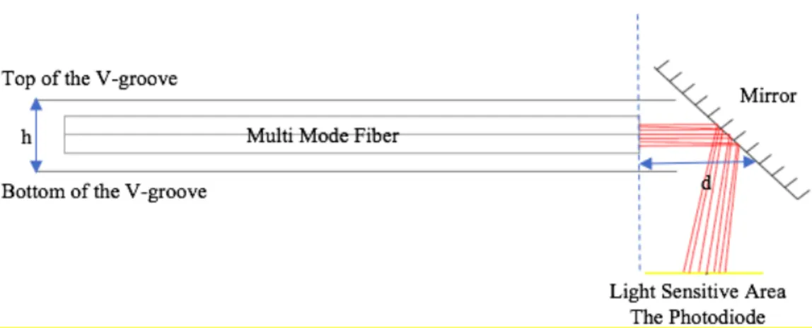
The designed micromachined platform completely covers the chip package. Only where the bottom of the micromachined platform has an aperture to the photodiode for receive light. This aperture is at the end of the specially designed fiber path which has V-shaped groove. 125 µm core fiber with a wavelength of 850 nm places in this groove. The light reaches to the light sensitive area, where the photodiode of the chip is going to be aligned, receives the light reflected from designed curved surface at end of the fiber path. In order to have the reflection properties of this surface, it is covered with reflective marker. The fiber which is driven by the laser diode is traveling on the platform and reflected on the reflective surface and then collects on the photodiode. This process is in detail Chapter 5.1.
The micromachined platform was printed with the help of 3-Dimension (3D) printed technology by using AutoCAD software. This technology is mentioned in detail Chapter 4.1. and Chapter 4.2. A transparent material named VeroClear was selected for the production of the micromachined platform. Subsequently, specific areas (inside and outside) were covered according to the application.
2.
SYSTEM DESCRIPTION
The main aim of the used microsystem takes power optically and programmed optically. There is no need for an RF power [1-2] and an antenna for data transmission for the proposed system, since optical transmission methods are utilized. Thus, this application has an advantage in low area consumption.
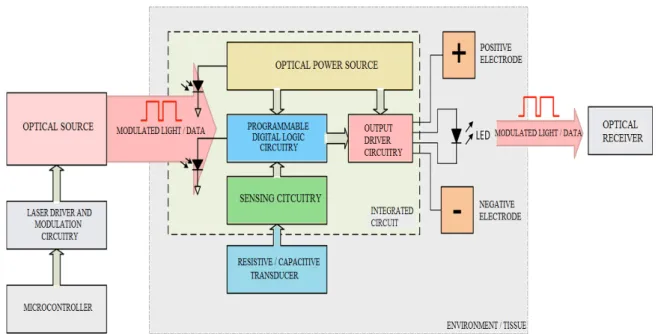
A capacitive or resistive transducer is used in the proposed microsystem. The micro system collects the patients’ data from the tissue or environment. The collected data has impedance values and sends them to the sensing circuit via summation transforms. Thereafter, the sensing circuit transforms transfer the impedance values into electrical and processable signals. Signals conduct to the programmable digital circuit. A patient's health condition can be monitored remotely, without damage or by not affecting the daily life of the patient and during the monitoring process, remote intervention mode was applied where necessary. Electrical signals with voltage values on positive and negative electrodes are applied to the intervention mode [1,15,19]. In addition, these signals can be transferred for monitoring by way of a LED [15] for the monitoring mode. The system diagram of the optical power supply presented is shown in Figure 2.1.
The optical power supply unit converts the power of an existing external laser into electrical power and sends it to the electrical components of the receiver [1,15]. Therefore, the operation of the microsystem which is optically powered and optically programmable provide.
In this study, the main aim is preventing the escape of light and getting the best performance. Since the proposed micromachined platform will be placed on the micro system, an opening is created on the platform to reach the laser on the light sensitive area. An external laser which a multimode with a wavelength of 850 nm is used. Therefore, the laser directly travels onto the light sensitive area. It collects the power from the external laser and supplies it to the electronic components of the integrated device. Also, the power and data transmission are achieved with a single channel in microsystems. The operation system of the proposed platform presented is shown in Fig 2.2.
Figure 2.2. CAD drawing of operation system
Consequently, the proposed micromachined platform is aligned onto the microsystem so that the light sensitive area (photodiode) have the optimum combined performance for all optical microsystems.
2.1. OPTICAL POWER SOURCE
There are different modes of power transmission. These are referred as intermittent and continuous modes. The intermittent mode provides some energy accumulation of the source and to transmit it later. Power can be transmitted in greater amounts at this stage. On the other hand, the continuous mode is simpler that has a more stable output. The aim of the system is run the continuous mode [19-20].
The microsystem itself is formed of two main elements. The power photodiode (PPD) converts the optical power to electrical power before its anode voltage is boosted by the dc/dc converter unit. Power required for the dc/dc converter and other elements of the source is provided by the PPD as well [15,19-20].
If the system is in intermittent mode, both photodiodes need to be illuminated. It is not useful to use multiple light sources and waveguide for this. Using a single laser driver for both photodiodes means that during an intermittent process the power photodiode and dc/dc converter compound cannot be active.
Figure 2.3. The configuration of the photodiode structure [20]
Since the photodiode would be used in photovoltaic mode, its anode voltage is of interest, whereas CMOS configuration would require the p-substrate to be grounded to prevent MOSFET leakage current to the substrate. This means the photodiodes have to employ p-well region as their anodes. Consequently, both photodiodes use junctions based formed by
the p-well and deep n-well. The cathode is grounded shorted to a substrate to eliminate the parasitic p-substrate/n-well junction shown in Figure 2.2. [1,19-20].
Figure 2.4. Micrograph of the CMOS chip (left), Layout view of the power photodiode (right)
The photodiode driver was designed which is a part of this project. This photodiode driver increases the digital high to supply voltage. When the intensity of light decreased, the saturation process of the photodiode was not occurring in an instant. Therefore, since the light intensity changes, and can reach the 0.65-0.7 V under the high-intensity light. For the optical power source, the used photodiode is shown in Figure 2.4. in this microsystem.
However, the supply voltage can be wanted to increase under the low-intensity light situations. Therefore, dc/dc converter is used that an amplifier increases the DC voltage. In microsystems have the storage capacitor that at the output of the dc/dc converter. This capacitor accumulates electrical charge when the load is inactive in intermittent mode; whereas it reduces output ripple significantly in continuous mode [19]. This mode configuration keeps this switch shorted at all times. An external storage capacitor [1,15,19-21] was added on the microsystem when taking into account all of these. The capacitor is designed externally with a reason that the micro system is small.
The photodiode will provide its power by the laser source. Hence, the fiber with a wavelength of 850 nm was used which is focused onto the chip photodiodes, the photodiodes attendantly supply the ideal performance.
Figure 2.6. (a) The fabricated chip (b) which placed on ceramic leadless chip carrier package
2.2. OPTICAL FIBER
Optical fiber is often used in light guide or data transmission implementation. The fiber optic applies to the medium by means of information transmission in the form of a glass or plastic wire or a light pulse along the fiber. Used in light guide applications, the optical fiber is a safe, heat-dissipative light transmission ideal for medical, inspection, automotive or display applications [22].
2.2.1. Basic structure of an optical fiber
Optical fibers are circular dielectric waveguides that can carry optical energy and information. Their a central core is surrounded by a concentric cladding with slightly lower (by ≈ 1%) refractive index [23]. Its function is to direct visible and infrared light to long distances. In the form of silicon dioxide consists of a glass core, the light breaks less than itself. This material has a crystalline form of a semiconductor structure. An optical fiber is to guide light along its length by limiting as much light as possible in a spreading form. An optical fiber transmission of light depends on preventing light from escaping from the fiber.
A principle called total internal reflection allows fiber optics to take the light they carry. Light occurs when a critical angle illuminates the boundary between material and a greater angle. The basic structure of an optical fiber consists of three parts. These are the core, the cladding, and the coating. The basic structure of an optical fiber is shown in Figure 2.7. [23].
Figure 2.7. The structure of a typical fiber [23]
The core is a cylindrical rod of very thin size dielectric material. Dielectric material conducts no electricity. It carries the light from the transmitter to the receiver. The core diameter can change from about 5 µm to 100 µm [24]. The core is surrounded by a layer of material called the cladding. It tries to keep the light in the core along the total internal reflection. The index of refraction of the core material is much than that of the cladding material. The cladding provides some functions. The cladding performs the functions respectively. It reduces a loss of light from the core into the surrounding air and scattering loss at the surface of the core.
Coating preserves the fiber from absorbing surface contaminant; it adds mechanical strength. The standard diameter of fiber after the coating is about 250 µm to 300 µm [24].
2.2.2 Types of Fiber Modes
Optical fiber based on several modes of propagation is classified into two types. As it is mentioned before, calculated are made of modes.
2.2.2.1. Single Mode Fiber
Figure 2.8. Schematics of single mode fiber
In single mode fiber, only one mode can spread through the fiber. The light is passed through the single mode fiber through laser diode. Single mode fiber has higher bandwidth and lower attenuation [23].
The fiber cannot be modeled using geometric optics having a core diameter less than about ten times the wavelength of spreading light. Instead, the solution of Maxwell’s equations reduced to the electromagnetic wave equation should be analyzed as an electromagnetic structure [25]. The fiber supports one or more limited transverse modes in which the light can be propagated through the fiber.
Fiber has small core diameter (5µm), and high cladding diameter (70µm) and the difference between the refractive index of core and cladding is very small. There is no dispersion and degradation of the signal during traveling through the fiber [23].
2.2.2.2. Multi-Mode Fiber
Multimode fiber allows a large number of modes for the light ray traveling through it. It has lower bandwidth and high attenuation according to single mode fiber.
The core diameter of fiber can be analyzed by geometrical optics. Rays that reach the core and cladding boundary at a high angle boundary are completely reflected. However, rays that reach the boundary at a small angle are refracted from the core into the cladding.
The core diameter is 62.5µm, and that of the wavelength is 850-1300nm. It is transmitted infrared laser light. It reduces the cost of production and but higher a number of losses according to single mode [23].
The refractive index difference is also larger than single mode fiber. There are two types of multimode fiber based on the refractive index.
2.2.2.2.1. Step Index Multi Mode
It is similar to single mode fiber. The only difference is that its central core is much wider. It has a wider fiber aperture. This provides more light to the cable.
The lights that strike at a larger angle from the critical angle between core and clad propagate in the form of hand they are constantly reflected off the boundary. Otherwise, the rays that multiply with a smaller angle from critical angle disappear. The light enters the clad. Light can find many ways that can follow. As a result of this, they do not follow the same path. Therefore, they do not travel at the same time from one end of the fiber to the other end.
Figure 2.9. Schematics of step index multi mode fiber
2.2.2.2.2. Graded Index Multi Mode
The index of the core changes depending on the radius. The light is spread out from the inside out as concentric circles. The refractive index of each ring is different. The largest index at the center, and the smallest index at the outermost.
The direct light to the center is a short way. But in here the index is big. Another, the outgoing light is a long way. But, since the index is small, the speed of the light varies inversely with the index profile. Therefore, all lights converge at certain node points.
3.
PROPOSED DESIGN
The proposed design consists of two parts. In the first part is aligned the system is presented dimensions. Second part is mechanical structure of the design is mentioned which refers to the parts of design of the design. The reason and how the design is designed is explained in the second part.
3.1. ALIGNED THE SYSTEM
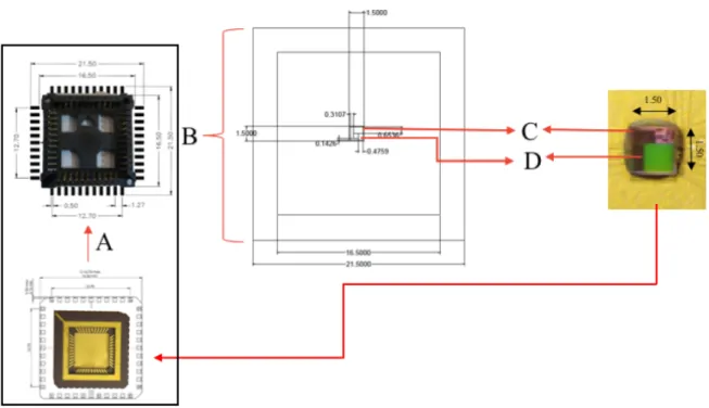
Figure 3.1. Locations of system parts Table 3.1. Depicted in items
A Ceramic Leadless Chip Carrier Package [16.50x16.50 mm2] B SMD Type – Socket 44pin [21.50x21.50 mm2]
C The Chip (IC Design) [1.5x1.5 mm2] D The Photodiode
Figure 3.2. (a) Ceramic Leadless Chip Carrier Package and (b) socket (LCC-044) [26]
The chip is fabricated 1.5(width) x 1.5(length)mm on the ceramic leadless chip carrier package (IC-LCC socket) [26] which can be shown in the Figure 3.2. This package has an area of 16.50 x 16.50 mm and 44 pins. SMD type of the socket (LCC-044-H403-55) [26] is preferred to make solder more comfortable on printed circuit board (PCB) given in the Figure 3.3. The package dimensions and features are described shown in Figure 3.1 and Table 3.1.
The micromachined platform has been planned according to the size of the socket and the chip and their location as specified in the technical drawing. Since the micromachined platform will be placed onto the socket, it has been designed minimum 21.50(width) x 21.50(length) mm.
3.2. MECHANICAL STRUCTURE
AutoCAD is a mechanical design software. The micromachined platform has been created easily by using it.
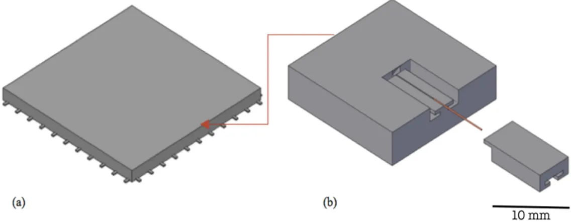
Firstly, as shown in Figure 3.4., proposed platform placed onto socket. Since the microsystem on socket is under the platform, an opening is created just above microsystem on the platform. This way, the laser beams reach onto light sensitive area. Dimension of opening is same as dimension of microsystem so is 1.5 mm x 1.5 mm.
Figure 3.4. CAD drawing of; (a) socket and (b) proposed micromachined platform
The micromachined platform is composed of four parts namely fiber path, cover, column and reflective surface which are shown in Figure 3.7., Figure 3.8 and Figure 3.9. and red part is also fiber.
Figure 3.5. CAD the proposed micromachined platform; (a) with the fiber path and (b) the cover
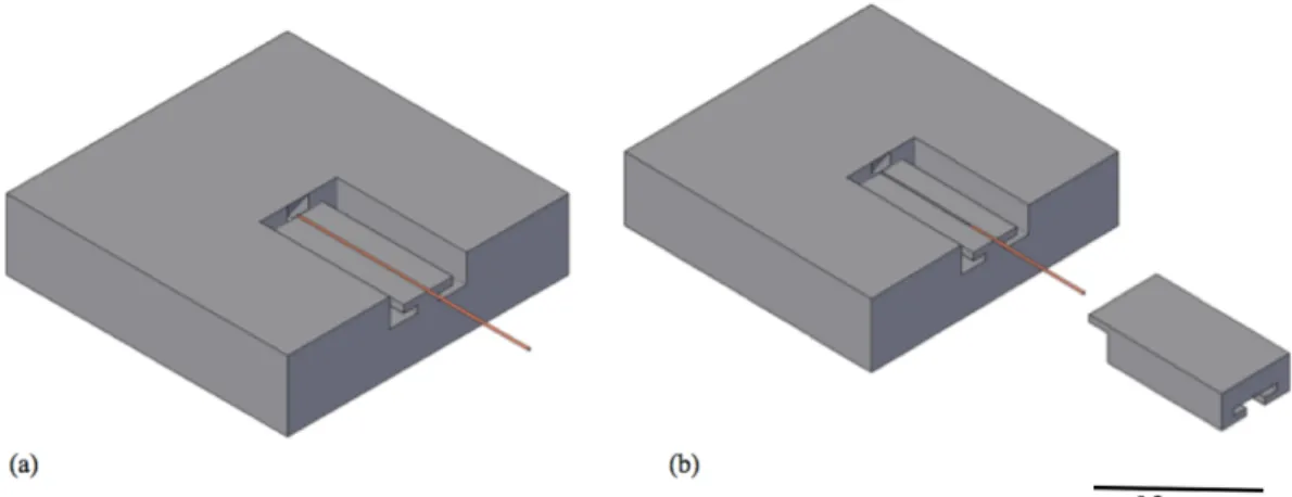
Alkaline etching of crystalline using KOH (potassium hydroxide) is performed for creating various feature definition in MEMS. The alkaline chemistries have the ability to preferably etch silicon along the crystal processing. This makes it possible to create geometries difficult to produce with other micromachining techniques (for example V-grooves) [27]. Silicon nitride V-shaped grooves fabricated with MEMS technology are passive structures to use for the alignment of components in optical fibers.
In order to make a comparison with the study done by silicon etching [1], this designed platform was designed in V-shape. So that, making the fiber path as V- shaped groove has been created according to dimension of selected fiber as shown in Figure 3.6. The diameter of the multimode fiber as 2r = ∅125 µm. Fiber will put this groove. Thus, it prevents from fiber from moving. The length of the fiber path is up to the point where the microsystem starts and this path is also approximately 11.65 mm as is seen from Figure 3.7.
Figure 3.6. CAD drawing of V-shaped groove
Figure 3.7. CAD drawing of V-shaped groove
Secondly, the cover has been created along the fiber path and designed L-shaped as shown is Figure 3.8. (a). It provides;
1. It does not allow light to pass from outside to inside 2. It makes easy to follow the fiber.
It can be seen in Figure 3.8 (b).
Figure 3.8. CAD drawing of (a) the cover both top and bottom view and (b) the micromachined platform with its cover
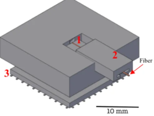
Third part is the columns at the four corners under the micromachined platform has been designed is shown in Figure 3.9. When the platform put on pins of the socket, columns prevent it from moving on pins.
Figure 3.9. CAD the proposed micromachined platform; with the column
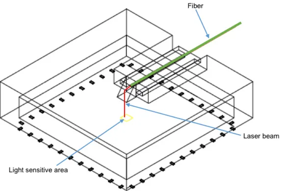
All mentioned parts are aligned as in Figure 3.10. It shows fiber path, cover, and alignment of columns with socket according to the series number.
Figure 3.10. View of aligned all parts
Since the microsystem is under the platform, there is a necessity surface for reaching light to the light sensitive area. So, a surface which inclined structure and an angle of 54.7° has created in the platform. It shown in Figure 3.11. This surface allows to reach light to desire location.
Figure 3.11. CAD simulation of travelling fiber into micromachined platform
As it is explained before, to make a comparison with fabricated silicon-based [1], the angle of inclined surface is 54.7° In studies, silicon etching made using KOH and silicon etches anisotropically with a 54.7° angle from the plane [27].
Figure 3.12. CAD simulation of travelling fiber into micromachined platform
Design parameters of the micromachined platform are depth (h) of the V-shape groove, radius (r) of fiber, the width of the opening and the separation between the fiber end to the reflective surface (d). As it is mentioned before, the width of the opening (d) is approximately the same as the size of microsystem that is 1.5 x 1.5 mm.
The numerical aperture of the fiber defines the reflective surface size and the separation between the reflective surface and the fiber. The micromachined platform has been designed diameter of the multimode fiber as 2r = ∅125 µm, and numerical aperture as 0.10 - 0.14. The numerical aperture of the fiber corresponds to an aperture angle of
The inclined surface acts as mirror after the specific processes for reflecting. Thus, the lights travel through fiber, then they scatter from this surface and reflect onto photodiode in same time.
4.
FABRICATION
The applications required for the manufacture steps for the proposed design are elaborated.
4.1. 3D PRINTING TECHNOLOGIES
The use of 3D (three-dimensional) printers has increased with advancing technology, and it is very popular nowadays. It is also called additive manufacturing (AM). Additive means to the successive addition 16 to 180 microns or more of a thin layer to create an object. In fact, all 3D printing technologies are similar. In an additive process, an object is created by laying down successive layers of material until the object. For this manufacturing technique, some several sub-choices can be encountered in the field of researches and market. For instance, to give example, stereolithography (SLA), digital light processing (DLP), fused deposition modeling (FDM), selective laser sintering (SLS), Selective laser melting (SLM), electronic beam melting (EBM) and lastly laminated object manufacturing (LOM). In the mentioned design the chosen sub-technique of AM is Fused Deposition Modeling (FDM) which is provide for growing object layer-by-layer in the producing chamber of 3D printer. Each of the layers are lots of thin sliced horizontal cross-section as shown in Figure 4.1 (a), (b) [28].
Figure 4.1. The object first become more recognizable (a) at the end of the print process, (b) it is completed object [27]
FDM technology was preferred when doing 3d printing. FDM technology creates three-dimensional objects by jetting droplets of photopolymers which are composed of hardening substances when exposed to UV light. The parts of 3D prints used with FDM technology have precision, high resolution and smooth surfaces. FDM technology offers two rigid materials that provide translucency or transparency: RGD720 and VeroClear. This transparent material simulates PMMA (polymethyl methacrylate) commonly known as acrylic or Plexiglas.
There are three main steps in 3D printing process. The first step is the preparation just before printing, it happens with making a virtual design of the object [28]. This virtual design is, for example, a CAD file. The second step is the actual printing process [28]. First, it is chosen which material will best achieve the specific properties required for the object. The materials used in 3D printing is very extensive. The object is printed firstly; often it is sanded, lacquered or painted, it is intended Chapter 4.2. [28].
4.2. FABRICATION TECHNIQUE
After the drawings of the proposed design were completed printing and polishing operations were applied respectively.
4.2.1. 3D Printing
The targeted platform has been fabricated by using VeroClear, a transparent polymer material that OBJET Eden 260v 3D printer offers with approximately 100 µm printing resolution in the vertical direction and 15 µm printing resolution in the horizontal direction at Boğaziçi University. OBJET Eden 260v 3D printer has based on Objet’s innovative FDM technology. FDM print is a rapid prototyping process that uses additive manufacturing. When the printers have two or more jet heads, they spray the outline of the part in layers with the layer. The liquids used are photopolymers that are cured with a UV lamp in the printer a solid, plastic-like pattern. Also, the support material is a gel-like photopolymer material that can be easily removed.
Table 4.1. 3D-printed the micromachined platform; production estimation and printing mode section
Figure 4.2. 3D-printed the micromachined platform; (a) CAD drawing of the designed platform structure and (b) the manufactured platform
Figure 4.3. 3D-printed the cover of micromachined platform; (a) CAD drawing of the designed cover of platform structure and (b) the manufactured cover of platform
Figure 4.4. 3D-printed the micromachined platform; (a) CAD drawing and microscope image, (b) its reflective surface and (c) its fiber path
4.2.2. Polishing
In this chapter, after the printing of the mentioned design, to remove the support material from the surface of designed platform, applied methods were explained step by step. NaOH solution first was prepared to clean the support material on the printed micromachined platform that then after was manually sanding with a 2000 grade sandpaper Especially, the inclined surface was sanded carefully. Thus, the roughness of the platform was gradually reduced. Finally, polishing was directly applied wax-polish as like daubing on proposed platform. Figure 4.5. illustrates the printed the micromachined platform before and after the polishing steps.
Figure 4.5. (a) Before manufactured the micromachined platform and (b) after processing
5.
EXPERIMENTAL RESULTS
First of all, experiments have been carried out to measure the energy values of different kinds of pigtail. The pigtail with high energy have been tested at this process and the pigtail is specified for use in experiments. Subsequently, studies have been done on the designed micromachined platform with specified pigtail. Separate experiments have been made setups and created tables for all these studies. In project, the main purpose is providing its power via an optical of the produced microsystem. The designed micromachined platform has been placed on the fabricated microsystem and tested for its power. Voltage signal has been also analyzed using the function generator.
5.1. EXPERIMENT SETUP
5.1.1. Experimental Setup of Testing Fiber Cable
The laser diode (OPV314AT) is high performance vertical cavity surface emitting laser (VCSEL) packaged for high speed communication links which features including high speed, high output power and concentric beam. It has a wavelength of 850 nm and runs at a maximum of 7mA at between 1.6 V-2.2 V [29]. There is microbeads lens in the laser diode that allows the beam to be collimated and focused. Thus, the laser beam is prevented from scattering. The laser diode has three pins shown in Figure 5.1 (b). There are 1st VCSEL anode, 2nd VCSEL Cathode / PD Anode and 3rd PD Cathode pins respectively [29].
In this experiment, the power required to operate the laser diode is provided by the power supply. 1st pin has been connected to the positive pole and 2nd pin has been connected to the negative pole with power supply and also 3rd pin was not used. A breadboard has been utilized to make these connections as shown in Figure 5.1. (c).
Figure 5.1. (a) Laser diode mount, (b) input pins of laser diode and (c) mounted diode on breadboard
There are four different style receptacles such as ST, SMA, FC and SC for a laser source and the selected laser diode has ST style receptacle. The usage areas of each are different and vary according to the using pigtail mode. The ST connector is high precision, and provide to use both multimode and single mode fiber. A multimode fiber supplies high optical coupling, it has been preferred during the experiment due to this reason.
Figure 5.2. (a) Example of fiber, (b) closed up of mounted pigtail
Total coupled power of laser diode is minimum 400-600 µW. The optical power and energy meter (PM100D-Thorlabs) has been utilized to measure its total power. The laser beam power has been measured by approaching the device.
Figure 5.3. Normalized output power vs. forward for laser diode [29]
Figure 5.4. Experimental setup to find out the power of the fibers
The materials used in the first experiment Setup 1 is the laser diode wavelength of 850 nm, different pigtails, power supply and power and energy meter. It has been made the setup as shown in Figure 5.4.
There are some different pigtails. For finding maximum power value, between 1.6 V to 2.0 V power has been given up to each fiber and all results has been obtained from the optical power and energy meter. When the voltage values are changed, the same or different current values have been observed for each pigtail and operated at a maximum of 7mA. Their comparison appears in Figure 5.5. which shows maximum power values.
Figure 5.5. The comparison power of different pigtails
The ambient light is also a very important factor that influences the performance of the power on power meters. Approximately, ambient light power is 0.005 µW -2.000µW. The result of the measurements is elaborated in Figure 5.6.
Figure 5.6. Experimental setup to find out the power of the fibers; while the output voltage closed
Figure 5.7. Experimental setup to find out the strong power of the fibers; while the output voltage given to 2.0 V
5.1.2. Experimental Setup for Testing Micromachined Platform
In the second experiment setup, optical power is tested using the fabricated micromachined platform.
Firstly, the micromachined platform was printed with using VeroClear material on 3D printer. Since this material is a transparent material, it has been covered outside of platform with tape to prevent fiber loss. It is shown in Figure 5.8. It would not being affect by light. Thus, it allows to incoming light from inside to outside.
Figure 5.8. The micromachined platform; (a) top view of socket, (b) view of coating
After the platform was fabricated, the comparison between proposed platform (θproposed=54.7°) and fabricated platform were (θfabricated=54.15°) done for angle of inclined surface. For this, the mold of platform was taken using play dough shown in Figure 5.9. Angle of inclined surface was measured with Image J as software. The comparison is shown in Figure 5.10. As can be seen, a very similar result was obtained with the angle of produced platform.
Figure 5.9. View of the mold
The inclined surface of the micromachined platform which is printed using a 3D printer, is first coated with using reflective marker, shown in Figure 5.11 (a), (b). This marker material has property of reflecting light. When fiber is held on this marker, they are scattered. It has been stick this material on inclined surface and under the platform. It provides more reflective. The light strikes to the reflective surface and so reaches the photodiode.
Figure 5.11. (a) sticky reflective marker, (b) stick on fabricated micromachined platform
Figure 5.12. Experimental setup to measure the power of the fiber by using multimeter on the produced micromachined platform
It has been make a setup shown in Figure 5.13. The initial setup of the purpose of the project was carried out in this experiment. 1.5 mm (width) x 1.5 mm (length) fabricated chip on the ceramic leadless chip carrier package has been placed into the socket. Designed and produced micromachined platform has been prepared according to socket dimensions.
Laser Diode Fiber Pigtail
3D Printed Micromachined Platform Fabricated Chip on Socket
Multimeter
Hence, movement of the platform on the socket is avoided. The socket has been soldered onto the PCB. It is appear in Figure 5.14.
Figure 5.13. View of the micromachined platform
In the micromachined platform placed on the socket, the aperture of the platform coincides with the fabricated chip. The fiber that is placed in the fiber path specially designed for the fiber is covered with the specially designed cover. In the pigtail test experiments, the pigtail is ST MM 62,5/125’’ Pigtail which is the best result, is preferred as shown in Figure 5.15.
The fabricated micromachined platform was placed on an optical energy and power meter. It was given power from between 1.6 V- 2.2 V to laser diode by power supply respectively.
The 4th and 5th pins on the chip shown in the Figure 5.14. are the photodiode output pins. These pins are used to measure the power value and then displayed on the multimeter. When the power supply is turned on, the light passing through the fiber strikes the reflective surface and so reaches the photodiode. As was established in the previous experiment, the power supply has been given power between 1.6 V to 2.2 V to the laser diode using photodiode's output pins. Power is gradually increased and multimeter values was monitored continuously using power supply. Setup is depicted in Figure 5.17(a),(b).
Figure 5.15. Photodiode output pins
As a result, the fabricated chip is optically operated to protect through specially designed micromachined platform.
Figure 5.17. Experimental setup to measure the power of the fiber using multimeter on the produced micromachined platform; while the output voltage closed
Figure 5.18. Experimental setup to measure the power of the fiber using multimeter on the produced micromachined platform; while the output voltage given to 2.0 V
5.1.3. Frequency Response Measurements
In this section was used a function generator to analyze voltage signals and an oscilloscope to monitor the light reaching through photodiode. This method could be generally used to study to analyze the power provided by the fiber.
A square wave from function generator was provided to the laser diode. The square wave is a non-sinusoidal periodic waveform whose amplitude is usually between the fixed minimum and maximum values. These waves are usually seen in electronics and signal processing. Instant of transition is between maximum and minimum for an ideal square wave.
The function generator settings has been adjusted according to the laser diode datasheet. The Peak to Peak voltage settings was 2.2 V and the Output voltage is 1.1 Volts. Also the resistor density of function generator was chosen high Z. Because of this, since the function generator's resistance is usually 50 ohms, the oscilloscope display is obtained value by half. and to prevent this, the resistance value is chosen high. The purpose of a trigger is to synchronize the scope’s measurement cycle with an input signal. The scope, the input waveform waits until it reaches a certain level, or it creates a specific pattern before starting the trace or measurement cycle. Traces occur after waiting until the level repeats [30].
A setup like to the one as shown Figure 5.19. has been made. The frequency of the square wave on the oscilloscope is 10,000 Hz and the amplitude is 96 mV. Square wave has been given from function generator, because the system works digitally for programming and powering. By changing wavelength, numerical values are getting.
In more detail, specific frequency values between 10.000 Hz and 100.000 kHz square wave from the function generator has been transferred to the laser diode. The photodiode has been connected to the oscilloscope to see the voltage values of the laser beam reaching the photodiode and the voltage values of each frequency value has been plotted that is depicted in Figure 5.20.
Figure 5.19. Experimental setup to using the function generator to analyze the power
The signal occasionally is exposed to multiple amplification or it is weakened. Those on the communication line have a gain and losses . The gain and losses are expressed in decibels (dB). Decibel is the logarithmic expression of the ratio between two powers. The attenuation of an optical beam is measured in dB. In addition, the peak-to-peak voltage value of each frequency value appears in Table 5.1.
Table 5.1. Depicted in values
Figure 5.21. Curves obtained of frequency response for optical blink
It is similar to low pass filter which can be seen Figure 5.21. As the frequency increases, the amplitude decreases. Bandwidth is 360 Hz. Because, amplitude equals to -3 dB which is cut off frequency.
As a result, it has been tested that the microsystem can be optically programmed using the fabricated platform.
6.
CONCLUSIONS & FUTURE WORK
In this study, the principle of operation of bioelectronics devices with optically power is examined. The power problems in the designed wireless biomedical microsystems are avoided by using optical methods. Designing biomedical microsystems are used for remote monitoring of the health and interfere in situations when it is necessary. Microsystems designed by using optical methods are increased the quality of life without harming the patient, so the devised microsystems can be safely chosen with an optical method.
Due to these reason, the micromachined platform specifically designed for microsystems has been proposed and implemented. This platform is designed to keep the performance of the microsystems at the optimum combined. The openness of the platform has been adjusted to correspond to the light sensitive area where the photodiode of the chip is aligned. The light from the laser has been reflected from the inclined surface and reaches the light sensitive area. The fact that the platform is closed prevents the escape of light. Furthermore, the reflective marker placed under the platform and on the inclined surface provides a continuous reflection of the light.
Designed for all optical microsystems, the micromachined platform has been manufactured with 3D printing technology. Thanks to this production method, the platform has been produced at a lower cost. In addition, a lighter product has been obtained through the material used. Since the platform is designed to have the desired dimensions, it has been manufactured in the most efficient dimensions. However, the platform is designed to be portable for all optical microsystems. It can be planned to coat by sputtering using aluminum material instead of used reflective marker in the platform at the earliest.
Future development of this microsystem is that a patient's health condition is going to monitor process remotely which be optically powered. Then, it is planned to modify the system in order to work with Li-Fi technology.
Light Fidelity (Li-Fi) is a new technology in the wireless network that is still under development. It is a technology that will have data transmission about 100 times faster than
Wireless Accuracy (Wi-Fi) technology. It works using visible light transmission. In this case, communication is interrupted when the light is blocked. In short, Li-Fi creates visible light communication, and an optical wireless communication (OWC) subset can complement RF communication (Wi-Fi or cellular networks), or it can be a backup in the context of data transmission [31]. There are studies about radio frequency problems which can be solved with optical wireless communication. Li-Fi technology has many necessary advantages. While both Wi-Fi and Li-Fi transmit data in the electromagnetic spectrum, they use Li-Fi visible light when using Wi-Fi radio waves [31]. This OWC technology uses light from light emitting diodes (LEDs) as a means of providing network-connected, mobile and high-speed communications like Wi-Fi [32]. The Li-Fi market is expected to grow at a compound annual growth rate of 82% from 2013 to 2018 and is expected to exceed $ 6 billion per year by 2018 [32]. Li-Fi has the advantage of being useful for avoiding electromagnetic interference in electromagnetic fields such as aircraft cabins, hospitals, and nuclear power plants [32].
APPENDIX A: CAD DRAWING OF THE DIMENSIONS OF THE
PLATFORM
The micromachined platform has been created by using AutoCAD software. Below, Figure A.1. is shown dimensions of the designed platform.
APPENDIX B: CALCULATION OF THE LOCATION OF THE
DETECTOR
Figure B 1. Sample angle display
tan 𝜃 =
𝑏
𝑎
tan 35,3° =
1,5
𝑎
0,7080 =
1,5
𝑎
𝑎 = 2,1186
REFERENCES
[1] O. Aktan, B. Sarioglu, U. Çindemir, S. O. Ünlü, G. Dündar and Ş. Mutlu, "Optoelectronic CMOS Power Supply Unit for Electrically Isolated Microscale Applications," IEEE
JOURNAL OF SELECTED TOPICS IN QUANTUM ELECTRONICS, vol. 13, no. 3, pp. 747-756, May/June 2011.
[2] S. Fandrey, S. Weiss and J. Muller, "Development of an Active Intravascular MR Device With an Optical Transmission System," IEEE Transactions on Medical Imaging, vol. 27, no. 12, pp. 1723 - 1727, DEc. 2008.
[3] groups.csail.mit.edu, "Wireless Implantable Medical Devices," [Online]. [Accessed 2017]. [4] B. Warneke, M. Last, B. Liebowitz and K. S. J. Pister, "Smart dust: Communicating with a
cubic-millimeter computer," Computer, vol. 34, no. 1, pp. 44 - 51, Jan 2001.
[5] J. Liu, G. E. Faulkner, S. Collins, D. C. O’Brien and S. J. Elston, "An Optically Powered, Free Space Optical Communications Receiver," in Circuits and Systems, 2008. ISCAS 2008., Seattle, WA, USA, 2008.
[6] C. J. Yeung, R. C. Susil and E. Atalar, "RF safety of wires in interventional MRI: using a safety index," in 2001 Conference Proceedings of the 23rd Annual International Conference of the IEEE Engineering in Medicine and Biology Society, Istanbul, Turkey, Turkey, 2001. [7] F. G. Shellock, "Radiofrequency energy-induced heating during MR procedures:Areview," J.
Magn. Reson., vol. 12, no. 1, p. 30–36, 2000.
[8] B. Razavi, "Prospects of CMOS technology for high-speed optical communication circuits," IEEE Journal of Solid-State Circuits, vol. 37, no. 9, pp. 1135 - 1145, 2002.
[9] T. K. Woodward and A. V. Krishnamoorthy, "-Gb/s integrated optical detectors and receivers in commercial CMOS technologies," IEEE Journal of Selected Topics in Quantum
Electronics, vol. 5, no. 2, pp. 146 - 156, Mar/Apr 1999.
[10] F. G. Shellock, "Biomedical implants and devices: Assessment ofmagnetic field interactions with a 3.0-Tesla MR system," J. Magn. Reson., vol. 16, no. 6, p. 721–732, 2002.
[11] S. Fandrey, S. Weiss and J. Muller, "A novel active MR probe using a miniaturized optical link for a 1.5-t MRI scanner,," Magnet. Reson. Med., vol. 67, no. 1, p. 148–155, 2012.
[12] E. James, M. Tudor, S. Beeby, N. Harris, P. Glynne-Jones, J. Ross and N. White, "An
investigation of self-powered systems for condition monitoring applications," Sens. Actuators A: Phys., vol. 110, no. 1-3, p. 171–176, 2004.
[13] R. F. Yazicioglu, T. Torfs, P. Merken, J. Penders, V. Leonov, R. Puers, B. Gyselinckx and C. Van Hoof, "Ultra-low-power biopotential interfaces and their applications in wearable and implantable systems," in Advances in Sensors and Interface, 2007. IWASI 2007. 2nd International Workshop , Bari, Italy, 2007.
[14] B. Atwood, B. Warneke and K. Pister, "Preliminary Circuits for Smart Dust," in Mixed-Signal Design, 2000. SSMSD. 2000 Southwest Symposium on, San Diego, CA, USA, USA, 2000. [15] B. Sarioglu, M. Tumer, U. Cindemir, B. Camli, G. Dundar, C. Ozturk and A. D. Yalcinkaya,
"An Optically Powered CMOS Tracking System for 3 T Magnetic Resonance Environment," IEEE TRANSACTIONS ON BIOMEDICAL CIRCUITS AND SYSTEMS, vol. 9, no. 1, pp. 12-20, February 2015.
[16] R. M. Haque and K. D. Wise, "A 3D implantable microsystem for intraocular pressure monitoring using a glass-in-silicon reflow process,”," in 2011 IEEE 24th International Conference on Micro Electro Mechanical Systems, Cancun, Mexico, 2011.
[17] S. Ayazian, V. A. Akhavan, E. Soenen and A. Hassibi, "A photovoltaic- driven and energy-autonomous CMOS implantable sensor," IEEE Transactions on Biomedical Circuits and Systems, vol. 6, no. 4, pp. 336 - 343, 2012.
[18] S. U. Ay, "A CMOS Energy Harvesting and Imaging (EHI) Active Pixel Sensor (APS) Imager for Retinal Prosthesis," IEEE Transactions on Biomedical Circuits and Systems, vol. 5, no. 6, pp. 535 - 545, 2011.
[19] B. Camli, B. Sarioglu and A. D. Yalcinkaya, "Photodiodes for Monolithic CMOS Circuit Applications," IEEE JOURNAL OF SELECTED TOPICS IN QUANTUM ELECTRONICS, vol. 20, no. 6, November/December 2014.
[20] B. Sarioglu, O. Aktan, A. Oncu, S. Mutlu, G. Dundar and A. D. Yalcınkaya, "An Optically Powered CMOS Receiver System for Intravascular Magnetic Resonance Applications," IEEE JOURNAL ON EMERGING AND SELECTED TOPICS IN CIRCUITS AND SYSTEMS, vol. 2, no. 4, December 2012.
[21] O. G. Memis, Y. Eryaman, O. Aytur and E. Atalar, "Miniaturized fiberoptic transmission system for MRI signals," Magnet. Reson. Med., vol. 59, no. 1, p. 165–173, 2008.
[22] thorlabs.com, "Guiding Light in an Optical Fiber," [Online]. Available:
https://www.thorlabs.com/newgrouppage9.cfm?objectgroup_id=8372. [Accessed 2017]. [23] newport.com. [Online]. Available: https://www.newport.com/t/fiber-optic-basics. [Accessed
2017].
[24] spie.org, "Optical Waveguides and Fibers," [Online]. Available:
https://spie.org/Documents/Publications/00%20STEP%20Module%2007.pdf. [Accessed 2017].
[25] en.wikipedia.org, "Optical Fiber," [Online]. Available: https://en.wikipedia.org/wiki/Optical_fiber. [Accessed 2017].
[26] e-tec.ch, "IC_LCC sockets - LCC - Jedec Type C," 06 October 2009. [Online]. Available: http://www.e-tec.ch/v3/index.php?option=com_content&task=view&id=197&Itemid=493. [Accessed 2017].
[27] zemax.com, "Zemax," [Online]. Available: http://www.zemax.com. [Accessed 2017]. [28] sculpteo.com, "3D Printers and 3D Printing: Technologies, Processes and Techniques,"
[Online]. Available: https://www.sculpteo.com/en/3d-printing/3d-printing-technologies/. [Accessed 2017].
[29] ttelectronics.com, "Vertical Cavity Surface Emitting Laser in FC Optical Sub-Assembly," [Online]. Available:
http://www.ttelectronics.com/sites/default/files/download-files/Datasheet_OPV314%20series.pdf. [Accessed 2017].
[30] courses.washington.edu, "The Oscilloscope and the Function Generator," [Online]. Available: http://courses.washington.edu/phys431/scope_ex/scope_ex.pdf. [Accessed 2017].
[31] techworld.com. [Online]. Available: http://www.techworld.com/big-data/what-is-li-fi-everything-you-need-know-3632764/. [Accessed 2017].
[32] en.wikipedia.org, "Li-Fi," [Online]. Available: https://en.wikipedia.org/wiki/Li-Fi. [Accessed 2017].
[33] en.wikipedia.org, "Total Internal Reflection," [Online]. Available: https://en.wikipedia.org/wiki/Total_internal_reflection. [Accessed 2017].
[34] buphy.bu.edu, "Refraction, Snell's law, and Total Internal Reflection," [Online]. Available: http://buphy.bu.edu/py106/notes/Refraction.html. [Accessed 2017].
[35] rpi.edu, "Total Internal Reflection," [Online]. Available:
http://www.rpi.edu/dept/phys/ScIT/InformationTransfer/reflrefr/rr_content/refraction_40.html. [Accessed 2017].
[36] schoolphysics.co.uk, "Total Internal Reflection," [Online]. Available:
![Figure 2.3. The configuration of the photodiode structure [20]](https://thumb-eu.123doks.com/thumbv2/9libnet/4272933.68542/20.892.281.682.743.975/figure-configuration-photodiode-structure.webp)
![Figure 2.5. I–V curves obtained at different laser powers for PPD [19]](https://thumb-eu.123doks.com/thumbv2/9libnet/4272933.68542/21.892.290.678.802.1102/figure-i-curves-obtained-different-laser-powers-ppd.webp)