c
⃝ T¨UB˙ITAK
doi:10.3906/elk-1306-184 h t t p : / / j o u r n a l s . t u b i t a k . g o v . t r / e l e k t r i k /
Research Article
An alternative carry-save arithmetic for new generation field programmable gate
arrays
U˘gur C¸ ˙IN˙I1,∗, Mustafa AKTAN2, Avni MORG ¨UL3 1
Department of Electrical and Electronics Engineering, Faculty of Engineering, Trakya University, Edirne, Turkey 2
Terahz Elektronik Ltd., Technology Development Zone, Ankara University, Ankara, Turkey 3
Department of Biomedical Engineering, Fatih Sultan Mehmet University, ˙Istanbul, Turkey
Received: 20.06.2013 • Accepted/Published Online: 22.11.2013 • Final Version: 05.02.2016
Abstract: In this work, a double carry-save addition operation is proposed, which is efficiently synthesized for 6-input LUT-based field programmable gate arrays (FPGAs). The proposed arithmetic operation is based on redundant number representation and provides carry propagation-free addition. Using the proposed arithmetic operation, a compact and fast multiply and accumulate unit is designed. To our knowledge, the proposed design provides the fastest multiply-add operation for 6-input LUT-based FPGA systems. A finite impulse response filter implementation is given to show the performance of the proposed structure. The proposed implementation provides a dramatic performance increase, which is at least 2 times faster than conventional binary multiply-add implementations.
Key words: Digital arithmetic, redundant numbers, FPGA, FIR filters
1. Introduction
Generic field programmable gate array (FPGA) devices are based on 4-input look-up table (LUT)-based logic elements. High-performance FPGA devices offer 6-input LUT-based logic elements by which more complex functions can be realized with higher performance [1,2]. In this work, an extra redundant arithmetic scheme is proposed to further exploit 6-input LUT devices.
Redundant architectures are based on signed digit systems and carry-save arithmetic, both of which provide carry-free addition schemes [3–6]. In carry-save arithmetic, each digit of a number is represented by 2 bits, namely carry (c) and sum (s) [6], whereas in conventional binary (e.g., 2’s complement) representation, each digit is represented by a single bit. The redundancy in number representation provides carry-free arithmetic implementations. In this work, redundancy is increased by using double carry-save representation, where each digit of an arbitrary number is represented by 3 bits.
Increased redundancy enables the addition operation to be handled within a single LUT delay on a 6-input LUT-based architecture, which is not possible with a conventional redundant carry-save addition scheme. Addition of two double carry-save mode numbers can be done using a parallel array of (6,3) counter circuits. Using the proposed arithmetic, the addition of 2 redundant numbers takes a single LUT delay in 6-input LUT structures, which is the core of the paper.
The (6,3) counters are the best suited multioperand addition schemes for 6-input LUT FPGAs [7]. In multiplication, (6,3) counters can be used to reduce 6 partial products to 3. Together with provided double
carry-save arithmetic, both addition and multiplication operations can be handled using only (6,3) counters, which provides a very regular structure. A multiply-accumulate operation based on the proposed system takes 2 LUT delays if the coefficients of multiplications are 12-bit wide. Twelve-bit also refers to (6,3) counters, since canonic signed-digit (CSD) [8–11] recording of 12-bit coefficients corresponds to 6 nonzero partial products at most, which is also suitable for (6,3) counters. Higher bit widths are also possible with the increase of the critical path.
In this paper, a multiply-accumulate unit is designed and used to realize a constant coefficient FIR filter. In the proposed system, the multiplication of each constant coefficient is achieved through a (6,3) counter array with redundant outputs. Moreover, backward sign extension is implemented for the removal of the extra sign-bit in the system, which will be explained in the following sections. After the multiplication phase, the redundant addition operation, i.e. the accumulation phase, is also implemented by a single stage (6,3) counter array yielding a regular multiply-accumulate structure in FIR filters [12]. As a result, a multiply-accumulate operation is accomplished in 2 stages.
Redundant architectures implemented on FPGAs are not very common. Recent publications related to FPGA arithmetic include [13–17]. However, only [17] focused on 6-input LUT structures. Our example filter implementation is compared to the filter implementation of [17] in Section 3, where the performance of the proposed design is shown to be much higher.
In the next section, the proposed redundant arithmetic scheme will be explained. Section 3 deals with implementation methodology and comparisons to regular implementations. The paper is finalized with a conclusion section.
2. (6,3) counters and double carry-save arithmetic
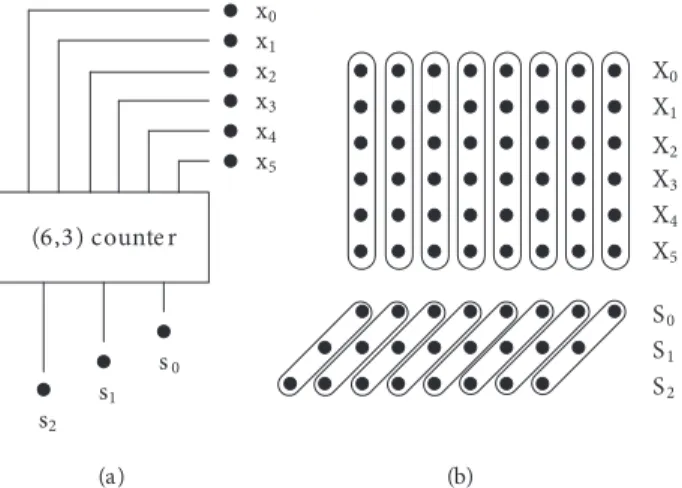
Counter circuits are generally used to reduce the number of operands in a multioperand addition operation, such as reduction of partial products in multiplication. A counter circuit basically counts nonzero input operands and converts the result into radix-2 format [18,19]. For example, a (6,3) counter produces results (000)2 and
(110)2 for the 6-input binary inputs 000000 and 111111, respectively [8,11].
For a (6,3) counter, the result is represented by 3 bits, as the name (6,3) implies, such that 6 inputs are reduced to 3. The representation of a (6,3) counter is depicted in Figure 1a. The multiple operand addition scheme is shown in Figure 1b, where six 8-bit binary numbers X0 ... X5 are reduced to S0, S1, S2. The
conventional binary result is obtained by adding up the 3 outputs S0, S1, and S2 by shifting each output
relatively to their bit weights, as seen in Figure 1b. (6,3) counters are especially useful for 6-input LUT-based FPGAs, where the operation can be handled in a single LUT stage. A (6,3) counter for a single vertical slice can be implemented by three 6-input LUTs, since the function has 3 outputs.
In carry-save arithmetic, each number is represented by a combination of 2 numbers, Z = ( S , C) [6]. In this work, double carry-save architecture is employed as follows:
Za= S0 (1a)
Zb= S1<< 1 (1b)
Zc= S2<< 2 (1c)
(6,3) counte r x5 x4 x3 x2 x1 x0 s0 s1 s2 X0 X1 X2 X3 X4 X5 S0 S1 S2 (a) (b)
Figure 1. (6,3) counter: (a) single bit structure; (b) addition of multiple operands using counters.
The operator “ << k ” represents a k -bit left shift. As shown in Figure 1, each output is relatively shifted by one bit. The redundant number Z represents the addition of 6 binary numbers. The redundant number Z is always a composition of 3 binary numbers ( Za, Zb, Zc) , and whenever a normal binary (i.e. conventional 2’s
complement binary representation) is required, a three-operand addition is accomplished, such that S = Za +
Zb+ Zc .
To summarize, in double carry-save representation, each number is a composition of 3 radix-2 numbers. The digit set of each redundant number Zi is in the set of {0, 1, 2, 3} , where each digit can take values
between 0 ( zia+ zib+ zic = 0) and 3 ( zia+ zbi + zci = 3). Here, each digit of Zi is represented by 3 bits, i.e. zi
= ( zia, zbi, zic) . In this structure, each summation digit is also represented by 3 bits.
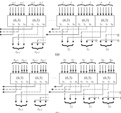
The redundant addition of 2 double carry-save numbers can be accomplished by a single (6,3) counter array. The proposed redundant addition and subtraction operations of X and Y with the result of Z are depicted in Figures 2a and 2b, respectively. Here, each digit of X , Y , and Z is represented as xi, yi, zi,
respectively.
Double carry-save addition operation can be written as:
Z = X⊕Y (2)
Double carry-save subtraction of X− Y can be written as:
Z = X⊕Y + 3 (3)
Here, ⊕ represents (6,3) reduction, and Y represents inverting each of the bits of the redundant number Y . Finally, constant 3 is added to the number, since Y is a composition of 3 normal binary numbers. As an analogy to 2’s complement, where – A is represented as A + 1 , here, constant 3 is added up since each digit is a composition of 3 bits in proposed redundant representation. Since each number is represented by a set of 3 numbers, the double carry representation is defined as −Y = Y +3. Figure 2b shows the redundant subtraction.
zn-2 zn-1 (6,3)
}
}
n-1 n-1 (6,3)}
}
0 0}
z0 (6,3)}
}
1 1}
(6,3)}
}
n-2 n-2 (6,3)}
}
2 2}
z1 0 0 0 z2}
}
s0 s1 s2 s2 s1 s0 s2 s1 s0 s2 s1 s0 s2 s1 s0 (a) xn-1 yn-1}
}
(6,3) xn-2 yn-2}
}
(6,3) x2 y2}
}
(6,3) x0 y0}
}
(6,3) x1 y1}
}
(6,3) zn-2 zn-1}
z0}
}
z1 1 0 1 z2}
}
s0 s1 s2 s2 s1 s0 s2 s1 s0 s2 s1 s0 s2 s1 s0 (b)Figure 2. Redundant double carry-save arithmetic operations: (a) addition; (b) subtraction.
To summarize, the output of (6,3) counter with 6 normal binary numbers at the input results in a single double carry-save format output, as shown in Figure 1b. Two double carry-save format numbers can be added up using a single stage (6,3) counter circuit, as shown in Figure 2a.
It should also be noted that the addition of 3 normal binary numbers (i.e. conventional 2’s complement binary number) to the output of double carry-save output is so trivial that all 3 are written down together, without any operation at all. For example, if 3 numbers X0, X1, and X2 are to be added, Za = X0, Zb =
X1, Zc = X2, then the output is Z = (Za, Zb, Zc) . If 2 numbers are to be added, i.e. X0 and X1, then Za
= X0, Zb = X1, Zc = 0, then the result is again Z = (Za, Zb, Zc) , as in Eq. (1d).
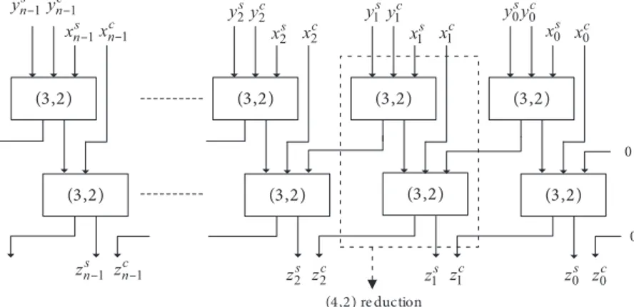
For comparison, the proposed double carry-save, conventional redundant carry-save, and normal binary (i.e. conventional 2’s complement binary) additions are implemented using 6-input LUT devices. The redundant carry-save representation is also named as CS2 [5,20] representation in the literature, since each digit is represented by 2 bits. The redundant carry-save addition operation is represented in Figure 3. The (3,2) blocks represent counters for reducing 3 operands to 2, which have the equivalent function of full adders. Two stages of (3,2) counters implement the function of (4,2) reduction. Here, numbers Y and X are added giving the result Z, where each of X, Y, and Z is represented by a combination of (XS, XC) , (YS, YC) , and (ZS, ZC) , respectively. Here, addition operation is actually a (4,2) reduction, where 4 operands are reduced to 2.
The comparison of the 3 different addition schemes is depicted in Figure 4. As can be seen, carry-propagate addition delay increases with adder size. Normally, the delay is directly proportional to the adder size in the propagate addition. There is a slight nonlinearity after the synthesis. The conventional carry-save operation and proposed double carry-carry-save representation delays are independent from the digit lengths. However, the conventional redundant carry-save operation requires 2 LUT delays, whereas the proposed double carry-save operation requires only a single LUT delay. The area requirement of normal carry-save and double carry-save is the same. Both implementations have approximately twice the area of a carry-propagate adder.
It should also be noted here that, for short adder sizes, carry-propagate addition operation is quite fast due to the fast carry logic blocks of the FPGA fabric. However, the double carry-save method is still much faster than both implementations for any adder size. The timing analyses of the adders are measured using the TimeQuest Timing Analyzer of the Altera QuartusII platform for StratixII FPGAs.
(3,2) (3,2) (3,2) (3,2) 0 (3,2) (3,2) (4,2) re duction (3,2) (3,2) 0 c x0 s x0 s y0y0c c x1 s x1 s y1y1c c x2 s x2 s y2yc2 c n x–1 s n x–1 s n y–1 c n y–1 c n z–1 s n z–1 zc 2 s z2 c z1 s z1 zc0 s z0
Figure 3. Conventional redundant carry-save addition.
0 10 20 30 40 50 60 70 80 90 100 8 16 24 32 Area (LUT)
Adder size (digits) Carry-propagate Double carry-save Carry-save 0 0.5 1 1.5 2 2.5 3 8 16 24 32 Delay (ns)
Adder size (digits) Carry-propagate
Double carry-save Carry-save
Figure 4. Different adder implementations on a 6-input LUT FPGA.
3. Implementation
In this section, a useful example for the double carry-save arithmetic will be given. As mentioned in the previous section, the proposed arithmetic operation is especially useful for recursive multiply-accumulate operations. One of the most commonly used applications for this type of implementation is digital filters. These filters require many cascades of multiply-add operations, and the proposed double carry-save structure is extremely useful for reaching high performance targets. For this reason, a fixed coefficient-based FIR filter will be designed based on a fixed coefficient multiply and add unit.
3.1. FIR filter generation
FIR filters are used for shaping the input signal with the desired frequency response. Discrete time domain representation for an N -tap FIR filter is given as:
y [n] =
N∑−1
k=0
h [k] x [n− k] (4)
Here, x , y , h are the input, output, and transfer function of the filter, respectively. The frequency response H(ω) of a linear-phase FIR filter with impulse response h [ n ] and length N is:
H(ω) =
N∑−1
n=0
h [n] e−jωn (5)
Here, the requirement for a linear filter is that filter coefficients be symmetric or antisymmetric. As a result, the filter coefficients can also be written in terms of amplitude A(ω) and phase terms, as:
H(ω) = A(ω)e−jω(M−1) (6)
For a symmetric filter, M is approximately half the length of the filter tap count. Here, M is given as:
M = ⌊ N 2 ⌋ + 1 (7)
Amplitude A (ω) is a real function of frequency given by:
A(ω) =
M∑−1
m=0
h [m]Tm(ω) (8)
Here, Tm(ω) is a trigonometric function determined by the length and type of symmetry of the filter. The
values of Tm(ω) for the 4 possible types of linear phase FIR filters are given in Table 1 [21]. Table 1. Tm(ω) for different types of linear-phase FIR filters.
Type N Symmetry Tm(ω) 1 Odd Symmetric { 1 2 cos ((M− m − 1) ω) m = M− 1 otherwise 2 Even Symmetric 2 cos ((M− m − 0.5) ω)
3 Odd Antisymmetric 2 sin ((M− m − 1) ω) 4 Even Antisymmetric 2 sin ((M− m − 0.5) ω)
The transposed FIR filter minimizes the critical path of the FIR operation to a single multiply-add operation, as seen in Figure 5a. The linear phase implementation of an odd length filter, realized by symmetric or antisymmetric coefficients, can be realized as seen in Figure 5b.
3.2. Realization of multiply-add operation
Here, the proposed arithmetic will be implemented by generating a multiply-add unit. If the filter specifications are defined, corresponding filter coefficients and number of taps for the filter can be generated using any FIR filter generation algorithm [21]. Since the filter characteristics are predefined, fixed multiplication coefficients are used to generate fixed multiplication blocks.
x D h[N-1] h[N-2] h[0] y D D h[N-3] D D D D D D h(0) y x N h( 2 ) h( +1) h(1) h(2) D D N 2
Figure 5. FIR filter implementation: (a) transposed form; (b) sharing the coefficients.
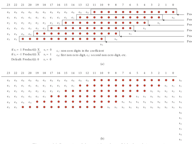
After the filter coefficients are calculated, the multiply and accumulate operations can be implemented according to the redundant arithmetic, as defined in Section 2. The fixed coefficient multiplication for the generated filter coefficients is realized by properly tiling the variables. A multiplication scheme for a 12-bit fixed coefficient and 12-bit data input word length is depicted in Figure 6a. In the example, the coefficient is given as ( 010101010101) . Here, we rename each nonzero digit in the coefficient as ci, where c0=−1, c1 = 1 ,
c2=−1, c3= 1 , c4= 1 , and c5=−1 in the example (enumeration c0...c5is based on the nonzero digit from
the right to the left of the example coefficient). At most, 6 nonzero digits are allowed in any of the coefficients, which is always the general case for 12-bit CSD coded coefficients. A 12-bit CSD coded number has at most 6 nonzero digits, since the number of nonzero digits in CSD format is at most half of the word length [12]. In this representation, higher input data word-length is allowed without increasing the critical path delay. The si in
each line, shown in Figure 6a, also represents the sign bit of any nonzero bit for the corresponding coefficient. The diagram in Figure 6a is an example and not a generalized case. In the generalized case, the shift operations of the coefficients can be arbitrary amounts, depending on the positions of the nonzero digits. Arithmetic right shift operation is applied to the partial product ( n – i) times, where n is the coefficient word length and i is the position of the nonzero digit in the coefficient. Here, ei is the most significant bit (MSB)
of input variable X , if the corresponding coefficient digit is 1. On the other hand, ei is the complement of the
MSB of input variable X if the corresponding coefficient digit is –1. In other words, ei= xM SB⊕ si [19,22].
Here, si is the sign of the incident nonzero coefficient digit. As can be seen in Figure 6a, the sign bit of the
most significant digit of the coefficient ( s5) increases the number of partial products by one, i.e. 7 products
exist in the worst case, and the partial products cannot be fed into a single stage (6,3) counter. The problem is solved using backward sign extension. The (6,3) reduction is performed after this operation. Figure 6b shows the application of backward sign extension.
The multiplication operation for a fixed coefficient with input data is realized by reduction of the partial products, generated as shown in Figure 6b. For the redundant double carry-save representation, each number is a composition of 3 normal binary numbers. As a result, the 6 partial products need to be reduced to 3, in order to make the number compatible with double carry representation. For 6 partial products generated, multiplication with redundant outputs is shown in Figure 7a. In the figure, it can be seen that the multiplication phase consists of a single stage ( n + 1) digit (6,3) reduction scheme. Here, n is equal to the length of the coefficient and the length of the variable, i.e. n = (coef word length + data word length), which is 24 for the given example. The + 1 in the ( n + 1) definition is for the residue reduction, as shown in Figures 6b and 7a. Still, after the reduction, there are residue bits existing together with the multiplier result. The end result is obtained at the
1 15 14 13 12 11 10 9 8 7 6 5 4 3 2 0 P roduct(0) 23 22 21 20 19 18 17 16 s0 s1 s2 s3 s4 s5 1 15 14 13 12 11 10 9 8 7 6 5 4 3 2 0 23 22 21 20 19 18 17 16 s1 s0 s1 s1 s2 s3 s2 s2 s2 s2 s3 s3 s3 s3 s3 s3 s4 s5 s1 s0 s3 s2 s4 s4 s4 s4 s4 s4 s4 s4 s5 s4 s5 s5 s5 s5 s5 s5 s5 s5 s5 s5 e0 e0 e0 e0 e0 e0 e0 e0 e0 e0 e0 e0 e1 e1 e1 e1 e1 e1 e1 e1 e1 e2 e2 e2 e2 e2 e2 e3 e3 e3 e3 e3 e3 e4 e4 e4 e1 e2 e2 e4 e5 e5 P roduct(1) P roduct(2) P roduct(3) P roduct(4) P roduct(5) e0 e0 e0 e0 e0 e0 e0 e0 e0 e0 e0 e0 e1 e1 e1 e1 e1 e1 e1 e1 e1 e2 e2 e2 e2 e2 e2 e3 e3 e3 e3 e3 e3 e4 e4 e4 e1 e2 e2 e4 e5 e5 if ci = 1 P roduct(i): X si = 0 if ci = -1 P roduct(i): X si = 1 De fa ult: P roduct(i): 0 si = 0
ci : non-ze ro digits in the coe fficie nt
c0: firs t non-ze ro digit, c1: s e cond non-ze ro digit, e tc.
(a )
(b)
Figure 6. (a) Generation of the partial products; (b) backward-sign extension.
accumulation step. The accumulation step is also an ( n + 1) digit (6,3) reduction scheme. The other input for the accumulation step comes from the previous tap of the designed filter. The whole multiply-accumulate operation is accomplished in 2 stages of ( n + 1) digit (6,3) counter arrays. At the multiply-add operation output, the result appears in double carry-save format, which is composed of 3 binary numbers.
When 3 or less nonzero digits exist in the coefficients, the multiply phase becomes even simpler, as (6,3) reduction for the multiply phase is removed. The multiplication phase for the multiply-add operation only consists of arithmetic shifts and sign bit padding operations, which are shown in Figure 7b. In this case, the hardware cost for the multiply-accumulate phase is halved, which greatly reduces the hardware cost for the construction of the related filter tap. As a result, the reduction of nonzero digits in coefficients plays an important role in the filter design procedure.
3.3. Filter realization
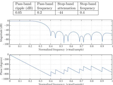
For the performance measurement, a low-pass filter is implemented using the proposed multiply-accumulate unit. The frequency response characteristics of the filter are given in Table 2. The pass-band and stop-band frequencies are normalized to the sampling frequency in the example. The magnitude and phase response plots of the filter are shown in Figure 8.
Given the specifications in Table 2, the filter can be synthesized using any mathematical tool, such as MATLAB, or other kinds of filter design software. However, if the multiplication is to be done in a single stage,
(6,3) R e duction 1 15 14 13 12 11 10 9 8 7 6 5 4 3 2 0 23 22 21 20 19 18 17 16 1 15 14 13 12 11 10 9 8 7 6 5 4 3 2 0 23 22 21 20 19 18 17 16 s3 s3 s4 s4 s5 s5 (6,3) R e duction Multiply-Accumula te R e s ult s1 s0 s0 s1 s1 s1 s2 s2 s2 s2 s3 s3 s3 s3 s3 s3 s2 s2 s3 s3 s4 s4 s4 s4 s4 s4 s4 s4 s4 s4 s5 s5 s5 s5 s5 s5 s5 s5 s5 s5 s5 s5 e0 e0 e0 e0 e0 e0 e0 e0 e0 e0 e0 e0 e1 e1 e1 e1 e1 e1 e1 e1 e1 e2 e2 e2 e2 e2 e2 e3 e3 e3 e3 e3 e3 e4 e4 e4 e1 e2 e2 e4 e5 e5 Multiply P ha s e Accumula te P ha s e Adde r input from pre vious
s ta ge R e s idue 1 15 14 13 12 11 10 9 8 7 6 5 4 3 2 0 23 22 21 20 19 18 17 16 1 15 14 13 12 11 10 9 8 7 6 5 4 3 2 0 23 22 21 20 19 18 17 16 s0 s0 s1 s1 s2 s2 (6,3) R e duction Multiply-Accumula te R e s ult s1 s0 s1 s1 s2 s0 s2 s2 s2 s2 s1 s2 e0 e0 e0 e0 e0 e0 e0 e0 e0 e0 e0 e0 e1 e1 e1 e1 e1 e1 e1 e1 e1 e2 e2 e2 e2 e2 e2 e1 e2 e2 Multiply P ha s e Accumula te P ha s e Adde r input from pre vious
s ta ge
R e s idue
Table 2. Frequency response characteristics of the example filter.
Pass-band Pass-band Stop-band Stop-band ripple (dB) frequency attenuation frequency
0.05 0.2 –44 0.4 0 0.1 0.2 0.3 0.4 0.5 0.6 0.7 0.8 0.9 1 −1000 −800 −600 −400 −200 0
Normalized frequency (×π rad/sample)
Ph ase (de gre es) 0 0.1 0.2 0.3 0.4 0.5 0.6 0.7 0.8 0.9 1 −100 −80 −60 −40 −20 0
Normalized frequency (×π rad/sample)
Magnitude (dB)
Figure 8. Frequency response of the sample filter.
the coefficients must be digitized to 12-bit word length. The word length of the example filter is optimized using the algorithm in [10]. The example filter could be synthesized with 25 taps and 12 digit coefficients. The synthesized coefficients for the filter are given in Table 3. In the table, the coefficients that have 3 or less nonzero digits are marked with asterisks. The coefficients with 3 or less nonzero digits save space in synthesis and increase performance.
Table 3. Optimized coefficients of the filter.
Coefficients of filter F1 with N = 25,B= 12
h(0) = –2−8 (*) h(7) = –2−4 + 2−6 – 2−8 + 2−10 h(1) = –2−7 + 2−9 (*) h(8) = –2−5 – 2−7 – 2−10 (*) h(1) = –2−11 (*) h(9) = 2−5 – 2−9 (*) h(3) = 2−6 – 2−8 – 2−11 (*) h(10) = 2−3 + 2−6 + 2−8 (*) h(4) = 2−6 + 2−8 (*) h(11) = 2−2 + 2−8 + 2−10 (*) h(5) = 2−7 + 2−10 (*) h(12) = 2−2 + 2−4 – 2−6 + 2−8 h(6) = –2−6 – 2−8 – 2−10 (*) h(n) = h(24-n) for n = 13, 14, . . . , 24
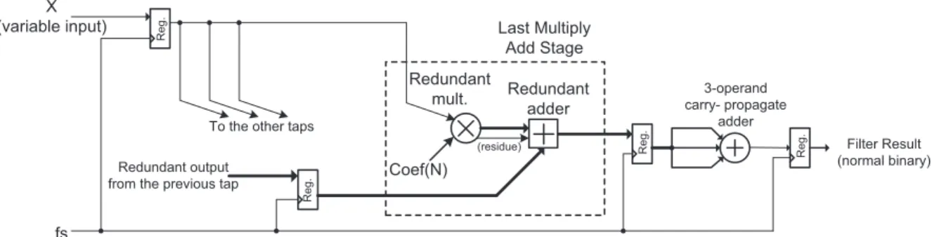
The last stage of the redundant multiply-add operation is pipelined with registers, and between the pipelines, a three-operand addition is handled to convert double carry-save representation to normal 2’s com-plement binary output in the end. The representation of the multiply-accumulate operation is shown in Figure 9. The representation only shows the last multiply-add operation of Figure 5b. As the figure reveals, the re-dundant output of the system is converted to normal binary by insertion of a three-operand adder circuit after the last tap of the multiply-add operation.
Redundant adder fs Last Multiply Add Stage Filter Result (normal binary) 3-operand carry- propagate adder Coef(N) R e g . Redundant output from the previous tap X
(variable input)
Redundant mult. To the other taps
(residue) Reg . R e g . R e g .
Figure 9. Representation of multiply-add operation and conversion to normal binary.
coefficient multipliers and carry-propagate adders in normal binary mode, using a total 6-input FPGA fabric. In the second implementation, firm multipliers are used, which are generally recommended for DSP operations in FPGA fabrics. For the accumulation phase, carry-propagate adders are used in the second implementation. In the third implementation, proposed double carry-save implementation is handled for multiply and accumulate units. In each of the implementations, the architecture in Figure 5b is used.
Fixed coefficient multipliers are designed using the Altera QuartusII Megafunctions Wizard. Each of the implementations is synthesized using Altera Quartus II software. The comparison of hardware cost and maximum operating speed is given in Table 4. A fast redundant signed-digit-based FIR filter [17] is also added for comparison. The implementation in [17] also has a redundant representation with carry-free arithmetic utilizing 8-bit coefficients with 8-bit data word-length and 16 taps, where the recorded speed is 293 MHz in a 6-input LUT-based FPGA. Our implementation performance is far beyond the referenced implementation; in addition, our implementation has larger coefficient and data widths (both of which are 12 bits wide) with 25 taps. The hardware resources used are not reported in the implementation [17]. The speed performance comparison of the filter implementations is shown in Figure 10. The synthesized filter is functionally tested on the Altera Stratix II DSP Development Kit by filtering out the high performance component of a mixture of 2 sinusoidal signals.
Table 4. Comparison of various implementations of the filters.
Implementation Hardware cost Maximum speed (MHz)
ALUT + DSP blocks Register count Fixed coefficient soft multiplier 814 ALUT 576 188 Firm multiplier 576 ALUT + 26 DSP blocks 600 190
Proposed method 1515 ALUT 1491 446
0 50 100 150 200 250 300 350 400 450 500
Soft Multiplier Filter Firm Multiplier Filter Signed-Digit Filter [17] Proposed Filter
Speed (MHz)
Filter Implementation Type Figure 10. Filter performance comparison.
Various FIR filter implementations and a detailed analysis of filter design are planned for a future study. However, we found that as the number of taps in the design is increased, the maximum speed of the system is gradually reduced. The reason is the loading effect of the input signal. Since the input signal is connected to every tap in the transposed FIR filter structure, as the number of taps increase, the capacitive loading of the interconnections dominates. This effect also occurs in conventional soft multipliers.
It should be mentioned that the FIR filter is simply a good example of implementation. Together with fixed coefficient architectures, variable coefficient multiply-add units and other arithmetic structures that require multiply-add operations can be tailored according to the requirements. The arithmetic operations proposed here can be applied to high performance systems, which recursively require addition, and multiplication operations such as digital filtering, matrix multiplication, and other similar structures.
4. Conclusion
In this work, double carry-save arithmetic is presented for carry-propagation-free operations. Using the proposed scheme, the critical path for each multiply-add operation is reduced to only 2 LUT cascades, one for the multiply operation and the other for the accumulate operation. The hardware is generated using only (6,3) counters, giving a very regular structure.
For testing the performance, a fixed coefficient FIR filter implementation methodology, suitable for 6-input LUT-based FPGAs, is presented. The proposed implementation resulted in more than 100% speed improvement over conventional fixed coefficient multiplication-based FIR filtering schemes. The filter frequency is recorded as 440 MHz, whereas any arithmetic circuit, such as a simple AND gate delay, is limited to 500 MHz for the StratixII FPGAs. By exploiting the compatibility of the number system with the FPGA hardware, an extreme speed advantage is gained. To our knowledge, the implementation presented here provides the fastest speed in 6-input LUT-based FPGAs for multiply-add operations.
References
[1] Xilinx Inc. Xilinx Virtex-5 Family Overview. San Jose, CA, USA: Xilinx, 2009.
[2] Altera Corporation. Altera Stratix II Device Handbook. San Jose, CA, USA: Altera Corporation, 2009.
[3] Parhami B. Generalized signed-digit number systems: a unifying framework for redundant number representations. IEEE T Comput 1990; 39: 89–98.
[4] Ercegovac M, Lang T. Digital Arithmetic. San Francisco, CA, USA: Morgan Kauffman, 2004.
[5] Phatak DS, Goff T, Koren I. Constant-time addition and simultaneous format conversion based on redundant binary representations. IEEE T Comput 2001; 50: 1267–1278.
[6] Noll TG. Carry-save architectures for high-speed digital signal processing. J VLSI Signal Proc 1991; 3: 121–140. [7] Altera Corporation. Advanced Synthesis Cookbook: A Design Guide for Stratix II, Stratix III, and Stratix IV
Devices. San Jose, CA, USA: Altera Corporation, 2009.
[8] Samueli H. An improved search algorithm for the design of multiplierless FIR filters with powers-of-two coefficients. IEEE T Circuits Syst 1989; 39: 1655–1668.
[9] Yurdakul, A, D¨undar G. Fast and efficient algorithm for the multiplierless realisation of linear DSP transforms. IEE PCirc Dev Syst 2008; 149: 205–211.
[10] Aktan M, Yurdakul, A, D¨undar G. An algorithm for the design of low-power hardware efficient FIR filters. IEEE T Circuits Syst 2008; 55: 1536–1545.
[11] Hartley R. Subexpression sharing in filters using canonic signed digit multipliers. IEEE Trans CircuitsII 1996; 43: 677–688.
[12] Parhi K. VLSI Digital Signal Processing Systems: Design and Implementation. 1st ed. New York, NY, USA: Wiley, 1999.
[13] Ortiz M, Quiles F, Hormigo J, Jaime FJ, Villalba J, Zapata EL. Efficient implementations of carry-save adders in FPGAs. In: IEEE International Conference on Application-Specific Systems, Architectures and Processors; 7–9 July 2009; Boston, MA, USA. New York, NY, USA: IEEE. pp. 207–210.
[14] Kamp W, BainbridgeSmith A. Multiply accumulate unit optimised for fast dot-product evaluation. In: ICFPT 2007 International Conference on Field-Programmable Technology; 12–14 December 2007; Kitakyushu, Japan. New York, NY, USA: IEEE. pp. 349–352.
[15] Parandeh-Afshar H, Brisk HP, Ienne P. Improving synthesis of compressor trees on FPGAs via integer linear programming. In: DATE 2008 Design, Automation, and Test in Europe Conference; 10–14 March 2008; Munich, Germany. New York, NY, USA: IEEE. pp. 1256–1261.
[16] Kamp W, Bainbridge-Smith A, Hayes M. Efficient implementation of fast redundant number adders for long word-lengths in FPGAs. In: FPT 2009 International Conference on Field-Programmable Technology; 9–11 December 2009; Sydney, Australia. New York, NY, USA: IEEE. pp. 239–246.
[17] Cardarilli GC, Pontarelli S, Re M, Salsano A. On the use of signed digit arithmetic for the new 6-inputs LUT based FPGAs. In: IEEE International Conference on Electronics, Circuits, and Systems; 31 August–3 September 2008; St Julian’s, Malta. New York, NY, USA: IEEE. pp. 602–605.
[18] Koren I. Computer Arithmetic Algorithms. Natick, MA, USA: AK Peters, 2002.
[19] Parhami, B. Computer Arithmetic: Algorithms and Hardware Designs. 2nd ed. Oxford, UK: Oxford University Press, 2008.
[20] Gonz´alez AF, Mazumder P. Redundant arithmetic, algorithms and implementations. Integration 2000; 30: 13–53. [21] Mitra S. Digital Signal Processing: a Computer-Based Approach. 2nd ed. New York, NY, USA: McGraw-Hill, 2001. [22] Weste N, Harris D. CMOS VLSI Design: A Circuits and Systems Perspective. 4th ed. Boston, MA, USA: