H. MEHREZ AND S. CIRACI
Department of Physics,
Bilkent University,
06533, Ankara, Turkey
Abstract. This paper presents a detailed analysis of conductance and
atomic structure in metal nanowires under tensile stress. We calculate the
variation of conductance with the crossection of the constriction between
two reservoirs, that is represented by three-dimensional circularly symmet
ric potentials. The absence of several observed features in the calculated
conductance variations, in particular sudden jumps, suggests that the dis
continuous rearrangements of atoms under stretch dominate the electron
transport. To analyze the variations of atomic structure, we performed
simulations based on the state of the art molecular dynamics simulations
and revealed novel structural transformations. It is found that yielding and
fracture mechanisms depend on the geometry, size, atomic arrangement
and temperature. The elongation under uniaxial stress is realized by con
secutive quasi elastic and yielding stages; the neck develops mainly by the
implementation of a layer with a smaller crossection at certain stages of
elongation. This causes to an abrupt decrease of the tensile force. Owing to
the excessive strain at the neck, the original structure and atomic registry
are modified; atoms show tendency to rearrange in closed-packed struc
tures. In certain circumstances, a bundle of atomic chains or single atomic
chain forms as a result of transition from the hallow site to the top site
registry shortly before the break. The origin of the observed "giant" yield
strength is explained by using results of present simulations and
ab initio
calculations of total energy and Young's modulus for an infinite atomic
chain.
213
G. Abstreiter et al. (eds.), Optical Spectroscopy of Low Dimensional Semiconductors, 213-234.
214
1. Introduction
The optical, electronic and mechanical properties of condensed systems with nanometer dimensions can be rather different from those of the bulk. The effects of reduced size and dimensionality, in particular properties lead ing to novel devices have been subject matter of several research works in the last decade[l]. By pulling the tip of a scanning tunneling micro scope (STM) after the nanoindentation[2-6] or by bending a mechanically controllable break junction[7], long metal wires with diameters in the range of few Ap have been produced. As the crossection of the wire is reduced by stretching it continuously, the two terminal conductance
G
is measured. The measured conductance showed irregular and sudden changes with stretchs;
the detailed behavior of which was not only sample specific, but also was varying in different scans of the same experiment. The abrupt falls ofG( s)
became generally sharper and closer to the integer multiples of quantum conductance
(G
O=
2e2 /h
per two spin) with decreasing crossection prior to the break of the neck. This has been taken as a manifestation of the quantization of conductance in atomic size wires ( or connective necks). In contrast to various quantization arguments[5,6], some authors related abrupt variation ofG(
s)
to the irregular and discontinuous changes of the crossection of the wireA(
s)
in the course of stretch[8-11]. Presently, these predictions were strengthened by the experimental results[12,13] that have been obtained by using a combination of STM and AFM ( atomic force microscope). These experiments have shown that any sudden change in conductance is accompanied by an abrupt modification of atomic structure and hence the crossection of the neck. The yield strength uy measured shortly before the break has been found much higher than that of the bulk. The narrowest diameter of the nanowire prior to tlie break is only a few angstrom; it has the length scale Ap, where discontinuous ( discrete) nature of the metal dominates over its continuum description. For exam ple, in this length scale, the level spacings of electrons (0.1 -leV)
become easily resolved even at room temperature, and any change of atomic struc ture may lead to detectable changes in the related properties. For example the ballistic electron transport through nanowire is expected to be closely related with the atomic structure at the narrowest part of the connective neck. It becomes now clear that the mechanical properties, in particular the yielding mechanisms of the nanowires are quite different from those of bulk material.We believe that the subject of dispute about the quantization of conduc tance emerges from the diverse criteria; this will be clarified in the present work by the analysis of ballistic transport in a nanoindentation and in an atomic size connective neck that is pulled between two electrodes. In this
paper, we investigate the ballistic electron transport on the idealized wires which have circularly symmetric potential but short necks as in the exper iment. Since the calculated variation of
G
with the radius does not exhibit sharp step structure, we seek the origin of the abrupt jumps in the struc tural changes of the wire during stretch. To this end, we carry out state of the art Molecular Dynamics (MD) studies which indicate a clear con nection between the strain induced atomic rearrangement and conductance variations. We found novel atomic processes and atomic rearrangements induced by the applied stress. By using these results we provide a consis tent interpretation for various structures ofG
observed in the course of stretch. W hile the step falls ( or jumps) of G(s)
are associated with the sud den changes in the crossection, the spikes on the plateaus may be due to transient motion (migration) of atoms in the narrowest region of the neck or resonant tunneling through the constriction. The positive slope observed on the last plateau of Pt and Al wires[7] is due to increasing local density of states p(r, EF) at the neck which undergoes a structural transformation under extreme strain.2. Conductance in the Nanowire
How the conductance of a mesoscopic object depends on its size and di mensionality has always been attractive, as well as intriguing subject for researchers. As early as 1957, Landauer[14] proposed that the conduction in a solid is a scattering event, and that transport is the consequence of the incident current flux. Based on the counting arguments of the transmission
T,
and reflectionR,
he derived his famous formula for the conductanceG
=
(2e2 /h )(T
/
R).
Almost three decades ago Sharvin[15] pointed out theresistance of a ballistic channel ( or point contact) and developed a for malism in the semiclassical regime. Nowadays, almost defect-free electronic devices have been fabricated, which have dimensions, in one or more di rections, on the quantum scale. The two terminal conductance of such a quasi ID device ( or constriction) fabricated from the high mobility GaAs Ah-x GaxAs heterojunction[16,17] (which have width w in the range of
Fermi wavelength >.F, and length d smaller than the electron mean free
path) were found to change with w approximately in steps of 2e2 /
h.
Thisobservation has been interpreted as the quantization of the ballistic conduc tance. It became clear from subsequent studies[9,18,19] that the motion of electrons in the constriction is transversally quantized if d "' >.F, and then
its level spacings become in the range of a few Kelvin, if w is in the range of >.F. A n-fold degenerate current-carrying state becomes conducting and
hence G increases by 2e2n/ h whenever its energy coincides with EF; this
216
with
w
displays sharp steps of integer multiples of 2e2 /h,
and flat plateausform between two consecutive steps provided that the potential in the con striction is uniform, temperature and bias voltage are low, and tunneling contribution is negligible. Otherwise, conduction channels mix significantly, the opening of channels are delayed, sharp step structure is smeared out and step heights are lowered[9].
The atomic size point contact was produced first by the STM: By displac ing the tip towards the sample surface, the conductance were measured in a wide range covering tunneling and ballistic regimes. The experimental
logG
versus tip displacement either exhibits a linear variation and then saturation at the first plateau before a jump, or it ends the linear variation directly by a jump[2].Theoretical studies[8,20,21] showed that the two terminal conductance at the single atom contact shall be in the range of 2e2 /
h.
Furthermore, it hasbeen shown that the observed jumps of conductance originate from the dis continuous and abrupt change of crossection of the contact[8-10].
Better controls of dimensions[4-6] has led to a renewed interest in the trans port through the connective necks produced by STM. The principle issue is to what extent the observed structures in the conductance versus stretch curve
G(
s
), comply with the quantization of ballistic conductance. It is expected that the atomic structure of the neck is rather irregular and the potential is non uniform. The narrowest part of the neck, which determines conductance, is rather short. In those circumstances, the sharp quantization with marginal channel mixing should not occur. Of course the transversal motion of electrons in the neck is quantized with significant level spacing; the effect of this quantization is reflected to the transport. We strengthen our arguments by performing calculations of conductance for uniform con strictions, where the channel mixing shall be insignificant. We will show that the features ofG( s)
orG( A)
for these idealized wires are rather dif ferent from the observed behavior.3. Ballistic Free Electron Model
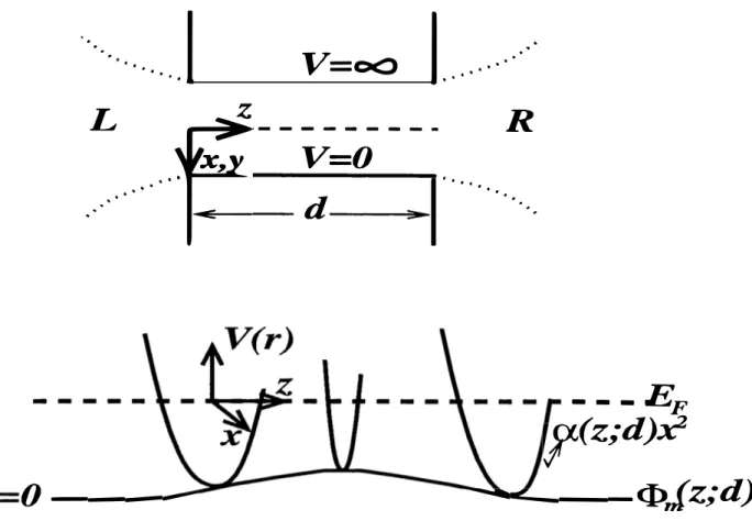
The nanowire which is connected to the left (L) and right (R) reservoirs ( or metal electrodes) by a neck is viewed as a constriction represented by a
3D
confining potentialV(r).
A free electron of the L-reservoir with wave function W i, enters in the constriction with a finite momentum in the z-direction and evolves into current-carrying states[9]. These current carrying states, either propagate to the R-reservoir or are occasionally scat tered, and eventually reach the R-reservoir. The current-carrying states in side the constriction are determined by using multiple boundary matching method, and the conductance is calculated by evaluating the currentoper-·· .. oper-·· ... ,
V=o0 , ... /
L
R
�x.
z __
v,.:-o--·
.. ···
. . .
d
1 · ..
··· ...
---E
F
ry,<z;d)x2
V:
0---
----...""'----<P,J z;
d)
Figure 1. Schematic description of the constriction connected to the left (L) and right (R) reservoirs, which is used to model the electron transport through a nanowire. (a) The infinite wall cylindrical potential with abrupt ( continuous line) and trumpet-like ( dotted line) connections to the reservoirs. (b) Schematic description of the parabolic potential in the (xz)-plane
ator. As a simplest approximation, the infinite wall cylindrical potential is
used for
V(r):
V(r)
V(r)
0 for (x
2+
y
2)11
2<
R(z)
oo otherwise
(1)
Here
R(z)
is the radius of the constriction which depends on the
z
coordi
nate.
Our self-consistent field (SCF) pseudopotential calculations for infinite Al
and Na atomic wires with optimized nearest neighbor distance, suggest that
the parabolic potential form in the transversal direction is better suited for
V(r).
The self-consistent pseudopotential is parameterized as follows:
V(r)
=
�m(z; d)
+
a(z; d)(x
2+
y
2)
(2)
Here d is the length of the constriction ( or neck), and
�mis the sad
dle point potential, which occurs for finite constriction. The two differ
ent approximations for the constriction potential are described in Fig.I.
We note that these potentials with circular symmetry are very idealized de
scription of the realistic potential inside the constriction. Because of circular
218
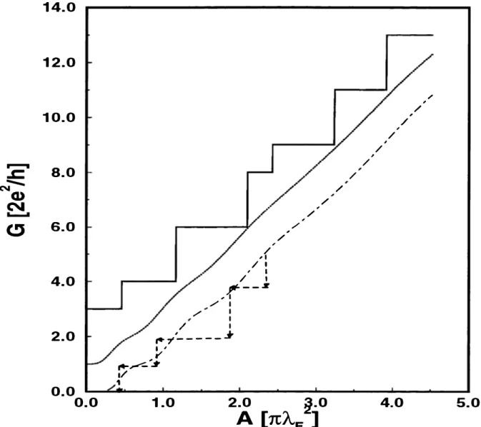
14.0 12.0 10.0::c'"
8.0
N-. G) N CJ 6.0 4.0 2.00.0
0.0
/ /, , I /I • I / I _,r--% / I /:
/ I / /, ,/'..--/---*
I • ,.,
..-.,.r-,
1/ t 1.0 2.0 �-0A [1tA.F
1
/ / / , / ,/ , / ,/ 4.0 /'5.0
Figure 2. Conductance G versus crossection A for a constriction with an infinite wall cylindrical potential and abrupt connections to reservoirs. Continuous line is for the infinite and uniform neck; dotted line is the quantum Sharvin regime with d - 0. Uniform and finite neck having d - )..F corresponds to dash-dotted line. The discontinuous change of
A
during stretch give rise to sharp steps as schematically described by dashed lines. The curves are up-shifted for clarity.symmetry, one can obtain analytical solutions for the wave functions in the
transversal (xy)-plane. For example, in the parabolic confinement given
by Eq.2, the wave functions can be separable in the transversal (xy)-plane
and in the longitudinal z-direction, and the transversal ones become 2D
harmonic oscillator wave functions.
By using the above forms of the potentials with the abrupt or trumpet-like
connections to the reservoirs, we calculate the variation of the conductance
as a function of the crossection. By comparing the calculated curves
G(A)
with the conductance versus stretch curves obtained experimentally, we
aim to draw conclusions on the quantization of ballistic conductance in
nanowires or connective necks. Figure 2 illustrates our results for
G
ver
sus crossection
A
for the infinite wall cylindrical potential with uniform
radius
R
that is connected abruptly to the reservoirs. The dotted curve
corresponds to Sharvin's conductance of a contact with d
rv0. Owing to
d <{::'. >.F, the quantization is not completed and step structure is smeared
out by tunneling. On the other hand, as d
-too, the current carrying states
have the same quantization at every point along the constriction. Tunneling
and mixing of channels do not take place and hence, the variations of G
with A displays sharp step structure. Here, any quantized state that coin
cides with the Fermi level opens a conduction channel and contributes to
the ballistic conductance by 2ne
2 /h; n being the degeneracy of the state. In
an intermediate situation, i.e d
rv>.F, the effect of quantization of transver
sal state in the neck becomes apparent in the
G(A)
curve; but neither the
steps are sharp nor the the plateaus are flat. Calculations by using uni
form parabolic potential with abrupt connections to L- and R-reservoirs
and with d
=
>.F/2 and d
=
>.F, lead to essentially the same conclusions.
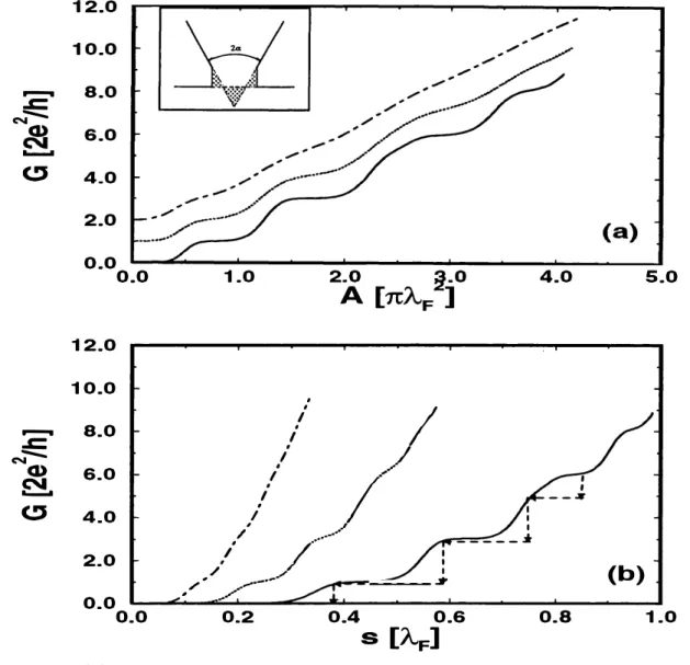
Next we consider a constriction potential which has abrupt connection
from one end and trumpet-like connection from the other end. Such a po
tential may correspond to the nanoindentation of an STM tip into a flat
metal surface. The crossection and the length of the contact can be calcu
lated as a function of the displacement of the tip towards the surface by
using continuum contact mechanics or simply by assuming incompressible
material in the nanoindentation. Figure 3 shows variation of
G
with the
crossection
A
and with the push s for different cone angles 2a. We note that
the contact made by a tip having relatively larger cone angle, has shorter
length d and hence relatively weaker step structure.
Two important approximations are made for the above calculations:
i) Within the continuum approximation, we assumed that the crossection
of the neck varies continuously. This may be a reasonable approximation
for a metal wire which has large diameter (2R � >.F). However, as we show
in the next section, the crossection of an atomic size wire changes discon
tinuously.
ii) The potentials we used in calculating G are too idealized and have cir
cular symmetry. The simulation of stretch in the next section show that
the crossection of the wire is not circular, and its surface is rather rough.
The constrictions we studied above have weak features in the
G(A)
curves that are different from the experimental curves. If the structure of
experimental
G(A)
or
G(s)
is attributed to the quantized conductance the
conditions of the above constrictions would be even more suitable for per
fect quantization. Apparently, the earlier interpretation of the experimental
results have to be revised. In what follows, we show that the discontinuous
rearrangement of atoms and structural transformations are essential for a
better understanding of the observed
G( s)
curves.
220
-.c:
--
G)CJ
-.c:
--
G)�
CJ
12.0 10.0 8.0 6.0 4.0 2.0 0.0 0.0 12.0 10.0 8.0 6.0 4.0 2.0 0.0 1.0 /// / I ' I ' I 4.0 ;" / I ---"/_.,, �
_____ _;.
(b)
5.0 0.0 0.2 0.4 0.6 0.8 1.0S [A.
F]
Figure 3. ( a) G versus A for a contact formed by an STM tip indenting the substrate sur face. (b) same curves plotted as a function of the displacement s of the tip towards sample. Dash-dotted, dotted and continuous curves correspond to the cone angles 2a
=
120°, 90°and 60°, respectively.
4. MD-Simulations
4.1. DESCRIPTION OF MD-SIMULATIONS
In this section, we study yielding and fracture mechanisms of nanowires
that are pulled by an external agent. To understand the origin of these
mechanisms and abrupt force variations[12,13), we perform an extensive
analysis of atomic structure in the course of pulling. In particular, we fol
low the motion of the neck atoms and examine their coordination numbers
and the structure of atomic layers during the abrupt force variations. We
use embedded atom (EA) potential[22-24), and carry out simulations based
on the MD method for the Cu nanowires made from (001) and (111) atomic
planes[25). Recently, the MD simulation is proven to be powerful method to
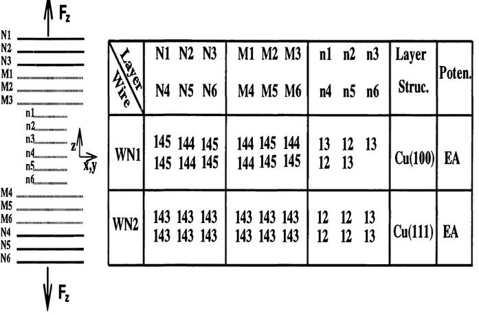
t
F,
Nl � ... ��
N2 ����
N3 ����
Ml""""'''"""""'"'"''''''''"""""'''' M2 """""'"""""'"'"'''''''"""""'''' M3 """"'''"""""'.""''''''"""""'''nl ... , .... ,,,,,,
n2,,,,,,,,,,,.,,,,,,,,,,,
�
n3 ... ,,, ... ,,, Z
n4,,,,,,,,,,,,, ... ..
nS ... ,,,,,, ... ,,,,,,..
,y
n�IIIIIIIIIIIIIHIIIIIIIII M4 """'''""""""'""''""""""""''"' MS""""''""""""""'''''''''"""""''' M6 """""''"""""·""''"'''"""""'''N4 ����
NS ����
N6 ����
� F,
�
Nl N2 N3
�
N4 NS N6
WNl
145 144 145
145 144 145
WN2 143 143 143
143 143 143
Ml M2 M3 nl n2 n3 Layer
Poten.
M4 MS M6 n4 n5 n6 Struc.
144 145 144 13 12 13
144 145 145 12 13
Cu(lOO) EA
143 143 143 12 12 13
143 143 143 12 12 13 Cu(lll} EA
Figure
4.
Schematic description of the Cu nanowires. The layers labeled by N, M and n are described in the text. The number of atoms in each layer and their 2D structure before pulling are indicated. The x- and y-axis lie in the atomic [(001) or (111)] planes. The z axis coincides with the axis of the wire; the tensile force F z is applied along the z-axis. EA stands for the embedded atom potential.reveal the atomic rearrangement under tensile stress[3,5,25- 27]. The wires we studied have two ends that are connected by a neck, and have quasi circular crossections. Their structures are summarized in Fig.4. Last three layers at both ends (N1, N2, N3 and N4, N5, N6) are robust: All the atoms in these layers are translated solidly along the stretch direction only by the in crement
!:ll;
otherwise they are kept fixed during the MD-steps. These fixed three layers are assumed to be connected to the external agent that applies the tensile stress. Atoms in the following three layers adjacent to the fixed ones (M1,M2,M3 and M4,Ms,M6) and those of the neck(nl, n2, n3 ... )
are fully relaxed during the MD-steps. The nanowire indicated byW Nl
is formed from Cu(OOl) atomic layers. The wire itself is represented by a periodically repeating system in the ( xy )-plane. The z-axis is taken to be parallel to the axis of the nanowire.W
N2 is made from Cu(lll) atomic planes, and it is investigated atT
=
300K
andT
=
150K. The pulling (stretch) is realized by displacing the fixed layers (N
's) solidly along the z-direction by the increment of length!:ll
(0.1.A.). After each increment, the atoms of the wires(M's
andn's)
are relaxed to find their new po sitions. Simulations are performed with time steps ofO.lps
Between two222
...
0.0(a)
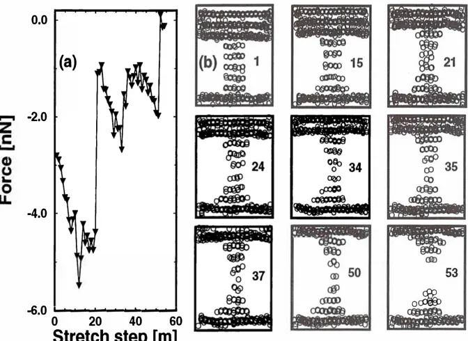
-2.0 -4.0 -6.0 ... _ _.__._... ___ 0 20 40 60Stretch step [m]
53
0�Figure 5. (a) The variation of the force F r(nN) with the strain or elongation along the z-axis applied by pulling the end layers of Cu (WNI) by mt:.l at T
=
300K. (b) The side views of the nanowire showing the atomic positions at some relevant stretch values m.subsequent stretches of b..l the nanowire is relaxed for 2500ps. The tensile
force F z ( which is the attractive force between the fixed top three layers
and the rest of the wire) is obtained after averaging over the last 800fs, so
that the force fluctuations are minimized.
4.2. MD RESULTS FOR Cu(OOl) NANOWIRE
In this section we examine the elongation and various physical events dur
ing the stretch of the nanowire,
W N
1 at
T
=
3001(. The initial atomic
configuration of the nanowire is described in Fig.4. The interlayer distance
between the bulk Cu( 001) layers is c ,.._, 1.8.A ( approximately half of the
lattice parameter, i.e ,.._, a/2). Initially, the layers of the wire have A-B-A-B
sequence; the atoms of the B-layer face the hallow sites (the center of square
unit cell) of the adjacent A-layers. We specify this stacking as the H-site
registry. In Fig.5, we illustrate the variation of F z as a function of stretch
mb..l, ( m, being an integer multiples of increment) and the side views of the
structure at the neck region. The F z( m) curve displays small fluctuations
and also abrupt jumps. The magnitude of the average force increases with
increasing m between two consecutive jumps. This is the "quasi" elastic
stage[l3] .
Our results clearly indicate that a new abrupt jump of F z ( m )
occurs whenever approximately
rv1 8 - 20 increments are made in an elas
tic stage following the previous jump. Stated differently,
the tensile force
makes a sudden jump and decreases significantly
whenever the length
l
of
the nanowire is elongated by approximately interlayer distance, c. The jump
of F z ( m ) starts as the atomic structure of the neck becomes disordered; it
lasts until a new layer with relatively smaller crossection is generated. This
is the
yielding stage.
The formation of neck layers at fairly regular intervals
was predicted earlier[5]. The overall behavior of F z (m) is in agreement with
the experimental results[3, 1 2, 1 3]. We now examine these in detail.
At the last increment before the first jump in F z ( m) (
m
rv1 9 ), the layer
structure in the neck is destroyed, and becomes disordered; however it is
recovered after a few increments, at
m
rv24, with the creation of a new
layer (see Fig. 5 ). At the end of this transformation, the crossection of the
neck is reduced from 8 atoms to 5 atoms; whereas the crossection of neck
layers adjacent to end layers (
nl
and
n5)
is not altered. The local reduction
of the crossection due to stretching causes
IF zl
to reduce, and hence the in
terlayer spacings between
M3
and
nl
( and similar spacing at the other end)
to decrease. The layer structure of the neck is conserved until
m '.:::'. 33. Be
yond that point each increment of stretch by b.. l causes one atom from the
central layer to migrate and stay in the adjacent interlayer spacing which
already became wide open due to pulling from
m = 25 to m =33. This way
a new "layer" with two atoms is formed. As a result, the crossection of the
connective neck is further reduced with three central layers formed by 5,2,3
atoms, respectively. Owing to the repulsive force induced between the new
layer and adjacent ones,
IF zl
decreases abruptly. The asymmetric distribu
tion of atoms in the neck layers may be due to a dynamical effect and due to
stretch of the wire from one end, as well . However, in the steps from m=35
to m = 38, the asymmetry is lifted by a peculiar, transient event which may
be relevant for transport properties: One of the two atoms in the neck layer
created at
m = 35, jumps back to the layer it emerges. During the follow
ing increments, the single atom neck is strengthen by the inclusion of one
atom from another layer so that the necking becomes uniform by the layers
including 4,2,4 atoms. Due to this exchange of atom, the conductance is
expected to get a transient dip provided that its duration is long enough.
In fact, such a dip has been observed[5]. The two-atom neck becomes stable
until the break; but the atoms rotate in the (xy) - plane and they become
slightly inclined in the z-direction . Such a fluctuation in configuration may
give rise to changes in the conductance. It is also seen that the narrowest
crossection of the neck prior to the break can have two atoms.
The above results point to the fact that the structural transformations fol
lowed by the abrupt change of F z result in necking. An additional layer is
224
(a)
(b)
(c)
&• �
+
�
t· �· +
�·� �·
�-�
(w
e-�
�- I� �
0
0
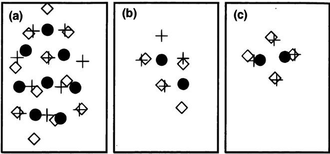
Figure 6. The top view of three layers at the neck showing atomic positions and their
relative registry at three different levels of stretch. (a) Before the first yielding at m
=
1 5for layers n 2 , n 3 and n4, with their atomic positions indicated by + , • and 0 , respectively. (b) corresponds to m
=
38, just after the second yielding, the structure keeps its registry;while ( c) corresponds to m
=
46, starting the formation of bundle structure. The position of atoms in the third, fourth and fifth layers are indicated by +,• and 0, respectively.formed and the narrowest crossection decreases usually by more than one
a.tom. In addition to these abrupt changes, we find another mechanism in
necking that gives rise to relatively smaller and also slower changes in the
crossection. This is a single a.tom process, in which individual a.toms mi
grate from central layer towards the end layers. The tendency to minimize
the surface area and hence to reduce surface energy is the ma.in driving
force for this type of necking.
Next we examine atomic rearrangements and structural changes in ev
ery atomic layer, which become gradually non-planar under tensile stress.
The arrangements of a.toms in the layers a.re shown in Fig.6. In our study
we have found that upto m
=
12, the Cu(OOl) structure in the neck layers
exhibits very small and random deformation ( with atomic displacements
less than 10% and with no preferable direction), especially those a.toms
a.way from the boundary. As shown in Fig.6-(a.), the original stacking and
registry are kept with least deformation. Beyond a certain stretch, the neck
a.toms start to built up a structure which deviates from the A-B-A-B stack
ing sequence of the ideal Cu(OOl) planes.This deformation starts earlier in
the layers n2, n3 and n4 at m
=
15. Here we note its two aspects: First,
the intera.tomic distances have slightly increased, especially those of central
layers. Second, the 2D square lattice changes and then looks like a hexag
onal lattice. U pan further elongation of the na.nowire, the rest of the neck
undergoes the same deformation. The tendency towards a 2D hexagonal
like lattice is mediated by the reduced interlayer interaction as a result of
stretch; the atoms try to take relatively low energy configuration in the
quasi independent layer behavior. As soon as a new neck layer is formed
(at m "' 24), the original features, especially the registry of the Cu(OOl)
layers are recovered at both ends of the neck (nl,n2 and n5,n6 layers).
These layers (being close to the relatively more stable M
3and M
4layers)
are forced to return to the original structure. Whereas it is impossible to
recover original A-B-A-B sequence of the Cu(OOl) planes and to match the
new layer to the adjacent ones, the incommensurability and deviation from
the bulk ordering continues until a new layer is formed. In the present case
a new "layer" made of two atoms at the neck is formed at m "' 33 -35, but
they do not have enough extension to be considered as a real atomic layer.
An interesting situation owing to the reduced interlayer interaction and
excessive tensile strain appears in the last stage of stretch: The H-site reg
istry disappears eventually shortly before the break and hence the atoms of
the adjacent neck layers tend to face the top (T)-sites. This way they are
aligned to form atomic chains as shown in Fig.6 . As a result, the crystal-like
structure and original registry at the neck is replaced by a bundle of atomic
chains. In some circumstances, a single atomic chain can form rather than
the bundle. Earlier, ab initio calculations confirm that the T-site registry
is only a local minimum occurring at relatively larger interlayer separation
for the Al(lll) and Al(OOl) slabs[28] . However, for some materials oriented
in certain atomic planes, the break can take place before such a transition.
The transition from the H-site registry to the T-site registry leading to
a bundle of chain structure is interesting not only for the point of view of
structural modification, but also for novel properties[27,30] (such as "giant"
yield strength[12,13] and positive slope of conductance variations[7]).
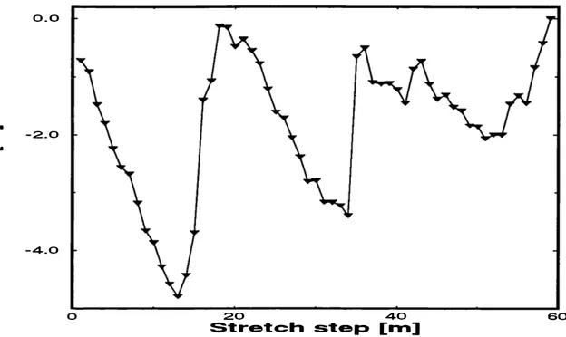
4.3. MD-RESULTS FOR Cu(lll) NANOWIRE
Except for some minor changes, the stretch of nanowire made from Cu( 111)
layers ( as specified by
W
N2 in Fig.4) has overall features of the yielding
mechanism at T
=
300K, which are similar to the above Cu(OOl) orienta
tion. In Fig.7, we show the force variation with stretch. The force curve
depicts consecutive elastic and yielding stages. The elastic stages prior to
the first and second structural transformation are rather linear with strain.
This is not so in the third stage before the break, where either the structure
becomes disordered or changes the registry from the H- to T-site. In fact,
after few stretch steps, the magnitude of F
zdrops suddenly due to onset of
disorder without formation of a new layer. During the last stage of stretch,
the strain is almost accommodated by the layers at the central part of the
neck. The 2D hexagonal-like structure is quite robust for the layers adjacent
or close to the end layers M
3and
M
4•Here the A-B-C stacking sequence
226
0 . 0Z
- 2 . 0 ..!::... f:::!&
- 4 . 0 20 40 60 Stretch step [m]Figure 7. The variation of the tensile force F z with the stretch along the z-axis for Cu(OO I ) nanowire
(W
N2) atT
=
300K.
and the H-site registry are forced by these end layers. In the central part of the neck, the distortion of the 2D hexagonal lattice structure becomes severe and the A-B-C sequence disappears, but the H-site registry is kept after the yielding stage. However, the atomic chains form as a result of the transition to the T-site registry in the last stage of stretch.
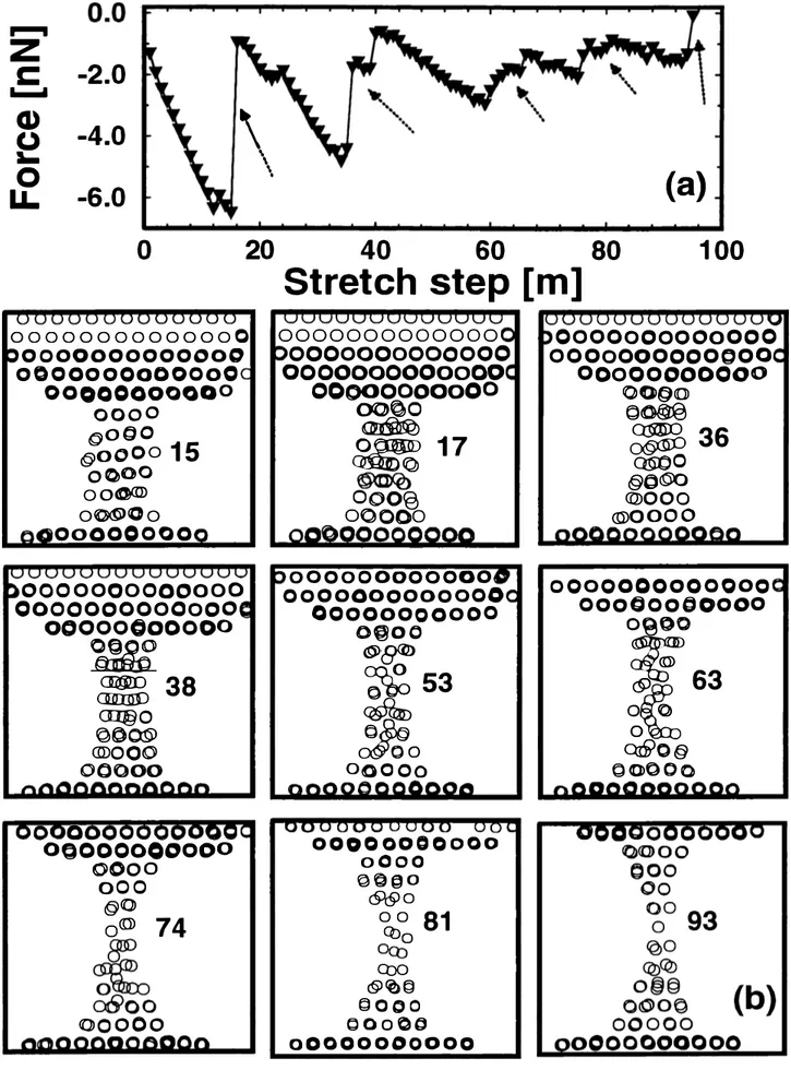
If
the same Cu(lll) wire is stretched at low temperature(T
=
150K),it exhibits features, some of which are dramatically different from those at room temperature. For example, the same wire undergoes
five
yielding stages resulting in an elongation of 9 . 5.A; whereas at room temperature, it had onlythree
yielding steps with6.A
elongation. Apparently, while the necking is faster and sharper and hence, it is more trumpet-like at room temperature, the neck is longer at low temperature. We explain this with faster atomic motion towards the ends of the wire at room temperature. Another feature which does not exist at room temperature is a new type of structural transformation. The F z( m) curve and some relevant side views of the wire in Fig.8 distinguish different types of yielding mechanisms. The first and second yielding stages are similar to the previous cases in which the structure undergoes layer-disordered-layer transformations during the generation of a new layer. Atm
=
15 a well-defined layer structure becomes broader and slightly disordered, and a new layer forms atm
=
16. This yielding stage occurs more abruptly with least necking; the size of the layers decreases by 2- 3 atoms. Similar process repeats atm
=
3 5, and creates a new layer atm
=
3 6. Again, in this process most of the layers are affected and reduced by two atoms with no significant necking effect. The hexagonal...
z
C
...
G)
E
0
u.
-2.0
-4.0
-6.0
\
(a)
0
20
40
60
80
1 00
0 0 0 0 0 0 0 0 0 0 0 0 0 0 0 0 00000000000 0 0 0 00 0000 00 00 00000000000 0 0 0 0 00 0 0 §0 0 0 0 1 5 0 000ooo«D
oc:Mi>O o
00000 0 0 0000 0000000000
0000000000000
00000000000
°@Wft
aW)38
<El]l) Cll§O�o�
CIDOOO 000000
00000000000
000 0 oO O §0 a@74
00 0 0 0Stretch step [m]
0 0 0 0 0 0 0 0 0 0 0 0 00000000000000
0000000000000
00000000000
=
= 1 7
OOO@ 00 000 0 0 0 0 0 000 0 000 0 0 0 0000000 000 0000000 00 00 0@0 0�cl!'
� 53
�
ofiD§
oOo o
00 0 0 0 0 0 0 0 00 0 0 0 0 0 0 0 0 0 o o g o@@o
0 081
Cbo QJO @ % § Q O C, O 0 0 0 0 0 0 0 0 0 0 0 0 0 0 0 00000000000000
0000000000000
00000000000
OOQI[])
0�
� 36
Q§OO §000 (0)000 <!DO OO O 0 00000000 0 000 000 0 0 0 0 0000�
1
63
0 0 0afro@
0 00 0 0Figure 8. (a) Variation of the tensile Force F z with the stretch for the Cu{l l l ) nanowire
(W
N2) atT
=
1 50K. We mark the yielding stages by arrows. (b) The side views of the structure at some relevant stretch steps m.228
m=53
m=66 0
m=81
0 �
+
O
+
'
o +
+ ' 4>
i , +
0
+
o+
0
0
'
+o
*
'
O
+
O
''
'n4,n5
n6,n7
n6,n7
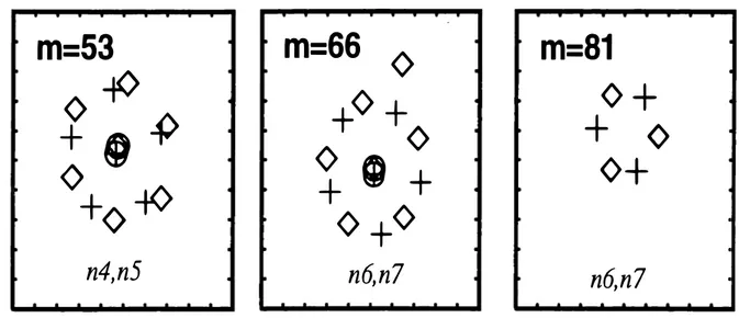
'Figure 9. Atomic positions of adjacent layers at the neck center in the (xy)-plane for some relevant stretch steps described in Fig.8. The atoms of the adjacent layers indicated by n 's are shown by
+
and O , respectively. The atoms situated in the space above these layers are circled.rings a.nd A-B- C stacking sequence of the Cu(lll) planes a.re robust nea.r the end layers
( M
3 a.ndM
4). At the centra.l la.yers hexa.gona.l rings persist,but the A-B- C stacking sequence a.nd its cha.ra.cteristic registry between a.dja.cent layers are destroyed. The shape of the layers in the (xy ) -pla.ne is distorted. For
m
>
39, a.n intermediate situation occurs within elastic stages: Hexa.gona.l rings change into penta.gona.l ones; the latter becomes staggered to the rings in the a.dja.cent layers. Moreover, one layer a.t a. time ( starting from the centra.l la.yer) ejects a. single a.tom to the interlayer space. This wa.y a. column ( or cha.in) of a.toms is formed a.long the a.xis of the neck. The projection of this cha.in in the (xy
) -plane is almost a. single point nea.r the centers of penta.gona.l rings a.s shown in Fig.9. Out offive
yielding stages, the la.stthree
ha.ve this feature. At prolonged stretch ( m>
75), the number of a.toms in the neck layers a.re reduced a.nd the layer structure becomes more distorted; staggered pentagonal rings change into tria.ngula.r ones a.gain with staggered orientation. A few steps before break ( 8 4<
m
<
9 4), a. single atomic cha.in forms eventually. We understand tha.t a.t low temperatures, the mobility of a.toms a.re not suitable for massive changes, so the neck ca.n a.ccommoda.te the applied strain by these new intermediate structures which require least atomic rea.rra.ngement.5. Mechanical properties of nanowires
To reveal physical phenomena. underlying the "giant" Young's modulus ob served in thin wires shortly before the break we carried out
ab initio
ca.lcu la.tions by using SCF pseudopotentia.l method within local density a.pproxi ma.tion. The effective force constant keJ f , tha.t is defined a.s the mecha.nica.l force per elongation ca.n be estimated from the slope of the curve Fz(m). Fora contact , the effective force constant is given by k
eff=
R7E/( l - v)
2(see
Ref. 12 and 29) . Here
R,
'Y ,
E
and v are respectively contact radius, a factor
describing the exact distribution of stress, Young's modulus and Poisson's
ratio. From F z versus displacement curves measured by the combined STM
and AFM , Agrai"t et al.[12] obtained k
eJJ= 240N/m and R
rv3nm. Using
the above contact expression of k
,,1 f , they estimated E
rv66 - 44 G Pa
which is consistent with the macroscopic value of the Young's modulus
of Au. On the other hand, Stalder and Diirig[13] found that the intrinsic
yield strength of a neck with R
rv1 nm ( corresponding to a crossection
A
"' 300.A.
2) between the Au( l l l ) sample and Au tip is 8 GPa, which
is one order of magnitude larger than the macroscopic value. This value
approached to 20GPa shortly before the break. The discussions in the pre
vious section point to the fact that in the last steps of the stretch, where
the neck is reduced to 1 - 3 atoms, either the bundle of atomic chains
or single atomic chain is formed. This structure of the neck is rather dif
ferent from the original structure derived from the atomic arrangement
of the macroscopic bulk and is expected to lead dramatic changes in the
mechanical properties. For example, the observed "giant" yield strength
may originate from the unusual changes in the structure. By definition, the
yield strength ay is the stress, a = F z/
A
at the yield point where the
linear relation between stress and strain starts to break. Since ay = EEy
( Ey being the strain at the yield point), the observed "giant" yield strength
may be due to high strain value and/or high Young's modulus attained by
atomic chain. As a matter of fact , owing to the transition from the H-site
registry to the T-site registry, a neck can attain large values[28,30] for Ey .
Moreover,
ab initio
calculations that we discuss below demonstrate that
E
also increases in the neck consisting of atomic chain. Of course, the yield
strength and Young's modulus are definitions, which are developed within
the continuum description of matter. By adopting some of the variables
(such as the crossection
A)
in these definitions we attempt to calculate
E
in the quantum limit .
The Young's modulus of an atomic chain can be expressed by E
=
kb/A,
where k is the force constant and b is the interatomic distance. Apparently,
the size and dimensionality of the chain go beyond the limits of continuum
description, and the estimation of
k
requires
ab initio
quantum mechanical
calculations. To this end, we carry out total energy calculations by using
SCF pseudopotential method in momentum representation. Accordingly,
we take into account the infinite Al-chain whereby we can use periodic
boundary condition and pseudopotentials which converge easily for a sim
ple metal. For example, by using the kinetic energy cut-off J k + GJ <
7.5Ry,
one can achieve accurate representation of the wave function and band en
ergies. As pointed earlier[28,30] , a short Al-chain can form in an Al-neck.
230
Moreover, the mechanical properties _of a short Al-chain can be revealed from those of infinite chain. We use non-local and norm-conserving pseu dopotentials[31] with Wigner exchange-correlation potential. We treat the
lD
infinite atomic chain in a3D
supercell geometry in which the inter chain distance is taken 7. 5.A. The minimum total energy is obtained forb
=
2.403.A. The force constantk
is obtained from the variation of total energy relative to interatomic distanceb,
i.ek
=
- 82Er(b)/ab
2, and isfound 164N /m. There are ambiguities in the definition of crossection; here we used two schemes which yield similar values: i) A
=
0.3811" A} which is the crossection necessary to open a ballistic conduction channel within free electron and infinite wall cylindrical potential approximation.ii )
A=
11" R2;here R is the radius at the value of calculated SCF potential, which is equal to EF, For Al, we find A = 15.38.A.2 at T
=
3001( from the first scheme, andA "' 14.0A.2 from the second scheme. Eventually, we calculate the Young's
modulus of Al-chain,
E
"' 260GPa
which is approximatelyfour
times larger than the bulk value. This implies that the mechanical properties of metal chain or bundle structure is different from those of bulk values, as well as from those of the neck or metal wires having large crossection, such asA
"' 300.A.2 as in the experiment[13]. The raise ofE
upon bundle orchain formation may have dominant contribution to the observed "giant" yield strength.
6 . Discussion
Our calculations of the conductance for the idealized and circularly sym metric constriction fail to explain the experimental results. In view of this we investigated the effect of the atomic rearrangements induced by the tensile force. Our analysis based on the state of the art molecular dynam ics simulations using the embedded atom potential show that the yielding and fracture mechanisms of a nanowire under uniaxial tensile force depend on atomic structure and temperature, and also on the pulling conditions. There are, however, features which are common to all nanowires under uni axial strain. The important aspects of the present study are summarized: 1 . Deformation ( or elongation) in two different stages, that occur consecu tively and repeat until fracture, are common to all nanowires treated in this study. In the first stage, the stored strain energy and average tensile force increase with increasing stretch, while the layer s tructure persists. Exclud ing the :fluctuations (possibly due to displacement and relocation of atoms within the same layer or atom exchange between adjacent layers) , the vari ation of
F
z ( m) is approximately linear. This stage was identified as elastic.Once the elongation of the nanowire reaches the interlayer separation at the end of the elastic stage, the structure becomes disordered; but after a
few increments of stretch, it is recovered with the formation of a new layer.
In this yielding stage,
IF
z
I
decreases abruptly; the crossection of narrowest
neck layers that determines the conductance, in particular the crossection
of the layer formed at the end of yielding stage are reduced abruptly by
a few atoms. W hen the neck becom es very narrow (having 3-4 atoms) the
yielding is realized, however, by an atom jumping from one of the adjacent
layers to interlayer space. On the other hand, it may occur through slips or
the motion of dislocations when the wire is much wider. At low tempera
ture, the yielding takes place in relatively shorter time-interval within one
or two stretch steps. Owing to the limited mobility of atoms at low temper
ature, the character of elastic stage changes if the neck is long enough.
In
this situation, each layer ejects one atom to the adjacent interlayer space as
it widens with the applied strain. The layers at the neck are made from the
pentagon rings which become staggered in different layers. The interlayer
atoms make a chain passing through the center of pentagon rings.
In
this
new phase, the elastic and yielding stages are intermixed and elongation
which is more than one interlayer distance can be accommodated.
2. In the initial steps of stretch, the layered structure and ordered 2D
atomic arrangement within the layers are maintained. Upon increased uni
axial strain (increased m), the layers become wider and rougher due to the
atoms departing from the atomic plane, the 2D lattice is distorted, and
interatomic distances start to deviate from the bulk equilibrium value.
In
the elastic stage, one can still distinguish layer structure and some kind of
order in the atomic arrangement within a layer. In particular, the hallow
site registry between layers are maintained if the layers contain enough
number of atoms. The ordered atomic arrangement becomes disordered at
low temperature towards the end of stretch.
3. The elastic and following yielding stages are reminiscent of the stick
slip motion. In the course of stretch, elastic and yielding stages repeat;
the surface of the nanowire roughens and deviates strongly from circular
symmetry. The narrowest part, which is only a layer thick, is connected
to horn-like ends. Our results of atomic simulations point to the fact that
neither adiabatic evolution of discrete electronic states, nor circular symme
try induced degeneracy can occur in the neck . Consequently any quantized
sharp structure shall be smeared out by channel mixing and tunneling[9] .
On the other hand, owing to the sudden reduction of crossection by a few
atoms, some states contributiong to current carrying states are eliminated
suddenly. This leads to sudden drop of
G
with stretch as described by
dashed line in Fig3-b.
4. In addition to the stick-slip behavior under strain, atoms also migrate
in a much slower process. The migration process speeds up with increasing
temperature and its effect on necking becomes significant when a thin neck
232
has a canonical connection to the ends. Also a transient and permanent exchange of atoms between adjacent layers can take place. This may lead to transient dips on spikes in the G(
s)
curve.5 .
If
the interlayer interaction is reduced as a result of extensive strainthe 2D atomic structure (square-like lattice) is transformed into hexago nal rings. At prolonged stretch, just before the the break, the crossection of layers at the central part of the neck is reduced to 2 - 3 atoms. In this case, the H-site registry may change to the T-site registry. This leads to the formation of bundle of atomic chains or single atomic chain. We consider this a dramatic change in the atomic structure of the wire and may have important implications. The positive slope of G(
s)
curve at the last plateau of Al can be explained by the chain formation[30 ].6 . Our
ab initio
calculations of Young's modulus on theID
metal chains indicate that the neck having chain structure may have yield strength much higher than the bulk value. This is in good agreement with experimental results[3,12,13 ], and also implies that the elastic properties of an atomic size neck deviate from those of the bulk defined in the continuum limit.In conclusion, the simulations of atomic structure in nanowires under tensile stress indicate novel mechanisms of plastic deformation and elonga tion. When the restoring effect of the initial structure is weakened under the applied uniaxial force, the atomic arrangement deviate from the global minimum and can be stabilized in a different local minimum. The corre sponding configuration exhibits a non-crystalline, short-range order and interesting mechanical and transport properties induced thereform.
Acknowledgements
We would like to thank Prof. M. S. Daw for providing embedded atom potential for Cu and Dr. E. Tekman, Prof. � - Erkoi; and Dr. B. Tanatar for helpful discussions.
References
1 . For extensive review see: ( 1 99 1 ) J . L . Beeby(eds . ) , Condensed Systems of Low Di
mensionality, N ATO ASI Series B , Phys . Vol. 2 5 3 , Plenum Press ; ( 1 9 9 1 ) L . Esaki (eds . ) , Highlights in Condensed Matter Physics and Future Prospects, N ATO ASI Series B, Phys. Vol. 2 8 5 , Plenum Press.
2. Gimzewski, J . K . and Moller, R. ( 1 98 7 ) Transition From the Tunneling Regime to Point Contact Studied by Scanning Tunneling Microscopy, Phys. Rev. B36 , 1 2 84- 1 2 8 7 .
3 . Landman , U . , Luedtke, W. D . , Burnham , N . A . and Colton , R . J . ( 1 99 0 ) Atomistic M echanisms and Dynamics of Adhesion, N anoindentation and Fracture, Science 248 , 454-46 1 .
4 . Agra.it , N . , Rodrigo, J . G . and Vieiria, S . ( 1 9 9 3 ) Conductance Steps and Quanti zation in Atomic-Sized Contacts, Phys. Rev. B47 , 1 2345- 1 2348.
5 . Pascual, J . I . , M endez , J . , Gomez-Herrero, J . , Baro, A . M . , Garcia, N . and Bin h , V . T. { 1 9 9 3 ) Quantum Contact i n Gold Nanostructures b y Scanning Tunneling Microscopy, Phys. Rev. Lett. 71, 1 8 5 2- 1 8 5 5 ; Pascual, J . I . , Mendez, J . , Gomez H errero, J . , B aro, A. M . , Garcia, N . , Landman , U . , Luedtke, W . D . , B ogachek, E . N . and Cheng H . P. ( 1 9 9 5 ) , Properties of Metallic N anowires: From Conductance Qu antiz ation to Localization , Science 267, 1 7 93- 1 7 9 5 .
6 . Olesen , L . , L aegsgaard, E. , Stensgaard, I . , Besenbacher, F . , Schiflltz , J . , Stoltze, P. , J acobsen , K.W. and Nfllrskov, J . K. { 1 994) Quantization Conductance in an Atom-sized Point Contact , Phys. Rev. Lett. 72, 2251-2254; { 1 9 9 5 ) Olesen et al . Reply, Phys. Rev. Lett. 74, 2 1 47- 2 1 4 7 .
7. K rans, J . M . , M iiller, C . J . , Yanson, I . K . , Gowaert, Th. C . M . , Resper R. and Ruiten beek, J . M . { 1 9 9 3 ) One Atom Point Contact, Phys. Rev. B48, 1 4 7 2 1 - 1 4724.
8. Ciraci, S . and Tekman , E. { 1 9 8 9 ) Theory of Transition from the Tunneling Regime to Point Contact in S canning Tunneling Microscopy, Phys. Rev. B40 , 1 1 9 6 9-1 9-1 97 2 ; Ciraci, S . { 9-1 9 9 0 ) Tip Surface Interactions, in R. J . Behm, N . Garcia and H . Rohrer(eds . ) , Scanning Tunneling Microscopy and Related Methods, Kluwer Aca demic Publishers , Volume 184, pp. 1 1 3- 1 4 1 .
9 . Tekman , E . and Ciraci, S . { 1 9 9 1 ) Theoretical Study o f Transport through a Quan tum Point Contact , Phys. Rev. B43 , 7 1 45-71 6 9 .
1 0 . Todorov, T. N . and Sutton, A . P. { 1 9 9 3 ) Jumps i n Electronic Conductance d u e to M echanical Instabilities, Phys. Rev. Lett. 70, 2 1 38-2 1 4 1 .
1 1 . K rans, J . M . M iiller, C . J . , Van der Post , N . , Postama, F . R. , Sutton , A . P . , Todorov, T . N . and Ruitenbeek, J . M . { 9 9 9 5 ) Comments on Quantized Conductance in an Atom-sized Point Contact , Phys. Rev. Lett. 74, 2 1 46-2 1 4 6 .
1 2 . Agra.i:t , N . , Rubio , G and Vieiria, S . { 1 9 9 5 ) Plastic Deformation o f N anometer-Scale Gold Connective Necks, Phys. Rev. Lett. 74, 3 9 9 5- 3 9 9 8 ; Rubio , G . , Agra.i:t , N. and Vieiria, S. { 1 9 9 6 ) Atomic-sized Metallic Contacts, Phys. Rev. Lett. 76, 2 3 0 2- 2 3 0 5 . 1 3 . Stalder, A . and Diirig, U . { 1 9 9 6 ) Study of Yielding Mechanics in N anometer-sized
Au Contacts , App . Phys. Lett. 6 8 , 6 3 7- 6 3 9 .
1 4 . Landauer , R. { 1 957) Spatial Variation o f Currents and Fields due t o Localized scatterers in Metallic Conduction , IBM J. Res. Develop . I, 223-23 1 .
1 5 . Sharvin , Yu . V . { 1 9 6 5 ) A Possible Method for Studying Fermi S urfaces , Zh. Eksp.
Tear. Fiz. 4 8 , 984- 9 8 5 ; [Sov. Phys. - JETP 2 1 , 655-656] .
1 6 . Van Wees , B . J . , Van Houten , H . , Beenakker, C . W . J . , Williamso n , J . G , Kouwen hoven, L . P. , van der M are!, D. and Foxon , C . T . ( 1 9 8 8 ) Quantized Conductance of Point Contacts in a Two- Dimebsional Electron Gas, Phys. Rev. Lett. 6 0 , 848- 8 5 0 . 1 7 . Wharam , D . A . , Thorton, T. J . , Newbury, R. , Pepper, M . , Ahmed , M . , Frost , J . E. F , Peacock, D . G . , Ritchie, D . A . and Jones, G . A . C . { 1 9 8 8 ) One-Dimensional Trans port and the Quantization of the Ballistic Regime, J. Phys. C2 1 , L209- L 2 1 4 . 1 8 . B iittiker, M . , Imry, Y . , Landauer, R. and Pinhas, S . { 1 9 8 5 ) Generalized M any
Channel Conductance Formula with Application to Small Rings, Phys. Rev. B3 1 , 6207-6 2 1 5 ; Imry, Y . { 1 9 8 6 ) Physics of Mesoscopic Systems, in G . Grinstein and G . M azenko { eds . ) , Directions i n Condensed matter Physics, World Scientific Publisher, Singapore, pp. 1 0 1 - 1 6 3 .
1 9 . Been akker, C . W . J and van Houten , H . { 1 9 9 1 ) Quantum Transport i n S emiconduc tor N anostructure, in H . Ehrenreich and D . Turnbull(eds . ) , Solid State Phys.44, Academic Press, Inc. , pp . 1- 1 7 0 .
2 0 . Lang, N . D . { 1 987) Resistance o f a One-Atom Contact i n t h e Scanning Tunneling Microscope, Phys. Rev. B3 6 , 8 1 73-8 1 76 .
2 1 . Ferrer , J . , M artin- Rodero, A . and Flores, F . { 1 9 8 8 } Contact Resistance i n the Scaaning Tunneling Microscope at very small Distances , Phys. Rev. B38 , 1 0 1 1 3-1 0 3-1 3-1 5 .
2 2 . D aw , M . S . and Baskes , M . I . { 1 984) Embedded-atom Method: Derivation and Ap plication to Impurities, Surfaces and Other Defects in Metals, Phys. Rev. B29, 6443-645 3 .
234
23. Foiles, S . M . , Baskes, M.I. and Daw, M.S. {1986) Embedded-atom Method functions for the FCC Metals "Cu, Ag, Au, Ni, Pd, Pt and their Alloys, Phys. Rev. B33, 7983-799 1 .
24. Daw, M.S. {1 989) Model of Metallic Cohesion: The Embedded-atom Method, Phys.
Rev. B39, 7441-7452.
25. Lynden-bell, R.M . {1 994) Computer Simulations of Fracture at the atomic level, Science 263, 1704-1705.
26. Bratkovsky, A.M, Sutton, A.P. and Todorov, T.N . {1 995) Conditions for Conduc tance Quantization in Realistic Models of Atomic-scale Metallic Contacts, Phys.
Rev. B52, 5036-5051 .
27. Mehrez, H . , Ciraci, S. and Erko�, �- { 1997) Yielding and Fracture Mechanisms of Nanowires, Phys. Rev. B (to be published) .
28. Ciraci, S., Baratoff, A. and Batra, I.P. {1 990) Site-dependent Electronic Effects, Forces and Deformation in Scanning Tunneling Microscopy, Phys Rev. B42, 7618-762 1 , for Al{ l l l ) surface; and Ciraci, S., Tekman, E., Baratoff, A. and Batra I.P. {1 992) Theoretical Study of Short- and Long- Range Forces and Atom Transfer in Scanning Tunneling Microscopy, Phys. Rev. B46, 1 0411-10422, for Al{OOl) surface. 29. Johnson, K.L. {1 986) Contact Mechanics, Cambridge University Press, Cambridge. 30. Mehrez, H., Ciraci, S., Buldum, A. and Batra, I.P. {1 997) Conductance through a
Single Atom, Phys. Rev B55.
31. Bachelet, G.B., Hamann, D.R. and Schliiter, M. {1 982) Pseudopotentials that work from H to Pu, Phys. Rev. B26, 41 99-4228.