Confinement of electrons in size-modulated silicon nanowires
S. Cahangirov1and S. Ciraci1,2,*
1UNAM–Institute of Materials Science and Nanotechnology, Bilkent University, Ankara 06800, Turkey 2Department of Physics, Bilkent University, Ankara 06800, Turkey
共Received 3 March 2009; revised manuscript received 3 June 2009; published 12 August 2009兲
Based on first-principles calculations we showed that superlattices of periodically repeated junctions of hydrogen-saturated silicon nanowire segments having different lengths and diameters form multiple quantum-well structures. The band gap of the superlattice is modulated in real space as its diameter does and results in a band gap in momentum space which is different from constituent nanowires. Specific electronic states can be confined in either narrow or wide regions of superlattice. The type of the band lineup and hence the offsets of valence and conduction bands depend on the orientation of the superlattice as well as on the diameters of the constituent segments. Effects of the SiH vacancy and substitutional impurities on the electronic and magnetic properties have been investigated by carrying out spin-polarized calculations. Substitutional impurities with localized states near band edges can make modulation doping possible. Stability of the superlattice structure was examined by ab initio molecular-dynamics calculations at high temperatures.
DOI:10.1103/PhysRevB.80.075305 PACS number共s兲: 73.63.Nm, 73.22.⫺f, 75.75.⫹a
I. INTRODUCTION
Rodlike Si nanowires 共SiNW兲 have been synthesized down to ⬃1 nm diameter.1 They are attractive one-dimensional materials because of the well-known silicon fab-rication technology that make them directly usable on the Si-based chips. Even if unsaturated dangling bonds on the outer surface usually attribute a metallic character to SiNWs, they become insulator共or semiconductor兲 upon saturation of these dangling bonds by hydrogen atoms.2 SiNWs display diversity of electronic properties depending on their diameter as well as their orientation. In particular, the band gap of semiconductor SiNWs varies with their diameters. They can be used in various electronic, spintronic, and optical applica-tions, such as field-effect transistors,3light-emitting diodes,4 lasers5and interconnects. The conductance of these semicon-ductor nanowires can be tuned easily by doping6,7during the fabrication process or by applying a gate voltage. Recent studies have shown that 3d transition-metal-doped Si nano-wires become half metallic.8
This paper demonstrates that SiNWs of different diam-eters can form stable superlattices. The electronic band structure of the superlattice is different from the consti-tuent SiNWs and is modulated in real space leading to a multiple quantum structure and/or to a series of quantum dots. In these size-induced quantum wells, specific states are confined. One-dimensional multiple quantum-well struc-tures generated by compositional modulation of nanowires were examined previously. For example, superlattices of GaAs/GaP,9 InAs/InP,10 and Si/SiGe 共Ref. 11兲 nanowires were fabricated. Moreover, superlattices of Si and Ge were investigated theoretically.12In these structures multiple quan-tum wells are formed because of the different nature of ma-terials that constitute the nanowire superlattice. In the present work however, multiple quantum wells are formed because of the quantum-size effect, which is a diversification of the electronic structure of the same material with a change in its size.
Our results are obtained by performing first-principles plane-wave calculations within density-functional theory
共DFT兲 共Ref. 13兲 using ultrasoft pseudopotentials.14,15 The exchange-correlation potential has been approximated by generalized gradient approximation using PW91 functional.16A plane-wave basis set with kinetic-energy cut-off of up to 250 eV has been used. All atomic positions and lattice constants are optimized. The convergence for energy is chosen as 10−5 eV between two steps and the maximum force allowed on each atom is 0.02 eV/Å. More details about calculations can be found in Ref8.
II. SIZE-MODULATED SILICON NANOWIRES Here Si nanowires共i.e., SiN1with diameter⬃D1and hav-ing N1Si atoms in the primitive unit cell兲 are first cut from the ideal bulk crystal along desired direction. Then in every alternating segment comprising l1unit cell the diameter D1is kept fixed but in the adjacent segment comprising l2unit cell 共each having N2Si atoms兲 the diameter is reduced to D2. The latter part can be identified as the segment of SiN2nanowire. At the end, the segments of SiN1 and SiN2 have made a smooth junction and hence formed an ideal superlattice SiN so that its diameter is modulated in real space. Note that N ⱕl1N1+ l2N2 because some surface atoms attaching with a single bond to the surface were removed at the beginning. Subsequently we relaxed the atomic structure of this bare SiN. Upon relaxation, the dangling bonds on the surface are saturated by H atoms and SiNHM superlattice is further re-laxed for final atomic structure and the lattice constant. The resulting superlattice can be described by a Si rod with alter-nating diameters or a nanowire with alteralter-nating wide and narrow parts. Here we consider two superlattice structures, namely, Si138H42and Si157H64, which are grown in关111兴 and 关100兴 directions, respectively. For the latter we investigate the surface defect and also boron, B and phosphorus, P sub-stitutional impurities.
A. Si138H42superlattice
To form the superlattice, Si138H42, we took l1= 1 unit cell of Si68and l2= 2 unit cell of Si38cut in关111兴 direction of the
bulk silicon crystal. The combined structure had six Si atoms attached to the surface by only one bond. These atoms were removed at the beginning and the structure was optimized. After the relaxation, all Si atoms were at least triply coordi-nated. The dangling bonds of triply coordinated Si atoms were saturated with hydrogen atoms and the structure was relaxed again. The band structure and isosurface charge den-sities of the resulting superlattice is shown in Fig.1. Propa-gating states with dispersive bands have charge densities dis-tributed everywhere in the superlattice rod. For example, a state near⬃−1 eV is a propagating state. The states of flat degenerate band at the top of the valence band are confined in the narrow segment. The integral of the planarly averaged charge, 兰l1兩⌿共z兲兩2dz = 0.96 indicates a rather strong confine-ment. The states of the lowest conduction band with low dispersion are localized in the wide segment with relatively weaker confinement. This situation implies the staggered band alignment with confined hole states in the narrow part and confined electrons in the wide part. Confinement may increase with the size共length兲 of the confining segment since the energy of the state relative to the barrier varies. For per-fect localization, i.e.,⬃100% confinement in l1or l2, where coupling between confined states are hindered, the segment
l1 or l2 behaves as a quantum dot. Confinement and band-edge alignment in the present superlattice are reminiscent of the two-dimensional pseudomorphic or commensurate semi-conductor superlattices.17
B. Pristine Si157H64superlattice and vacancy
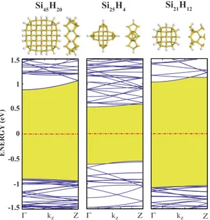
Here we presents the superlattice formation and confined states in a different structure, namely, Si157H64. To form this structure we took l1= 2 unit cell of Si45and l2= 3 unit cell of Si25 cut in 关100兴 direction of the bulk silicon crystal. The combined structure had eight silicon atoms that were at-tached to the surface by only one bond. We have removed these atoms at the beginning and relaxed the resulting struc-ture. Then we have passivated the dangling bonds of the final structure and relaxed the whole structure again. As a result, the wide part of the nanowire superlattice had l1= 2 unit cell of Si45H20 with D1⬃14 Å and the narrow part had l2 = 3 unit cell of Si25H4 and Si21H12 mixture with D2⬃7 Å. Figure 2 presents the band structure of the corresponding infinite periodic nanowires which constitute the Si157H64 su-perlattice structure. To compare with the band structure of the superlattice 共presented in Fig. 3 as pristine兲, the band
structure of these nanowires were folded l1+ l2= 5 times. One can see that the band gap of the superlattice is close to the lowest band gap of its constituents. This is expected for the superlattice structures having normal band lineup. The band gaps of structures shown in Fig. 2 do not obey the well-known trend, EG= C/D␣+ EG关bulk Si兴, occurring due to the quantum-confinement effect18 at small D. We ascribe this result to the surface reconstructions which differ in accor-dance with the procedure of atomic relaxation. Quantum-confinement trend occurs when Si nanowires, cut from ideal bulk, are directly passivated with H atoms and subsequently relaxed. In the present study, however, the ideal structures are first relaxed, then passivated with H atoms, and then relaxed again to obtain the final structure.8Such Si nanowire structures with D⬃1 nm may not obey the
quantum-ENERGY (eV) 1 -1 0 0.5 -0.5 Γ kz Ζ Si138H42
BAND CHARGE DISTRIBUTION
l
1l
2[111]
73% 27%
4% 96%
34% 66%
FIG. 1. 共Color online兲 Energy-band structure of the superlattice, Si138H42, formed from periodically repeated junctions consisting of one unit cell of SiNW with D1⬃11 Å and two unit cell of SiNW with D2⬃7 Å formed along 关111兴 direction. Here the diameter D is defined as the largest distance between two Si atoms in the same cross-sectional plane. Isosurface charge densities of specific bands and their planarly averaged distribution along the superlattice axis together with their confinement in percentages are also shown. Large and small balls indicate Si and H atoms. Zero of energy is set at the Fermi level shown by dash-dotted line.
ENERGY (eV) Γ kz Ζ Si45H20 Γ kz Ζ 1 -1 0 0.5 -0.5 -1.5 1.5 Si25H4 Γ kz Ζ Si21H12
FIG. 2. 共Color online兲 Band structures of infinite and periodic Si45H20, Si25H4, and Si21H12nanowires, which constitute Si157H64 structure. The front and side view of these relevant structures are shown on the top of the band-structure plots. Numerals as sub-scripts of Si and H indicate the number of Si and H atoms in the unit cell. Energy-band gaps are shaded.
confinement trend. The decline of the gap values from the 1/D␣ behavior has been also reported for other types of SiNWs and was attributed to surface effects.19
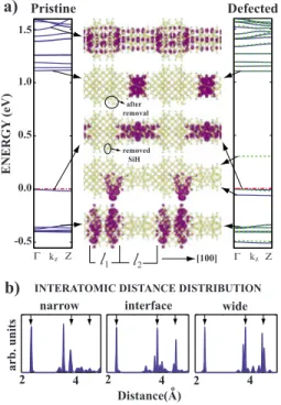
Figure 3共a兲presents the band structure and the projected charge-density isosurface plots of pristine Si157H64 and de-fected Si156H63 nanowire superlattices. Flat minibands of Si157H64 structure near the edge of conduction and valence bands are distinguished.17In contrast to propagating states of dispersive bands near 1.5 eV, the states of these flat mini-bands are confined in the narrow segments of the superlat-tice. This situation also implies a normal band lineup. We are aware of the fact that fabrication of nanowire superlattices having ideally tapered as in our case is impossible. So we examined the effect of an imperfection on the behavior of the system by removal of a Si-H atom pair, which was normally attached to the surface. The location of this defect and struc-tural change after relaxation is given in Fig.3共a兲. The result-ing structure has odd number of electrons, so we made spin-polarized calculation. One can see that the valence- and conduction-band edges are not affected by defect formation while one empty and one filled state localized around the defected area appear near the valence-band edge. The mag-netic moment induced by the defect formation is 1B. The vacancy states in bulk Si are located deep in the band gap. In the superlattice structure, this vacancy state is located near
the valence band since the defect is formed on the surface at the interface between two segments having different diam-eters.
In Fig. 3共b兲 the distribution of interatomic distances shows significant reconstruction and deformation. In particu-lar, owing to increased surface/volume ratio the deviation of the second- and third-nearest-neighbor distances from the bulk crystal is rather large at the narrow and interface re-gions. We note that in both short periodicity superlattices discussed above the electronic structures are significantly different from the constituent SiNWs. As l1 and/or l2 in-creases, the superlattice effects and confined states may be-come more pronounced, and band offset converges to a well-defined value. When the lengths of l1 and l2⬎B 共Broglie wavelength兲, the electronic properties in each segment be-comes close to those in constituent nanowires. In addition to
l1and l2, D1and D2and also the direction of growth are also critical parameters, since the electronic structure of the con-stituent SiNWs is strongly dependent on these parameters. As D1and D2increases, the surface effects decrease and the density of states becomes more bulklike. The discontinuities of valence and conduction bands of the superlattice is ex-pected to diminish since the band gap of the constituent nanowires converge to the bulk Si value. However for a sig-nificant ⌬D=D1− D2 the superlattice effects, in particular, confinement of specific states are expected to continue. In contrast, smooth interfaces leading to hornlike profiles can be used for focused electron emission.20 Recently, transport properties of size-modulated SiNWs have been shown to de-pend on the growth direction.21
The stability of the Si157H64structure was analyzed using the finite-temperature ab initio molecular-dynamics calcula-tions with time steps of 2⫻10−15 s. Figure4共a兲presents the total-energy difference of the system with respect to the ground-state energy at 0 K as a function of time. In the first calculation we have raised the temperature of the system from 500 to 1400 K in 2 ps. During this calculation there was no major change in the structure and the interface region was not destroyed by diffusion. In the second calculation we took atomic positions and velocities of the system from the first calculation when the system was at 1300 K and kept the temperature constant for 9 ps. This calculation also resulted in no major change in the structure of the superlattice. Fig-ures 4共b兲 and 4共c兲present the path of Si atoms during the second calculation at the surfaces of wide and narrow parts, respectively. The range of the thermal fluctuations are nearly the same and span a diameter of about 1 Å. Figures4共d兲and
4共e兲present the path of Si atoms at the center of the wide and narrow parts, respectively. As seen the range of thermal fluc-tuations in the narrow part共⬃0.9 Å兲 is larger than that in the wide part 共⬃0.5 Å兲. It should be noted that, the temporal trajectories of 9 ps in the present ab initio molecular-dynamics calculations are rather long as compared to ones usually carried out in the stability tests but may not be long enough to accumulate necessary statistics. However, the tem-poral trajectories at temperature as high as 1300 K in the present study are long enough to eliminate the existence of any atomic configuration in a weak local minimum of the Born-Oppenheimer surface, which is prone to structural in-stability. Therefore, based on the accurate structure
optimi-1.5 0.5 0.0 1.0 -0.5 ENER G Y (eV ) Γ kz Ζ [100] a) b) arb. units wide interface narrow Distance(A)o 2 4 2 4 2 4
INTERATOMIC DISTANCE DISTRIBUTION
l
1l
2 Γ kz Ζ Pristine Defected removed SiH after removalFIG. 3. 共Color online兲 共a兲 Electronic structure and isosurface charge densities of selected states for pristine Si157H64and defected Si156H63共with one Si-H on the surface removed兲 nanowire super-lattices. Arrows pointing at the same isosurface charge-density plot indicates that those states are not affected by the formation of the defect and have nearly the same charge-density profile. Fermi level, represented by dashed-dotted共red兲 line, was shifted to the valence-band edge and set to zero. Solid共blue兲 and dashed 共green兲 lines in the right-hand side box represent the majority- and minority-spin bands, respectively.共b兲 The distribution of interatomic distances of relaxed superlattice. The arrows indicate the ideal bulk first-, second-, and third-nearest-neighbor distances.
zation and temporal trajectories as long as 9 ps carried out at 1300 K, we believe that superlattice structure under study is stable at least at a temperature higher than the usual opera-tion temperature共⬃425 K兲 of a device.
C. B and P doping of Si157H64superlattice
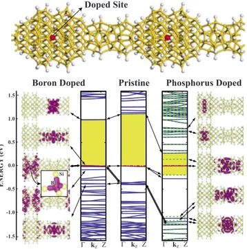
Next we examine the effect of doping of the Si157H64 superlattice by substitutional B and P impurities. Both struc-tures have odd number of electrons and hence spin-polarized calculations have been carried out. Nevertheless, B-doped structure resulted in a nonmagnetic state with half-filled band edge. P-doped structure resulted in a magnetic state with a magnetic moment of 1B. In Fig.5the electronic structure of pristine and doped superlattices are shown to follow the ef-fect of the doping on the states at the band edges. Owing to the small diameter of the superlattice, the band structure is affected by the impurity. Since the band gap of the wide part is larger than that of the narrow part, the state associated with the impurity, which occurs normally either near the valence or conduction band, falls in the bands of the narrow part.
It is known that substitutional B doping of bulk silicon crystal results in an acceptor state ⬃45 meV above the valence-band edge.22 In the substitutional doping of the su-perlattice by B similar situation occurs and the acceptor state is located above the valence-band edge corresponding to the wide part, but falls in the valence band of the narrow part. The filled first and the lower lying three valence bands at about ⬃−0.4 eV undergo changes: the filled first valance band having states confined in the narrow part becomes half filled. Three lower lying valence bands of the pristine super-lattice are raised toward the edge of the valence-band edge. The states of these bands mix with the tetrahedrally coordi-nated sp3-hybridized orbitals of B and form a triply degen-erate state just below the half-filled valence-band edge. Charge-density isosurfaces of these states around boron atom presented in Fig.5 clearly indicates sp3 hybridization in tet-rahedral directions. As a result, the “holelike states” becomes confined in the narrow part. As for the conduction band is slightly shifted down but its states preserve their character.
In P doping of the superlattice at the center of the wide part, the impurity state localized at P atom occurs in the conduction band of the superlattice. This state, in fact, is the donor state occurring ⬃200 meV below the conduction
−1 −0.5 0 0.5 1 −1 −0.5 0 0.5 1 y (A) y (A) oo −1 −0.5 0 0.5 1 −1 −0.5 0 0.5 1 x (A)o x (A)o
b)
c)
d)
e)
20 30 40 50 E(T) -E(0) (eV) Time (ps) 0 2 4 6 8 10a)
500K 1300KFIG. 4. 共Color online兲 共a兲 Energy per unit cell of Si157H64 su-perlattice as its temperature is increased from 500 to 1400 K共green/ light兲 and kept constant at 1300 K 共red/dark兲. Trajectories of atoms at the surface of共b兲 wide and 共c兲 narrow parts and at the center of 共d兲 wide and 共e兲 narrow parts of the superlattice, projected on a plane perpendicular to the wire axis, as the system is kept at 1300 K. Doped Site 1.5 0.5 0.0 1.0 -0.5 ENER G Y (eV ) -1.5 -1.0
Pristine Phosphorus Doped Boron Doped
Γ kz Z Γ kz Z Γ kz Z
B Si
FIG. 5. 共Color online兲 Atomic and electronic structure and charge-density isosurfaces of Si157H64 substitutional doped by B and P atoms关namely, Si156P共B兲H64兴. Top panel presents a view of the superlattice structure, where the doped site is represented by large red 共dark兲 ball. Arrows between the bands of the undoped 共pristine兲 superlattice and the bands of the B- and P-doped super-lattices indicate the states, which preserved their character even after doping. The charge-density isosurfaces of specific states are linked to the corresponding bands by arrows. Fermi level, repre-sented by dashed-dotted共red兲 line, was shifted to the valence-band edge and set to zero. Solid共blue兲 and dashed 共green兲 lines represent the majority- and minority-spin states, respectively. Small panel at the left-hand side presents the charge-density isosurface plot of B-Si bonds.
band corresponding to the wide part. This energy is in good agreement with the energy calculated recently for the ioniza-tion energy of P donor states in the Si nanowires.23 Below this donor state, all conduction-band states are confined ei-ther in the narrow part or at the interface but not in the wide part. Energy shifts of the band-edge states are more pro-nounced in structure having substitutional P doping. Conduction-band edge is shifted down by 0.75 eV but the charge-density profile remains the same. One spin-up and one spin-down bands split by⬃0.2 eV are formed near the conduction-band edge with charge densities localized in the narrow part. The triply degenerate state in the valance band near the edge are shifted down. That states localized around substitutional P impurity appear in the conduction-band con-tinua, while a filled spin-up band states are localized in the defect-free narrow part, indicate the possibility of modula-tion doping. In closing this secmodula-tion we note that the elec-tronic structure associated with the doping of the small di-ameter superlattices is complex and has aspects different from that in the doping of bulk Si. The small size and dimen-sionality of the doped superlattices hinders the application of the effective-mass approximation leading to hydrogenic im-purity model. For the same reason, the relative positions of band edges can be affected by the presence of a substitu-tional impurity.
III. CONCLUSION
In conclusion, we considered two specific superlattices grown in different crystallographic directions as a proof of concept. Each superlattice can be viewed to form the peri-odically repeating junctions of two hydrogen-saturated sili-con nanowires of different diameters. Since the band gaps of the constituent Si nanowires are different, the band gaps of these superlattices are modulated in real space. As a result, one-dimensional multiple quantum-well structures with
states confined in different 共wide or narrow兲 parts are formed. At strong confinement or localization, the superlat-tice structures can be viewed as a series of quantum dots. We believe that the band-gap modulation and resulting quantum-well structure and confinement can occur as long as the band-gap differences are maintained between adjacent region at both sides of the junction. Furthermore, we showed that the electronic structure resulting from the substitutional dop-ing of the superlattice is interestdop-ing and gives rise to modu-lation doping. We finally note that, the band gaps of SiNWs at both sides of junction forming the superlattice structure are underestimated by DFT/generalized gradient approxima-tion 共GGA兲 calculations. Since the systems under study are too large, these bands cannot be improved by GW calcula-tions. Nevertheless, our work is just a proof of concept. Ac-cording to our results, if the band gaps are different in dif-ferent parts of the heterostructure, confined states can occur and modulation doping of these quantum structures can be achieved. Details of energy-band structure and location of impurity states in the gap should only be taken qualitatively. Various types of electronic devices, such as resonant tun-neling double barriers generated from these superlattices, can be arranged on a single rod, where they can be connected by the metallic segments of unsaturated Si nanowires. The char-acter of these devices can be engineered by varying their growth direction and structural parameters, such as l1, l2, D1, and D2. Even if the diameters of superlattices we treated in this study are small共⬃1 nm兲 and hence in the range where band gaps vary significantly with diameter, they are still in the range of those fabricated recently.1
ACKNOWLEDGMENTS
Part of the computations have been carried out by using UYBHM at Istanbul Technical University through a Grant No. 2-024-2007. This work is partially supported by TÜBA, Academy of Science of Turkey.
1D. D. D. Ma, C. S. Lee, F. C. K. Au, S. Y. Tong, and S. T. Lee, Science 299, 1874共2003兲.
2A. K. Singh, V. Kumar, R. Note, and Y. Kawazoe, Nano Lett. 6, 920共2006兲.
3Y. Cui, Z. Zhong, D. Wang, W. U. Wang, and C. M. Lieber, Nano Lett. 3, 149共2003兲.
4Y. Huang, X. F. Duan, and C. M. Lieber, Small 1, 142共2005兲. 5X. F. Duan, Y. Huang, R. Agarwal, and C. M. Lieber, Nature
共London兲 421, 241 共2003兲.
6Y. Cui, X. F. Duan, J. Hu, and C. M. Lieber, J. Phys. Chem. B
104, 5213共2000兲.
7M. V. Fernandez-Serra, Ch. Adessi, and X. Blase, Phys. Rev. Lett. 96, 166805共2006兲.
8E. Durgun, D. Cakir, N. Akman, and S. Ciraci, Phys. Rev. Lett.
99, 256806共2007兲; E. Durgun, N. Akman, and S. Ciraci, Phys.
Rev. B 78, 195116共2008兲.
9M. S. Gudiksen, L. J. Lauhon, J. Wang, D. C. Smith, and C. M.
Lieber, Nature共London兲 415, 617 共2002兲.
10M. T. Bjork, B. J. Ohlsson, T. Sass, A. I. Persson, C. Thelander, M. H. Magnusson, K. Deppert, L. R. Wallenberg, and L. Sam-uelson, Nano Lett. 2, 87共2002兲.
11Y. Wu, R. Fan, and P. Yang, Nano Lett. 2, 83共2002兲.
12N. Akman, E. Durgun, S. Cahangirov, and S. Ciraci, Phys. Rev. B 76, 245427共2007兲.
13W. Kohn and L. J. Sham, Phys. Rev. 140, A1133 共1965兲; P. Hohenberg and W. Kohn, Phys. Rev. 136, B864共1964兲. 14D. Vanderbilt, Phys. Rev. B 41, 7892共1990兲.
15G. Kresse and J. Hafner, Phys. Rev. B 47, 558共1993兲; G. Kresse and J. Furthmuller, ibid. 54, 11169共1996兲.
16J. P. Perdew, J. A. Chevary, S. H. Vosko, K. A. Jackson, M. R. Pederson, D. J. Singh, and C. Fiolhais, Phys. Rev. B 46, 6671 共1992兲.
17L. Esaki and L. L. Chang, Phys. Rev. Lett. 33, 495 共1974兲; Highlights in Condensed Matter Physics and Future Prospects NATO Science Forum Series B Vol. 285, edited by L. Esaki,
共Plenum, New York, 1991兲.
18X. Zhao, C. M. Wei, L. Yang, and M. Y. Chou, Phys. Rev. Lett.
92, 236805共2004兲; M. Bruno, M. Palummo, A. Marini, R.
Del-Sole, and S. Ossicini, ibid. 98, 036807 共2007兲; R. Rurali, B. Aradi, Th. Frauenheim, and A. Gali, Phys. Rev. B 76, 113303 共2007兲.
19I. Ponomareva, E. Richter, A. N. Andriotis, and Madhu Menon, Nano Lett. 7, 3424共2007兲.
20S. Ciraci and I. P. Batra, Phys. Rev. B 36, 6194 共1987兲; E. Tekman, S. Ciraci, and A. Baratoff, ibid. 42, 9221共1990兲.
21M. P. Persson, A. Lherbier, Y. Niquet, F. Triozon, and S. Roche, Nano Lett. 8, 4146共2008兲.
22Handbook of Semiconductor Silicon Technology, edited by W. C. O’Mara, R. B. Herring, and L. P. Hunt 共Noyes, New Jersey, 1990兲.
23M. Diarra, Y.-M. Niquet, C. Delerue, and G. Allan, Phys. Rev. B
75, 045301共2007兲; T.-L. Chan, M. L. Tiago, E. Kaxiras, and J.
R. Chelikowsky, Nano Lett. 8, 596 共2008兲; C. R. Leao, A. Fazzio, and A. J. R. daSilva, Nano Lett. 8, 1866共2008兲.