Free-standing ZnO–CuO composite nanowire array films and their gas sensing properties
This article has been downloaded from IOPscience. Please scroll down to see the full text article. 2011 Nanotechnology 22 325704
(http://iopscience.iop.org/0957-4484/22/32/325704)
Download details:
IP Address: 139.179.14.46
The article was downloaded on 26/11/2012 at 11:29
Please note that terms and conditions apply.
View the table of contents for this issue, or go to the journal homepage for more Home Search Collections Journals About Contact us My IOPscience
Nanotechnology 22 (2011) 325704 (7pp) doi:10.1088/0957-4484/22/32/325704
Free-standing ZnO–CuO composite
nanowire array films and their gas sensing
properties
J X Wang
1, X W Sun
1,2, Y Yang
1, K K A Kyaw
1, X Y Huang
1,
J Z Yin
1, J Wei
3and H V Demir
1,41School of Electrical and Electronic Engineering, Nanyang Technological University,
Nanyang Avenue, 639798, Singapore
2Department of Applied Physics, College of Science, Tianjin University, Tianjin 300072,
People’s Republic of China
3Singapore Institute of Manufacturing Technology (SIMTech), 71 Nanyang Drive, 638075,
Singapore
4Department of Electrical and Electronics Engineering, Department of Physics,
UNAM–Institute of Material Science and Nanotechnology, Bilkent University, Ankara 06800, Turkey
E-mail:[email protected]
Received 15 March 2011, in final form 23 June 2011 Published 19 July 2011
Online atstacks.iop.org/Nano/22/325704
Abstract
A modified hydrothermal method was developed to synthesize ZnO–CuO composite
nanostructures. A free-standing film made of ZnO–CuO nanostructures was assembled on the surface of the hydrothermal solution with a smooth surface on one side and a spherical surface on the other side. The structure, growth mechanism and the optical properties of the composite nanostructures were studied. Structural characterizations indicate that the composite
nanostructure mainly consisted of two single-crystal phases of CuO and ZnO. The sensitivity for CO gas detection was significantly improved for the composite CuO–ZnO nanostructure film. This method offers a possible route for the fabrication of free-standing nanostructure films of different functional composite oxides.
S Online supplementary data available fromstacks.iop.org/Nano/22/325704/mmedia
(Some figures in this article are in colour only in the electronic version)
1. Introduction
One-dimensional (1D) metal oxide nanostructures with various morphologies, such as nanowires [1], nanotubes [2] and nanoflower [3], have been extensively investigated during the past few years. Among them, composite nanomaterials consisting of different components along the axial or radial directions may offer a combined functionality contributed by these different components. Various methods, including thermal evaporation [4,5], chemical vapor deposition [6] and wet chemical method [7], have been developed to fabricate various types of composite nanowires such as ZnO/ZnS, CdS/ZnS, Zn/ZnO and In2O3/SnO2. However, up to now, effective strategies for reliable and mass fabrication of composite nanostructures still remain a challenge. In addition,
most of the nanostructures need to be synthesized on the substrate because it provides a platform for deposition of the catalysts or the seed layer, which is important for the growth of nanostructures. However, the usage of substrates sometimes limits their wide applications in electronic devices, especially when the substrate is non-conductive. Complicated procedures need to be carried out to form the electrical contact, for example, separating the film and transferring to other substrates [8]. Direct fabrication of the free-standing film is a viable solution to overcome these limitations.
ZnO is a traditional n-type semiconductor due to the existence of oxygen vacancies. ZnO nanostructures have attracted intense research interest due to their aesthetic morphologies and potential optical and electrical applications, such as field emitter [9], ultraviolet laser [1], biosensor [10],
Nanotechnology 22 (2011) 325704 J X Wang et al
gas sensor [11,12] and transistor [13]. On the other hand, CuO is a p-type transition-metal oxide with a narrow bandgap (Eg ∼ 1.2 eV). Their nanostructures have been extensively studied in recent years and have been considered as a promising materials in many fields such as gas sensors [14], lithium ion electrode materials [15] and field emission emitters [16]. Composite nanostructures of ZnO and CuO may form a p–n junction in a one-dimensional scale. It is expected that the nanocomposites of 1D ZnO and CuO nanomaterials exhibit novel or improved properties in different fields such as gas sensors and field emitters.
In this paper, we shall report a modified hydrothermal method for the synthesis of a composite coaxial ZnO– CuO nanostructure, which forms a free-standing film on the surface of the hydrothermal solution. The structures, growth mechanism and optical properties as well as their gas sensing properties of the composite nanostructures were studied.
2. Experimental details
The ZnO–CuO composite nanowires were fabricated by a modified hydrothermal method. The reaction solution was prepared by mixing 0.05 mol l−1ZnCl2, 0.001 mM CuCl2and a proper quantity of ammonia (weight ratio 25%) in a bottle with an autoclavable screw. The pH value of the solution was adjusted by ammonia and kept at 10. Unlike the traditional hydrothermal method using a closed vessel as the reactor, in our experiment a small hole with a diameter of about 1.5 mm was opened on the top of the autoclavable screw cap. The solution was slowly heated up to 95◦C with a rate of about 1–2◦C min−1, then the temperature was kept constant for 8 h. Finally, a free-standing black film was found floating on the surface of the solution. The area of the film can reach several square centimeters. Subsequently, the as-prepared film was washed repeatedly with the deionized water and dried at 90◦C for 1 h. Then the structure and the morphologies of the film were characterized using scanning electron microscopy (SEM, JEOL JSM-5910), x-ray diffraction (XRD, Siemens D5005) and high-resolution transmission electron microscopy (HRTEM, JEOL TEM-2010F). The optical properties of the composite film were investigated using room temperature (RT) Raman spectroscopy and RT photoluminescence (PL). The gas sensing properties of the ZnO–CuO composite were characterized using a computer-controlled gas-sensing characterization system. The testing gas was diluted CO in dry air with a total flow rate of 500 sccm. The gas sensitivity S was determined by the relative resistance, S = Rair/Rgas, where Rairand Rgasare the resistance of the ZnO–CuO composite gas sensor in dry air and in dry air with CO gas, respectively.
3. Results and discussion
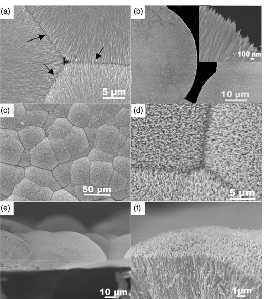
Typical SEM images of the composite film are shown in figure1. Figure1(a) shows a top-view SEM image taken on the central region of the composite ZnO–CuO film. The image indicates that the composite film is assembled by many like structures made of dense nanowires. The size of the grain-like structure can reach up to several tens of micrometers. Clear
interfaces between the hierarchical structures are observed, as indicated by the arrows in figure1(a). Interestingly, for each hierarchical structure, we observed that most of the nanowires grew horizontally but towards different orientations, forming a nanostructure film with a flat surface. Figure1(b) presents the SEM image taken on the edge of the nanostructured film. Without the confinement of other grains, the edge of the nanowire film grows in an arc-like shape. A high magnification SEM image shown in the inset of figure1(b) shows that the nanowires assembled at the edge of the film have a diameter of about 100 nm and the lengths ranged from several hundred nanometers to several micrometers. Due to the free-standing feature of the nanowire film, it is easy to be manipulated by tweezers and thus we can investigate the morphology of the nanowire film on the other side. Figures 1(c) and (d) presents the top-view SEM image of the nanowire film on the other side. Although from the images, we can also find many boundaries in between the grains, the morphology of the film is quite different. Unlike the flat surface shown in figure1(a), the surface of the grains on this side is developed to a spherical shape. The surface of the composite film looks like the assembling of many partial spherical crowns, which makes the surface of the film quite rough. The nanowires grew on the surface have the diameter of about 100 nm, which is the same as the nanowires grown on the flat side. The cross-sectional SEM images shown in figures1(e) and (f) give us a clear view of the composite nanowire film. As can be seen from the images, we can observe that the film consists of many spherical hierarchical structures, and the nanowires grow radially and perpendicularly to the spherical face.
The XRD pattern of the nanowire film is shown in figure2, where most of the diffraction peaks can be indexed to the hexagonal wurtzite phase of ZnO with lattice constants of a = 0.325 nm and c = 0.520 nm (JCPDS 80-0074). The left diffraction peaks, as indicated in the figure, are indexed to those of the monoclinic phase of CuO (JCPDS 80-1916). No other composite phase was found, which indicates the nanowire film is consisted of two different phases of ZnO and CuO.
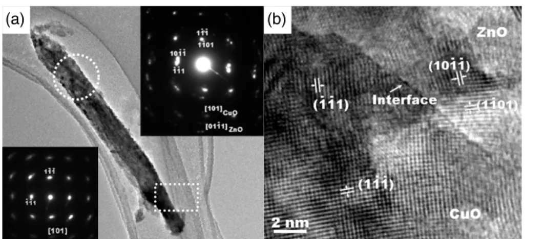
Figure 3(a) shows the bright-field TEM image of a nanowire with a diameter of about 50 nm. From the TEM image, we can observe that the nanowire shows a thin tip with different contrast (marked by squares). The corresponding SAED taken from the tip is shown in the bottom-left inset of figure 3(a). Regular and bright spots of the SAED indicate the single-crystalline feature of the nanowire. The SAED is indexed to be monoclinic phase CuO taken along the [¯101] zone axis. The growth direction of the nanowire can also be determined to be the [020] direction of CuO. However, the SAED taken from the center of the nanowire shows a different pattern (circle region), as shown in the top-right inset of figure3(a). The SAED pattern indicates two sets of diffraction spots. One can be indexed to be a hexagonal ZnO pattern along the [01¯11] zone axis. Another set of SAED patterns belongs to monoclinic CuO along the [¯101] zone axis, which is the same as the SAED pattern taken from the tip of the nanowire. The SAED results clearly demonstrate that the nanowire consisted of two different phases of ZnO and CuO. Figure3(b) shows an 2
(a) (b)
(c) (d)
(e) (f)
Figure 1. Top-view SEM images of (a) composite ZnO–CuO film taken on the central region and (b) edge of the composite film. Inset is the enlarged SEM image taken on the edge of the composite film (c). (d) Top-view SEM image of the composite film on another side.
(e) Cross-sectional SEM image of composite film. (f) Enlarged cross-sectional SEM image of composite film.
HRTEM image taken from the edge of the nanowire. A clear interface between two phases can be observed with different contrasts. At the region above the interface, two groups of parallel fringes with a d spacing of 0.25 and 0.23 nm can be indexed, which correspond to the (¯11¯1) and (111) planes of monoclinic CuO, respectively. In addition, at the edge of the nanowires, another two groups of the parallel fringes can be indexed to the (1¯101) and (¯1011) planes of wurtzite ZnO, respectively. The TEM and HRTEM results demonstrated that the nanowire is a composite structure with two separate phases CuO and ZnO, respectively.
It is worth mentioning that no composite nanostructures were found on the silicon substrate placed on the bottom of the solution. Instead, ZnO nanorod arrays with uniform diameters and lengths were observed (see supporting information, figure S1 available atstacks.iop.org/Nano/22/325704/mmedia). TEM analysis indicated that all the growth direction of the ZnO nanorods is in the [0001] direction (see supporting information, figure S1 available at stacks.iop.org/Nano/22/ 325704/mmedia), which is different from the direction of the ZnO shell coated on the CuO surface. Obviously, the growth
Figure 2. XRD pattern of the composite ZnO–CuO nanostructure film.
orientation of the ZnO was confined by the CuO phase. As we know, composite structures can form easily when the planes of the two different materials have close inter-plane
Nanotechnology 22 (2011) 325704 J X Wang et al
(a) (b)
Figure 3. (a) Bright-field TEM image of a nanowire. The insets are SAED patterns taken from the tip (bottom left) and the center (top right) of the nanowire. (b) HRTEM image of the composite ZnO–CuO nanowires.
spacing and similar crystal orientations as well as similar crystal structures. The similar phenomenon was also observed in the ZnO–SnO2 composite system [17]. In this work, CuO has a monoclinic structure while ZnO has a hexagonal wurtzite structure. However, the CuO{111} and ZnO{¯1011} planes have an inter-plane spacing of 0.252 nm and 0.247 nm, respectively. The angle between the CuO (111) and (¯11¯1) planes is 84◦, which is close to the included angle between the ZnO (¯1011) and (10¯1¯1) (calculated to be 80◦). The mismatch between these crystal planes are relatively small and thus of benefit to form the composite CuO–ZnO structure.
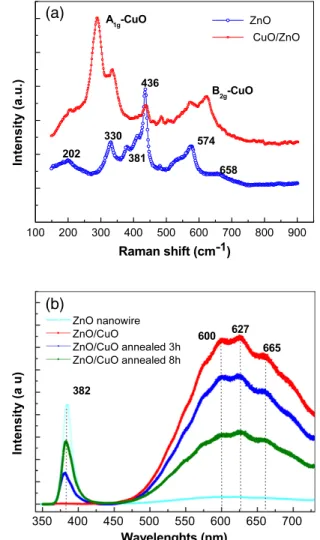
Figure4(a) shows the room temperature Raman spectrum of the ZnO–CuO core shell structures. As a reference, the Raman spectrum of pure ZnO nanowire arrays grown at the same condition is also presented. As we know, wurtzite ZnO belongs to the space group of C6v, with six active Raman modes of E2L+ E2H+ A1T+ A1L+ E1T+ E1L[18,19]. The Raman spectrum of the pure ZnO nanowire arrays exhibited six peaks at 202, 330, 380, 436, 574 and 658 cm−1. Among these peaks, the three peaks at 380, 436 and 576 cm−1 are assigned to A1T, E2H and A1Lmodes, respectively, while the peaks at 202, 380 and 658 cm−1 emerged due to the multi-phonon processes. The three peaks were assigned to 2E2L,
[E2L− E2H] and [E2L+ B1H] modes, respectively. Compared to pure ZnO nanowires, the Raman spectrum of the ZnO– CuO composite structure shows two additional peaks at 286 and 627 cm−1. These two peaks correspond to the A1g and B2g modes of crystalline CuO due to the vibrations of the oxygen atoms. However, compared to the literature [20], a redshift of the Raman peaks is observed. This may be due to the introduction of the stress during the growth process of the composite nanostructures. The coexistence of the CuO and ZnO Raman modes in the Raman spectra further confirms that the structure is a composite nanostructure, consistent with the XRD and TEM results.
Figure 4(b) shows the room temperature PL spectrum of the ZnO–CuO composite nanowires as well as the pure ZnO nanowires excited by a 325 nm He–Cd laser. As we can see from the spectra, the PL of the pure ZnO nanowires shows a sharp peak centered at 382 nm and a very weak broad band ranging from the green to the red region. The
UV peak at 382 nm is ascribed to the near-band-edge exciton recombination [21]. Compared to the PL of the ZnO nanowire, the PL of the as-prepared ZnO–CuO composite nanowires only shows a broad band with three shoulder peaks at 600, 627 and 665 nm, respectively. This broad band is attributed to the luminescence of the native or dopant-induced defects in ZnO–CuO nanowires [22]. It is worth noticing that the three shoulder peaks at 600, 628 and 665 nm can be ascribed to the PL of the ZnO phase, which have been observed in ZnO nanowires and films [23–25]. The peaks at 600 and 628 nm may be caused by the monovalent vacancies of zinc(V+Zn) and
(Vo−), while the red peak at 665 nm is attributed to the single-and double-ionized oxygen vacancies. No PL-peak-related CuO phase were observed. Therefore, the PL is originated from the luminescence of the ZnO grown on the surface of the CuO nanowires. Usually, Cu doping in ZnO usually leads to the green emission [26,27]. However, in our case, the green emission was not obvious, which may indicate Cu doping may not be significant in our ZnO–CuO composite nanostructure. The PL of the ZnO–CuO composite nanowires annealed in oxygen at 500◦C for 3 and 8 h are also shown in figure4(b). After annealing, the UV peak at 382 nm was observed and the intensity of the peaks increases while the intensity of the broad band reduces with the increase in annealing time. This may be due to the reduction of the crystal defects in the ZnO layer during the annealing process.
According to the above experimental observation, we investigated the growth mechanism of the ZnO–CuO composite nanowire film. As we know, metal ions such as Cu2+ and Zn2+ can react with the excess NH3·H2O to form amino complexes easily. When the amino complexes were heated, they decomposed to CuO and ZnO, respectively. The following reactions should take place in the aqueous solutions: Cu2++ NH3·H2O←→ Cu(NH3)24+ + OH−←→ CuO + NH 3+ H2O (1) Zn2++ NH3·H2O←→ Zn(NH3)24+ + OH−←→ ZnO + NH 3+ H2O. (2)
For the formation of composite ZnO–CuO nanostructures, CuO nanowires will form first at an early stage before the 4
(a)
(b)
Figure 4. (a) Raman spectrum of composite ZnO–CuO nanostructure film and pure ZnO nanowire array. (b) Room
temperature PL spectrum of the ZnO–CuO composite nanowires and pure ZnO nanowire array.
precipitation of the ZnO phase. This assumption is supported by our experiment results; we found that the CuO can be easily precipitated from solution below 75◦C. However, at this temperature, ZnO cannot be formed. Therefore, when the solution was slowly heated up to 95◦C, the CuO phase will first be precipitated. Due to the small concentration of Cu2+in the reactant, the Cu2+in solution vanished after the precipitation of the CuO. When the temperature keeps rising and reaches the critical value for ZnO precipitation, ZnO will precipitate on the surface of the CuO nanowires forming composite ZnO–CuO structures.
We found the small hole on the screw cap played an important role in the formation of the free-standing films. In our experiment, no films can be formed on the solution without the hole in the screw. Owing to the existence of the small hole, NH3 and water can escape slowly from the hole when the solution is heated up. The reduction of NH3 and H2O will move the reactions (1) and (2) to the right and thus facilitate the precipitation of the oxides. Most importantly, the evaporation of the NH3 and H2O will first occur in a thin layer on the solution–air interface. Therefore, in this region, NH3 and H2O will escape first: as a result, reactions
Figure 5. Schematic illustrations of the growth process of the composite ZnO–CuO nanostructure film.
take place first at the surface of the solution, which was supported by the fact that the free-standing film formed only on the surface of the solution. A schematic model shown in figure5is used to illustrate the synthesis process of the free-standing film. First, the composite nanostructures nucleated on the surface of the solution and then grew radially towards the solution because the reactants can only come from the solution. Subsequently, the composite nanostructure developed into hierarchical spherical structures floating on the surface of the solution due to the surface tension. With further growth of the hierarchical structures, the hierarchical structures connect to each other, forming a free-standing film. Because of the confinement of the solution surface, the nanowires can only grow horizontally at the surface plane and thus finally form a flat surface on one side of the composite film.
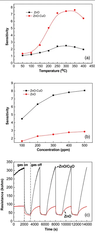
ZnO is a traditional sensing material for the detection of toxic and flammable gases. However, compared to other gases such as H2and NH3, ZnO is less sensitive for the detection of CO gas because the detection of gases is mainly based on the catalytic oxidation of gas molecules on n-type semiconductor surfaces, where H2 can be oxidized more easily than CO. The bulk heterocontact ZnO–CuO composite materials have been demonstrated to improve the sensitivity as well as the reproducibility of the CO gas sensor since the introduction of the p-type CuO forms a heterocontact interface with the ZnO [28–33]. Yanagida et al suggested that the adsorbed CO molecules form interface states that can change the potential barrier height and consequently the current across the junction [31]. In our case, the nanowires consisting of CuO and ZnO phases form the heterocontact interface on the nanoscale. The CO gas sensing properties of the composite ZnO–CuO are expected to be improved. Therefore, a gas sensor based on the composite nanostructure film was fabricated. Because of the free-standing feature, the gas sensor is simply constructed by directly attaching two gold pads on the surface of the composite films. The ZnO–CuO gas sensor was then exposed to CO gas in ambient air. As a reference, a gas sensor based on a pure ZnO nanowire array was also fabricated and measured. Since the sensor presented different responses at various testing temperatures and concentrations of the testing gas, we first investigated the effect of these two factors. Figures6(a) and (b) plot the sensitivity of the ZnO–CuO and ZnO gas sensors as a function of temperature and concentration of CO gas,
Nanotechnology 22 (2011) 325704 J X Wang et al
(a)
(b)
(c)
Figure 6. The sensitivity of the ZnO–CuO composite nanostructure and ZnO nanorod gas sensor as a function of (a) temperature and (b) concentration of CO gas. (c) Sensing responses of the gas sensor based on ZnO–CuO composite nanostructures and the ZnO nanowire exposed to 300 ppm CO gas at temperature 300◦C.
respectively. As can be seen from figure6(a), the sensitivity of both ZnO–CuO and ZnO sensors reaches the maximum in the temperature range from 250 to 350◦C. Therefore, 300◦C was chosen as the testing temperature to measure the sensing properties of the ZnO–CuO sensors. In addition, the calibration curves shown in figure6(b) indicate that the ZnO– CuO microtube sensor shows an increasing response following the increase of the gas concentration but it increases slowly for
higher CO concentrations over 400 ppm. Figure6(c) shows the sensing responses of the corresponding ZnO–CuO composite nanostructure and the ZnO nanowire gas sensors when exposed to 300 ppm CO gas at 300◦C. At this temperature, the ZnO– CuO composite shows higher resistance at the initial stage than the ZnO nanowire, which is due to the high resistance of the CuO phase in the composite. In figure6, we found that both the resistance of the composite ZnO–CuO and ZnO sensors reduces in the presence of 300 ppm CO. The reversible cycles of the response curve of the composite ZnO–CuO gas sensor indicate a stable and repeatable operation, with a sensitivity S of about 7.6. Although the ZnO nanowire gas sensor also shows a reversible response to CO gas at the same temperature, the sensitivity of the composite ZnO–CuO sensor is obviously higher than that of the pure ZnO nanowire. The sensitivity of composite ZnO–CuO nanostructures is over three times that of ZnO nanowires, indicating the improved sensitivity of the ZnO–CuO composite to the CO gas. Moreover, we also found that both the response and recovery times of the composite ZnO–CuO gas sensor are faster than those of the ZnO nanowire sensor. For a composite ZnO–CuO sensor, the response and recovery times are 26 s and 1048 s, respectively, while for the ZnO nanowire sensor, the response and recovery times are 238 s and 1354 s, respectively. The response time is remarkably improved for the ZnO–CuO sensor. These results indicate that better performance can be achieved with a composite ZnO–CuO nanostructure film sensor compared to a single-phase nanowire ZnO gas sensor. We also noted that in figure 6(c) a slight resistance drift occurred, which may due to the inhomogeneous morphologies of the ZnO– CuO composite nanostructures. The free-standing composite films synthesized by the hydrothermal method consist of many spherical crowns and thus form a rough surface. We optimize the growth condition to get the uniform composite film which may help to further improve the stability of the composite ZnO–CuO sensor. This will be our future research direction towards the better performance of the ZnO–CuO sensor.
4. Conclusion
In summary, we have presented a hydrothermal method for the synthesis of free-standing composite ZnO–CuO films on the surface of the hydrothermal solution by controlling the chemical reaction dynamics. The film is made of the assembled composite CuO/ZnO nanostructures and possesses a flat surface on one side and a rough surface on the other side. The formation of the composite CuO/ZnO nanostructure undergoes a two-step process in which the ZnO layer grew on the surface of the CuO nanowires. The composite CuO/ZnO nanostructures showed remarkably improved sensing properties for CO gas compared to the single-phase ZnO nanowires. This method may also be applied in other composite systems to synthesize many other functional composite oxide nanostructures.
References
[1] Huang M H, Mao S, Feick H, Yan H Q, Wu Y Y, Kind H, Weber E, Russo R and Yang P D 2001 Science292 1897 6
[2] Martinson A B F, Elam J W, Hupp J T and Pellin M J 2007
Nano Lett.7 2183
[3] Jiang C Y, Sun X W, Lo G Q, Kwong D L and Wang J X 2007
Appl. Phys. Lett.90 263501
[4] Wang J X, Xie S S and Zhou W 2007 MRS Bull.32 123
[5] Zeng H, Li Z, Cai W, Cao B, Liu P and Yang S 2007 J. Phys.
Chem. B111 14311
[6] Hsu Y J and Lu S Y 2004 Chem. Commun.2102 [7] Du N, Zhang H, Chen B D, Wu J B and Yang D R 2007
Nanotechnology18 115619
[8] Wong W S, Sands T and Cheung N W 1998 Appl. Phys. Lett.
72 599
[9] Zhu Y W, Zhang H Z, Sun X C, Feng S Q, Xu J, Zhao Q, Xiang B, Wang R M and Yu D P 2003 Appl. Phys. Lett.
83 144
[10] Wang J X, Sun X W, Wei A, Lei Y, Cai X P, Li C M and Dong Z L 2006 Appl. Phys. Lett.88 233106
[11] Wang J X, Sun X W, Huang H, Lee Y C, Tan O K, Yu M B, Lo G Q and Kwong D L 2007 Appl. Phys. A88 611
[12] Wang J X, Sun X W, Yang Y and Wu C M L 2009
Nanotechnology20 465501
[13] Fan Z Y, Wang D W, Chang P C, Tseng W Y and Lu J G 2004
Appl. Phys. Lett.85 5923
[14] Kim Y S, Hwang I S, Kim S J, Lee C Y and Lee J H 2008
Sensors Actuators B135 298
[15] Gao S Y, Yang S X, Shu J, Zhang S X, Li Z D and Jiang K 2008 J. Phys. Chem. C112 19324
[16] Zhu Y W, Yu T, Cheong F C, Xui X J, Lim C T, Tan V B C, Thong J T L and Sow C H 2005 Nanotechnology16 88
[17] Wang J X, Sun X W, Xie S S, Yang Y, Chen H Y, Lo G Q and Kwong D L 2007 J. Phys. Chem. C111 7671
[18] Bundesmann C, Ashkenov N, Schubert M, Spemann D, Butz T, Kaidashev E M, Lorenz M and Grundmann M 2003 Appl.
Phys. Lett.83 1974
[19] Manj´on F J, Mar´ı B, Serrano J and Romero A H 2005 J. Appl.
Phys.97 053516
[20] Yu T, Zhao X, Shen Z X, Wu Y H and Su W H 2004 J. Cryst.
Growth268 590
[21] Hu J Q and Bando Y 2003 Appl. Phys. Lett.82 1401
[22] Zhu Y W, Sow C H, Yu T, Zhao Q, Li P H, Shen Z X, Yu D P and Thong J T L 2006 Adv. Funct. Mater.16 2415
[23] Lin B X, Fu Z X and Jia Y B 2001 Appl. Phys. Lett.79 943
[24] Jin B J, Im S and Lee S Y 2000 Thin Solid Films366 107
[25] Park W I, Jun Y H, Jung S W and Yi G C 2003 Appl. Phys.
Lett.82 964
[26] Zhou S M, Zhang X H, Meng X M, Zou K, Fan X, Wu S K and Lee S T 2004 Nanotechnology15 1152
[27] Garces N Y, Wang L, Bai L, Giles N C, Halliburton L E and Cantwell G 2002 Appl. Phys. Lett.81 622
[28] Bae H Y and Choi G M 1999 Sensors Actuators B55 47
[29] Choi J D and Choi G M 2000 Sensors Actuators B69 120
[30] Jun S T and Choi G M 1994 Sensors Actuators B17 175
[31] Nakamura Y, Ando A, Tsurutani T, Okada O, Miyayama M, Koumoto K and Yanagida H 1986 Chem. Lett.3 413
[32] Nakamura Y, Yoshioka H, Miyayama M, Yanagida H, Tsurutani T and Nakamura Y 1990 J. Electrochem. Soc.
137 940
[33] Nakamura Y, Zhuang H X, Kishimoto A, Okada O and Yanagida H 1998 J. Electrochem. Soc.145 632