Miniaturized negative permeability materials
Kamil Boratay Alici, Filiberto Bilotti, Lucio Vegni, and Ekmel Ozbay
Citation: Appl. Phys. Lett. 91, 071121 (2007); doi: 10.1063/1.2772672 View online: http://dx.doi.org/10.1063/1.2772672
View Table of Contents: http://aip.scitation.org/toc/apl/91/7 Published by the American Institute of Physics
Miniaturized negative permeability materials
Kamil Boratay Alicia兲Nanotechnology Research Center, Bilkent University, 06800 Ankara, Turkey and Department of Physics, Bilkent University, 06800 Ankara, Turkey
Filiberto Bilotti and Lucio Vegni
Department of Applied Electronics, University of Roma Tre Via della Vasca Navale, 84-00146, Rome, Italy
Ekmel Ozbay
Nanotechnology Research Center, Bilkent University, 06800 Ankara, Turkey; Department of Physics, Bilkent University, 06800 Ankara, Turkey; and Department of Electrical and Electronics Engineering, Bilkent University, 06800 Ankara, Turkey
共Received 30 May 2007; accepted 26 July 2007; published online 17 August 2007兲
Experimental and numerical studies of -negative 共MNG兲 materials such as multisplit ring resonators 共MSRRs兲 and spiral resonators 共SRs兲 are presented. The resonance frequency of the structures is determined by the transmission measurements and minimum electrical size of0/ 17 for
the MSRRs and of0/ 82 for the SRs observed. These MNG materials can be easily produced by the
well developed printed circuit board and optical lithography techniques. They are promising elements for the development of high resolution metamaterial lenses and electrically small antennas. © 2007 American Institute of Physics.关DOI:10.1063/1.2772672兴
Electromagnetic metamaterials possess unusual proper-ties, such as the reversal of both Cherenkov radiation and Doppler shift, as well as a negative index of refraction,1 which enables subwavelength imaging.2 Experimental dem-onstration of negative refraction is conducted by using a composite medium.3 The elements of the medium are thin wires and split ring resonators. The periodic arrangement of the thin wires provides a negative effective permittivity at the frequencies lower than the plasma frequency of the system.4The split ring resonator is an example of magnetic microstructures that are designed to generate a negative ef-fective permeability.5The study of-negative共MNG兲 struc-tures is of considerable interest due to the various imaging and antenna applications.
In magnetic resonance imaging, the introduction of MNG materials improved image quality by guiding the radio frequency flux from an object to a receiver.6 The subwave-length image of the second-harmonic field of a source can be obtained by using a metamaterial slab with a quadratic non-linear response.7Moreover, by using a one-dimensional left-handed metamaterial, subwavelength imaging at microwave frequencies is demonstrated experimentally.8Loading anten-nas with MNG materials can improve their performance, es-pecially in terms of achieving smaller sizes. MNG material loaded monopole antenna,9 patch antenna,10–12 and waveguides13,14 are studied in the literature. In all of these applications, the rather small electrical size of the structures is favorable.
The miniaturization of MNG materials is realized by changing the geometry of the structures. The most common MNG material is the split ring resonator. There are two flat disks, each of which are made discontinuous with a split, and which are separated from each other by a gap.5Instead of flat disks, long cylindrical sheets can also be used.5,15In order to increase the distributed capacitance, cylindrical sheets are wound as coils, in which the structure is called a Swiss roll.5,6The flat version of the Swiss roll is called the spiral
resonator,10,16which is commonly used as a lumped inductor in microwave engineering.17 In addition to changing the ge-ometry of the structures, one can introduce lumped elements to the existing structures. A capacitance loaded loop,18ring,19 double sided spiral,20and split ring resonators21can be found in the literature.
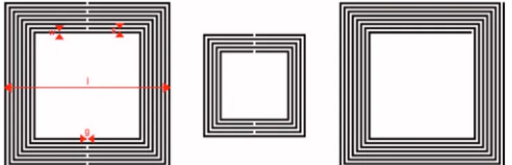
However, in most of the above examples, fabrication is a difficult and tedious procedure. The arrays of Swiss rolls, long cylindrical sheets, and capacitively loaded elements cannot be produced easily. Moreover, the Swiss rolls and long cylindrical sheet structures are strongly anisotropic, and due to the purely electrical effects at the axis of the cylinders, they respond as an effective metal when the incident wave polarization is at the axis of the cylinders. On the other hand, the structures, which are considerably thin at the axis of cyl-inders, can be packed into arrays in three dimensions. By this technique an isotropic medium can be obtained in principle.5 In the present work, we study electrically small MNG materials that can be produced relatively easily in the domain of well developed printed circuit board manufacturing tech-niques and optical lithography processes. The structures are multisplit ring resonators 共MSRRs兲 and a version of spiral resonators 共SRs兲. The MSRR consists of concentric split rings that are designed in order to increase the distributed capacitance between the strips关Fig. 1共a兲兴. The geometrical parameters of the structure are as follows: the side length of the outer ring l = 8 mm, the strip width w = 100m, the
sepa-a兲Electronic mail: [email protected]
FIG. 1. 共Color online兲 Geometry of examples of MNG materials: 共a兲 Mul-tisplit ring resonator with side length l = 8 mm and number of rings N = 8;共b兲 multisplit ring resonator with l = 5, N = 5;共c兲 spiral resonator with l=8 mm and number of turns N = 8.
APPLIED PHYSICS LETTERS 91, 071121共2007兲
ration between adjacent strips s = 100m, and the split width
g = 100m. One other example of the MSRRs is shown in Fig.1共b兲, in which all of the parameters are the same, ex-cepting the side length of the outer ring共l=5 mm兲. In Fig. 1共c兲 the SR geometry is shown, in which we also have
s = w = 100m and l = 8 mm. A parameter of considerable in-terest for the MSRRs共SRs兲 is N: number of strips 共number of turns兲. We kept the dimensions of the structures fixed while changing the number of strips.
These MNG materials are fabricated on a RT/duroid 5880 substrate with listed relative permittivity =2.0 and dissipation factor tan␦= 0.0009 at 10 GHz. The thickness of the printed circuit board共PCB兲 was 254m and the depos-ited copper thickness on the board was 18m. The MNG materials were obtained by properly etching the metal de-posit of the PCB.
At this point, it is necessary to identify a standard for the determination of the size of the MNG materials. We follow a rather fundamental paper that discusses the theoretical limits of the antennas.22 While defining the electrical size of a structure, we consider the minimum sphere that can enclose it. If the radius of the sphere is a, then the larger linear dimension of the structure is 2a. The electrical size共2a兲 is identified in terms of the free space wavelength共0兲 at which
the structure operates: u = 2a /0. The calculated minimum
radius共a兲 and electrical size 共u兲 of the miniaturized MNG materials in the literature are shown in TableI.
In the present work, the resonance frequencies of the MNG materials are calculated numerically by using the com-mercial software CST MICROWAVE STUDIO. This tool is a three-dimensional full-wave solver employing the finite inte-gration technique.23 We excite a layer of MNG materials with a plane wave and obtain the transmission amplitudes. The dip of the transmission data gives an estimate of the resonance frequency of the structure. The structure shows the MNG behavior after the resonance frequency.
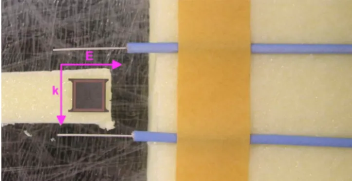
The resonant response of an single MNG material is measured by using two coaxial probes connected to an HP8510C network analyzer. First, we measure the transmis-sion spectra of the free space, i.e., without the MNG mate-rial. We use these data for calibration and then repeat the experiment with the MNG material inserted 共Fig. 2兲. The positive transmission values in Fig.3are due to the calibra-tion technique and the lensing effect of the structures. The distance between the receiver and transmitter probes is kept fixed during the measurements.
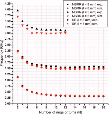
The experimental and numerical results are shown in Figs.3 and4. For the MSRR and SR materials, as we in-crease the number of rings or number of turns, the resonance frequency shifts toward smaller values. The miniaturization factor for the SRs is higher than the MSRRs. In Fig.4, we see that increasing the number N above a critical point does
not reduce the resonance frequency anymore. The resonance frequency of the MSRR can be significantly reduced up to 4–5 rings 共N=5兲. From Fig. 4 we conclude that it is not necessary to completely fill the inner part of the SR in order to obtain a good reduction of the resonance frequency. Simi-lar to the case of the MSRR, we see that after some point, increasing the number N does not affect the resonance fre-quency. The calculated electrical size共u兲, radius of the mini-mum sphere共a兲, and resonance frequency 共f0兲 for the
opti-mum structures are shown in Table I. The reduction of the resonance frequency is comparable with the examples found in the literature. The MNG materials are relatively easy to fabricate, low profile, and thereby can be packed into arrays in several dimensions. For the two MSRR examples, we see that increasing the number of rings can reduce the electrical size. This principle is also valid for the SRs. Moreover, using a higher permittivity substrate will lead us to the further reduction of the resonance frequency. These results can be explained by the aid of theoretical analysis and modeling of the SRs in literature.24,25 Moreover, a detailed analysis and circuit model of our structures is given in Ref.26.
The incident electromagnetic wave induces current on the resonators. At the resonance frequency, the electric and magnetic energy in the structure increases dramatically. Since the structures are small compared to the wavelength, the results can be explained by a quasistatic approach. We consider the change of the total inductance 共L兲 and capaci-tance共C兲 of the structures as the number of rings or turns increases. The significant parameters to determine the L and
C are the average length of the strips and their filling ratio.26
There are three important results to be explained: the de-crease of the resonance frequency, miniaturization factor dif-ference between the MSRR and SR structures, and the satu-ration behavior.
As N gets larger values the capacitance of the structures increases while the inductance decreases. Since the propor-tion decrease of the inductance is smaller than the proporpropor-tion
TABLE I. Comparison of the MNG materials in the literature in terms of electrical size共u兲, resonance frequency 共f0兲, and radius of the minimum sphere 共a兲.
The free space wavelength is denoted as0.共Capacitance loaded is abbreviated as C.L.兲 The exact numbers of rings 共turns兲 given in the last three columns
are N = 12 for the MSRR structures and N = 20 for the SR structure. Swiss roll Cylindrical SRR C.L. loop C. L. ring C.L. double sided spiral C.L. SRR MSRR 共1=8兲 MSRR 共1=5兲 SR 共1=8兲 a共mm兲 100.1 8.2 6.8 14.0 6.5 3.7 5.7 3.5 5.7 f0共MHz兲 22.1 1440.0 60.0 46.2 156.4 990.0 1545.0 3105.0 323.5 u共0兲 1 / 68 1 / 13 1 / 367 1 / 232 1 / 148 1 / 41 1 / 17 1 / 14 1 / 82
FIG. 2. 共Color online兲 Experiment setup 共photo兲. The polarization of the incident wave is also shown.
increase of the capacitance, we observe a shift of the reso-nance frequency to lower values. The proportion capacitance difference between the MSRRs and SRs is due to the split capacitance of the MSRRs. The total split capacitance of the MSRRs is significantly smaller than the distributed one. Therefore, as we change the number of rings 共turns兲, the proportion capacitance change of the MSRRs and SRs shows a similar behavior. The miniaturization factor difference of the MSRRs and SRs is related to inductance.26 For the MSRRs in addition to the average length of the strips, the filling ratio has an additional decreasing effect on the induc-tance. Therefore, the proportion decrease of the inductance is higher for the MSRRs that give a smaller miniaturization factor. The saturation of the resonance frequency is due to the saturation of both the inductance and the capacitance of the structures. The average length and the filling ratio in-crease with a decreasing rate, which yields a saturation behavior.26
In summary, we experimentally demonstrated electri-cally small MNG materials. For the MSRR structures, the electrical size of 0/ 17 and for the SR structures electrical
size of0/ 82 is achieved. Further size reduction can be
re-alized by increasing the number N or using a higher permit-tivity substrate. The MNG materials are relatively easy to fabricate, low profile, and can be packed into arrays. Since the electrical size of the metamaterial element limits the
resolution of the subwavelength imaging, the MNG materials demonstrated here can be the first step toward the metama-terial based ultrahigh resolution imaging systems. Moreover, they establish a solution for the antenna miniaturization problem in wireless systems.
This work is supported by the European Union under
the projects EU-NoE-METAMORPHOSE,
EU-NoE-PHOREMOST, and TUBITAK under Project Nos. 104E090, 105E066, 105A005, and 106A017. One of the authors共E.O.兲 also acknowledges partial support from the Turkish Academy of Sciences.
1V. G. Veselago, Sov. Phys. Usp. 10, 509共1968兲. 2J. B. Pendry, Phys. Rev. Lett. 85, 3966共2000兲.
3D. R. Smith, W. J. Padilla, D. C. Vier, S. C. Nemat-Nasser, and S. Schultz,
Phys. Rev. Lett. 84, 4184共2000兲.
4J. B. Pendry, A. J. Holden, W. J. Stewart, and I. Youngs, Phys. Rev. Lett. 76, 4773共1996兲.
5J. B. Pendry, A. J. Holden, D. J. Robbins, and W. J. Stewart, IEEE Trans.
Microwave Theory Tech. 47, 2075共1999兲.
6M. C. K. Wiltshire, J. B. Pendry, I. R. Young, D. J. Larkman, D. J.
Gilderdale, and J. V. Hajnal, Science 291, 849共2001兲.
7A. A. Zharov, N. A. Zharova, I. V. Shadrivov, and Yu. S. Kivshar, Appl.
Phys. Lett. 87, 091104共2005兲.
8A. N. Lagarkov and V. N. Kissel, Phys. Rev. Lett. 92, 077401共2004兲. 9K. B. Alici and E. Ozbay, J. Appl. Phys. 101, 083104共2007兲.
10K. Buell, H. Mosallaei, and K. Sarabandi, IEEE Trans. Microwave Theory
Tech. 54, 135共2006兲.
11A. Alù, F. Bilotti, N. Engheta, and L. Vegni, IEEE Trans. Antennas
Propag. 55, 13共2007兲.
12P. Ikonen, M. Karkkainen, and S. Tretyakov, IEEE AP-S International
Symposium, Washington DC, 3–8 July 2005共IEEE, New York, 2005兲, Vol. 2a, pp. 606–609.
13S. Hrabar, J. Bartolic, and Z. Sipus, IEEE Trans. Antennas Propag. 53,
110共2005兲.
14R. Marqués, J. Martel, F. Mesa, and F. Medina, Phys. Rev. Lett. 89,
183901共2002兲.
15M. Shamonin, E. Shamonina, V. Kalinin, and L. Solymar, Microwave Opt.
Technol. Lett. 44, 133共2005兲.
16J. D. Baena, R. Marques, F. Medina, and J. Martel, Phys. Rev. B 69,
014402共2004兲.
17I. Bahl and P. Bhartia, Microwave Solid State Circuit Design, 2nd ed.
共Wiley, New York, 2003兲, Vol. I, pp. 57–63.
18M. C. K. Wiltshire, E. Shamonina, I. R. Young, and L. Solymar, Electron.
Lett. 39, 215共2003兲.
19O. Sydoruk, A. Radkovskaya, O. Zhuromskyy, E. Shamonina, M.
Shamonin, C. J. Stevens, G. Faulkner, D. J. Edwards, and L. Solymar, Phys. Rev. B 73, 224406共2006兲.
20R. R. A. Syms, I. R. Young, and L. Solymar, J. Phys. D 39, 3945共2006兲. 21K. Aydin and E. Ozbay, J. Appl. Phys. 101, 024911共2007兲.
22L. J. Chu, J. Appl. Phys. 19, 1163共1948兲.
23User Manual, Version 5.0, CST GmbH, Darmstadt, Germany, 2005, http://
www.cst.de
24S. S. Mohan, M. Hershenson, S. P. Boyd, and T. H. Lee, IEEE J.
Solid-State Circuits 34, 1419共1999兲.
25C. R. Simovski and A. A. Sochava, Prog. Electromagn. Res. 43, 239
共2003兲.
26F. Bilotti, A. Toscano, and L. Vegni, IEEE Trans. Antennas Propag.共to be
published兲.
FIG. 3.共Color online兲 Experimental trans-mission data as a function of the fre-quency.共a兲 Multisplit ring resonators with the side length l = 8 mm. 共b兲 Multisplit ring resonators with the side length l = 5 mm. 共c兲 Spiral resonators with the side length l = 8 mm.
FIG. 4.共Color online兲 Resonance frequency as a function of the number of rings and turns共experiment and simulation兲.