т Ш WÄVE6ÜIDE
0 И Гàm ¿ W I i yr^ ¿Ü BM IÎTEÖ ГО ХІЙІЙ ІЖ'іУа/Ш ЕЬІТ OF ГГі:Г І2СЗ :0 ГГ-0 П;і-2Г'іДU'XB ОР^ВКСГМЕЕШ-Ш ÂMD SCÏEKCBS OF ВВиіЕЫТ UMirniLOSiïT ОІіОШГОіЫГ GF Ш Е к Ш О і FOR Ï H E DEGREE OF o f ЕСііШ Ш * ■ > © еKâmuran ТМоШ и
¿■■abiuSiX iSS4
RIDGE WAVEGUIDE GaAs/AUGa,_:,As
MULTIPLE QUANTUM WELL LASER DIODES
A THESIS
SUBMITTED TO THE DEPARTMENT OF PHYSICS AND THE INSTITUTE OF ENGINEERING AND SCIENCE
OF BILKENT UNIVERSITY
IN PARTIAL FULFILLMENT OF THE REQUIREMENTS FOR THE DEGREE OF
MASTER OF SCIENCE
By
Abdullah Kamuran Tiirkoglu
February, 1994
\ о ±
81
.· oo il ta..
г -
§ < 9I certify that I have read this thesis and that in my opinion it is fully adequate, in scope and in quality, as a thesis for the degree of Master of Science.
Prof. Atilla Aydınlı (Supervisor)
I certify that I have read this thesis and that in my opinion it is fully adequate, in scope and in quality, as a thesis for the degree of Master of Science.
r. Recai Ellialtioglu Assoc. Prof. Dr.
I certify that I have read this thesis and that in my opinion it is fully adequate, in scope and in quality, as a thesis for the degree of Meister of Science.
Approved for the Institute of Engineering and Science:
Prof. M ehm eL^ray,
A b stra ct
RIDGE WAVEGUIDE GaAs/AUGai_^As
MULTIPLE QUANTUM WELL LASER DIODES
Abdullah Kamuran Tiirkogiu
M. S. in Physics
Supervisor: Prof, AtiUa Aydınlı
February, 1994
The study of solid-state laser structures in low dimensions has gained great deal of attention in recent years. The theory originated in early 1960s developed really fast along with new fabrication methods bringing geometries from macroscopic to sub-micron scale. This, in turn, made it possible to realize more complex semiconductor laser structures having multiple quantum wells in their active region with sub-milliampere threshold currents and tens of m W att/facet optical light outputs. Today, after a long way of effort in the interest for MQW laser structures, quite challenging performances have been achieved.* However, due to complexity encountered during manufacturing and testing processes of these new lasing structures, it seems that overall technique still needs to be improved.
In this research conducted at BU Advanced Research Laboratories, design, fabrication and characterization of CaAs/ALGaı-^As Multiple Quantum Well Icisers is aimed. In the subsequent chapters, first the basic theoretical background for QW lasers is summarized, then the method followed during fabrication is reported, and finaly, typical characteristics obtained after test studies are presented.
K ey w o rd s : laser diode, multiple quantum well, ridge-waveguide, gallium
ö z e t
SIRT DALGAKILAVUZU GaAs/AUGaı_^As ÇOKLU
KUANTUM KUYU LAZER DİYODLAR
Abdullah Kâmuran Türkoğiu
Fizik Yüksek Lisans
Tez Yöneticisi: Prof. AtiUa Aydınlı
Şubat, 1994
Düşük boyutlarda katıhal lazer yapılan üzerine yapılan çalışmalar son yıllarda büyük ilgi yaratmıştır. Altmışlı yıllarda ortaya atılan bu teori, yeni fabrikasyon metodlarıyla birlikte geometrileri makroskopik boyutlardan mikron- altı seviyelere indirgerken, oldukça çabuk gelişti. Bu şekilde, miliamper-altı eşik akım değerleri ve onlarca mW /yûz optik ışık çıkış güçlerine sahip, aktif bölgeleri çoklu kuantum kuyuları içeren, karmaşık yan-iletken lazer yapılarının gerçekleştirilmesi sağlandı. Bugün, çoklu kuantum kuyu lazer yapılarıyla ilgili uzun süredir yapılmakta olan araıştırmalarda oldukça üstün performanslara erişilmiştir.^ Buna karşın, fabrikasyon saflıalarının hassas ve karmaşıklığı işlem tekniklerinin hala geliştirilmeye ihtiyacı olduğunu ortaya koymaktadır.
BU İleri Araştırma Laboratuvarlarında gerçekleştirilen bu çalışmada, GaAs- AlxGaı_ıAs çoklu kuantum kuyu lazerlerinin tasarım, fabrikasyon ve karakteri- zasyonu amaçlanmaktadır. İleriki bölümlerde, ilkönce kuantum kuyu lazerlerine ait teorik temeller kısaca özetlenmekte, daha sonra fabrikasyonda izlenen metod anlatılmakta, ve son olarak da test çalışmaları sonrasında elde edilen karakteristikler sunulmaktadır.
A n a h ta r K elim eler : lazer diyod, çoklu kuantum kuyu, sırt-dalgakılavuzu,
galyum arsenit, reaktif iyon aşındırma.
A c k n o w le d g e m e n t
First I would like to express my deep gratitude to my supervisor Prof. Atilla Aydınlı for his motivating suggestions and guidance throughout the development of this thesis. I am also grateful to Assoc. Prof. Dr. Recaí Ellialtıoğlu for his constructive remarks and comments during my study.
Here I wish to address my special thanks to my partner M. Koray Bozkurt for his sincere friendship and effective help in all stages of this study. I would also like to thank Murat Güre for providing a lot of support going far beyond technical matters.
I owe thanks to Dr. Feodor N.Timofeev for his invaluable encouragement and to all friendly people of Ioffe Institute, Russia, for accepting us to study in such a stimulating research environment they have created.
I would like to acknowledge Prof. J. Walter and Dr. F.Karouta from Eindhoven University of Technology, the Netherlands, for their valuable help, especially in providing laser structures.
Finally, I take this opportunity to thank all my friends in and out of Turkey for their patience and infinite morale support, particularly in times of despair and hardship.
This project was performed under the auspices of the Ministry of Defense, Undersecretariat for Defense Industries, Grant No: SSM-90-AG-033.50
C o n te n ts
A b s tr a c t i Ö z e t Ü A c k n o w led g e m en t îü C o n te n ts iv L ist o f F ig u re s vii 1 I n tr o d u c tio n to S e m ic o n d u c to r L asers 1 1.1 A Historical P e rs p e c tiv e ... 1 1.2 Lasing Action in S e m ic o n d u c to rs... 21.3 Quantum Well L asers... 6
1.4 Theoretical Background for QW L a s e rs ... 8
1.4.1 Propagation and G a i n ... 8
1.4.2 Optical Confinement F a c t o r ... 10
1.4.3 Threshold Current D e n sity ... 12
1.4.4 Near and Far Optical Field D istrib u tio n s... 14
1.4.5 Coupling between Quantum W ells... 14
5 F a b ric a tio n 15
2.1 Process S t e p s ... 15
2.2 S a m p le s ... 17
2.2.1 Wafer specification and cleavage... 17
2.2.2 MQW Wafer I n s p e c tio n ... 18
2.3 Cleaning and Surface P re p a ra tio n ... 20
2.3.1 Sample C lean u p ... 20 2.4 P h o tolithography... 21 2.4.1 An Overview of Photolithographic P ro c e s s ... 21 2.4.2 Process D e t a i l s ... 23 2.5 Etching ( D r y ) ... 26 2.5.1 Etching T echniques... 26
2.5.2 LE-301 RIE S y stem ... 28
2.5.3 Process D escription... 30
2.5.4 Etching A n a ly s is ... 32
2.5.5 CI2 Based Etching ... 36
2.5.6 RIE Induced D am age... 37
2.6 Anodic O x id atio n ... 39
2.7 Plasma Enhanced Chemical Vapour Deposition (PECVD) . . . . 41
2.8 Lift-Off... 43 2.9 Metallization (p -c o n ta c t)... 44 2.10 Annealing (p-contact)... 45 2.11 T hinning... 45 2.12 Metallization (n -c o n ta c t)... 46 2.13 Annealing (n-contact) ... 47 2.14 Separation of Lasers ... 47
3 T e st R e su lts 49
3.1 Characterization ... 49
3.2 Definition of Basic Laser P a r a m e te r s ... 50
3.3 Spontaneous Emission S p e c tra ... 51
3.4 Lasing Spectra ... 52
3.5 Current-Voltage C h a rac te ristic s... 53
3.6 Light-Output vs Current C h a ra c te ris tic s... 54
3.6.1 Threshold C u r r e n t ... 55
3.6.2 Differential Quantum E fficiency... 59
3.7 Field D is trib u tio n s ... 62
3.7.1 Far Field P a t t e r n ... 62
3.7.2 Near Field P a t t e r n ... 65
4 C o n clu sio n s 67 A P P E N D D C Properties of GaAs and Ali;Gai_j:As... 69
B ib lio g ra p h y 70
L ist o f F ig u res
1.1 Emission in a p-n junction laser diode... 3
1.2 Energy band diagram of a p — n junction laser diode ... 4
1.3 Band Gap and Refraction Index variation in ALGai-^As... 5
1.4 A simple Fabry-Perot Resonator model of Laser Diodes... 8
1.5 Power law GRIN profiles drawn for a MQW l a s e r ... 10
1.6 Variation of P with respect to GRIN profile ... 11
1.7 Optical Radiation from a Ridge-Waveguide Lciser... 14
2.1 Convention for identification of flats on wafers... 17
2.2 Layer Structure of the MQW sam p les... 19
2.3 Photolithography using the negative and positive photoresist . . . 22
2.4 Comparison of Wet and Dry etch profiles by SEM... 27
2.5 Basic schematics of Parallel-Plate LE-301 RIE system... 29
2.6 Dektak-Profile after e tc h in g ... 30
2.7 SEM-Profile after etching... 31
2.8 Etch Rate D eterm ination... 32
2.9 Etching of GaAs, GaP and Si under CCI2F2 p la s m a ... 33
2.10 Oxygen and Freon-12 Plasma C o m p a riso n ... 34
2.11 ALGai-j:As Etch Rate Data... 35
2.12 Chlorine based plasma r e s u lts ... 36
2.13 Raman Scattering Spectrum of sam p les... 37
2.14 Photoluminescence Spectrum of samples etched in Freon-12 . . . . 39
2.15 Experimental Set-up for Anodic O x id a tio n ... 40
2.16 PECVD System Layout ... 42
2.17 Lift-Off P ro c e s s ... 43
3.1 Spontaneous Emission S p e c tra ... 51
3.2 Lasing Spectra of 3QW L a s e r ... 52
3.3 I-V Characteristics of 3QW-B4 l a s e r ... 53
3.4 l-Popt Characteristics of 3QW and 4QW L a s e r s ... 54
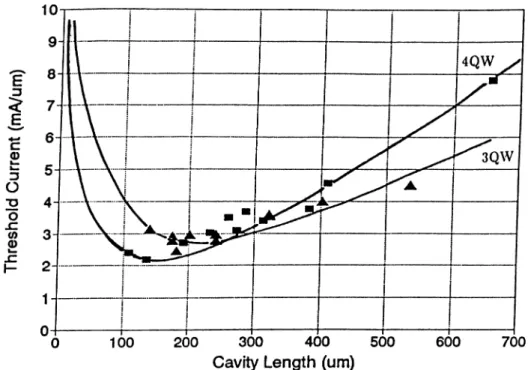
3.5 Optical Power O utput vs Forward Current Measurement System . 54 3.6 Cavity Length dependence of Threshold Current... 56
3.7 Plot of the Threshold Current Density versus Inverse Cavity Length. 57 3.8 Optical Power vs Current Characteristics of Sample-B8 ... 59
3.9 Inverse Differential Quantum Efficiency vs Cavity L e n g th ... 60
3.10 Experimental Set-up for Far-Field M e a su re m e n ts... 62
3.11 Lateral and Transversal Far Field Pattern of 3QW L asers... 63
3.12 Lateral and Transversal Far Field Pattern of 4QW L asers... 64
3.13 Near-Field Radiation Pattern Meeisurement S y s te m ... 65
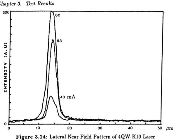
3.14 Lateral Near Field Pattern of 4QW-K10 L a s e r ... 66
C h ap ter 1
In tro d u ctio n to S em ico n d u cto r
Lasers
1.1
A H istorical P ersp ectiv e
The search technology of lasing micro-structures began with observation of stimulated light emission in a forward-biased p-n junction by four independent groups simultaneously in 1962.^”® This discovery of the laser diode triggered a great activity directed mainly toward finding new, reliable and powerful semiconductor structures. First breakthrough came with the development of ternary AlGaAs, leading Zh.I.Alferov, et al. from Ioffe Institute to demonstrate successful operation of first room-temperature semiconductor (GaAs/AlGaAs DH lasers grown by LPE) injection laser in 1970.® Then the development of quaternary InGaAsP single crystal alloy followed, resulting first room- temperature long-wavelength LPE grown InP/InGaAsP lasers at 1.1 pm by J.Hsieh,ei al at Lincoln Lab in 1976.^ Two years later, the operation of first room- temperature quantum well injection lasers having MOCVD grown GaAs/AlGaAs MQW structure was reported by two different research groups; N.Holonyak and D.Dupuis, et al.^ After three decades of effort, the laser diode has become a useful room-temperature device. And in the past few years, parallel to the advances in growth technology, great progress has been achieved in obtaining high-speed, low
threshold and high performance semiconductor lasers. Finally, the leist milestone in the semiconductor laser field has been recorded in 1987. It was demonstra tion of first room-temperature hétéroépitaxial CW GaAs/AlGaAs(MOCVD)- GaAs(MBE) laser operation shown by N.Holonyak (UIUC), Shichijo (TI) and Burnham (Xerox) separately.
The first visible laser diodes, based on InGaAlP materials, came on the market in 1988, extending potential uses of laser diodes to most of the mass applications in light-wave transmission previously addressed by He-Ne tubes. At 1.3-1.55 pm wavelengths, InGaAlP Icisers provide the basis for long-distance fiberoptic communications. In general, laser diodes with wavelengths over 1 pm, regarded as long wavelength, are more suitable for optical communication. Those with wavelengths under 1 pm are particularly used in optical information for data storage and optical sensing purposes as in compact disc players (A = 780 nm), laser printers and barcode scanners ( 650 < A < 780 nm).
Chapter 1. Introduction to Semiconductor Lasers 2
1.2
Lasing A ctio n in S em icon d u ctors
The word laser stands for light amplification by stimulated emission of radiation. Although, there exists a variety of semiconductor lasers differing in size, speed and power, essentially the same electronic action takes place in all of them. This lasing action can simply be analyzed by considering a basic semiconductor p-n junction. When an electron makes a downward transition from an upper to a lower energy level, an energy quantum is released in the form of light, i.e photon, as shown in a simple-two level band diagram of figure 1.1.a. This phenomena is said to be spontaneous in that each released photon acts independently. But if a monochromatic light source impinges upon the semiconductor, the electron in the upper energy level will act differently while the photon energy remains same as E2 — E \. Then, a photon is emitted as before
while it drops to lower state, but now, its timing is such that it synchronizes with the incoming photons (Figure: 1.1.b). For this reason, radiation is said to be coherent since all the emitted photons are in phase with the photon that has
Chapter 1. Introduction to Semiconductor Lasers
Current
hp
(a) Spontaneous Emission (b ) Stimulated Emission F ig u re 1. 1: Emission in a p-n junction laser diode.
induced the transition. In fact, the presence of the external photons tends to increase the downward transition. Therefore, electrons are in this way stimulated to produce additional photons, resulting in optical gain or amplification.
To arrive at lasing action, there must be more electrons in upper state than in the lower state so that the number of stimulated emissions must be greater than th at of the absorption transitions. So, a population inversion must exist in the system. However, this condition is not eeisily met in an ordinary p-n junction. Degenerately high doping at the p and n sides and also an extreme forward bias are needed to inject enough electrons and holes to put the quasi-Fermi levels at the band edges. High doping causes the band structure to be perturbed so as deep bandtails are formed which provides direct band-to-band transitions more likely to o c c u r . I t is desired that carriers in semiconductor must exhibit high radiative transition probabilities which is only satisfied in direct^ bandgap materials due to their energy-wave vector interrelation. Figure 1.2.a (from ref. 9) shows the band diagram of such a junction at thermodynamic equilibrium in which both
tOccasionaly, the lasing action was observed in indirect band-gap materials, but that was achieved under very specific experimental conditions (Nahory el at.; Holonyak,Jr.e< at., 1971)
Chapter 1. Introduction to Semiconductor Leisers
(a) Under thermodynamic equilibrium (b) Upon forward bias.
F ig u re 1.2: Energy band diagram of a p — n junction laser diode
electrons and holes within each band are in thermodynamic equilibrium whereas no equilibrium exists between electrons and holes. Upon forward bias, electrons are injected from n-side into the p-side through transition region and recombine with holes radiatively while releasing photons of energy Ai/.(Fig. 1.2.b) Therefore, to achieve lasing, separation of qu£isi Fermi levels, Efn-Ejp must exceed the photon energy which is approximately equal to the bandgap. Eg. These photons are then kept in the transition region to provide subsequent stimulated emissions.
In the given p-n junction model, however, there exist two problems. First, carriers injected to transition region diffuse away from the junction and this means a higher current is required to reach population inversion. Secondly, emitted light is excessively lost in the direction normal to the junction. One, therefore, needs an improved structure to concentrate injected carriers and emitted light near the junction’s active region. Such confinement can be achieved by constructing a double-heterojunction where a p-GaAs is sandwiched between a p and n Alj;Gai_xAs layer. In such a heterostructure minority carriers cannot diffuse away from the narrow gap region because of the potential step in GaAs/AlGaAs interfaces. Since Al^Gai.^As has a wider bandgap than GaAs, a potential barrier is created which provides excellent carrier confinement.
Chapter 1. Introduction to Semiconductor Lasers ·& a. a O •o c (0 m
F ig u re 1.3: Band Gap and Refraction Index variation in AlxGai_i:As.
automatically by the abrupt reduction of the refractive index outside the region. Since, as the AI content x of Al^Gai.^As is increased, its refractive index will decrease, the refractive index of the GaAs active layer is larger than the index of surrounding AlGaAs layers. In this way, the propagation of the electromagnetic radiation is optically confined within this slab waveguide geometry in the direction parallel to the layer interfaces. Refractive index and bandgap energy considerations of Al^Gai-^As are drawn in Figure 1.3.*
However, two other requirements are still needed in order to reach lasing threshold in a semiconductor Iciser diode; an optical cavity must be provided to build up the optical wave through positive feedback, and also the optical gain within the device must be greater than optical losses. This can be accomplished by using a resonant cavity consisting of two parallel mirrors, known as the Fabry-
Perot resonator. This cavity is usually established by cleaving the GaAs crystal
along the (110) planes. Then the cleaved surfaces will be perfectly parallel forming an ideal mirror. It is also possible to add dielectric coatings to these cleaved ends to control reflectivity and protect them from oxidation. The high reflectivity of a GaAs/air interface (~30%) gives optical feedback into the cavity
so that round-trip optical gain is achieved and, when it becomes sufficiently high to overcome the losses, the laser action results.
In the resonant emission only the longitudinal modes with a wavelength separation of A^/2L are propagated.^ In fact, the light wave at this lasing mode can also resonate back and forth transversely,t.e in the direction normal to the junction. The fundamental transverse mode is a sine-like standing wave with a
half-length equal to the transverse cavity length.
Chapter 1. Introduction to Semiconductor Lasers 6
1.3
Q u an tu m W ell Lasers
Optical radiation is guided by the slab waveguide geometry and amplified so that, above the onset of lasing, the optical output increases much more rapidly with drive current. It is usually the case that the thickness, d of the active (recombination) layer is less than the injected carrier diffusion length so that (if the heterobarriers are sufficient to combine all the injected carriers) it is uniformly excited across its thickness. As d is reduced to less than 1 //m, only the fundamental optical mode can be guided and a fraction of this mode energy (F) is contained within the active layer, a consequence of Maxwell’s equations applied to dielectric waveguides.”
In this respect, quantum-well (shortly as QW) lasers with their ultrathin active layers are employed yielding several superior characteristics such as,
• Reduction in laser threshold current density,
• Reduced temperature dependence of Jth·,^^
• Higher relaxation oscillation resonance frequency,
• Higher polarization stability,
• Higher differential gain with a narrow gain spectrum,*“' tExact derivation is given in “Propagation and Gain” section.
Chapter 1. Introduction to Semiconductor Lasers
In QW structures a series of energy levels and associated subbands are formed owing to the quantization of electrons in the direction of the quantum well thickness.*® This localization of carriers in ultrathin layers perpendicular to the layer plane is attributed to quantum size effect}^
The multiple quantum well structure which has a superlattice segment in its active region is achieved by modifying the core structure of QW lasers. Thus, upon bias, carriers are injected into the various GaAs wells that are separated by AlxGai_¡rAs barrier layers. By increasing the x content,i.e increasing the depth of walls, density of states in the cavity can be increased. This increased density of states leads to a corresponding lowering of the threshold needed for achieving population inversion.*® By considering both the selection rule in the electron-hole recombination and of the energy separation between the heavy and light holes in the MQW structure, it is expected that the optical gain for a TE polarized wave would be much larger than that for a TM as shown experimentally by Okamoto.*® This can be stated as polarization-dependent optical gain.
Until 1981, MQW lasers studied were not containing higher than x=0.3 content in Ala;Gai_j;As barrier layers. It was Tsang*® who reported that using of larger AlAs composition in the cladding layers results in better optical confinement and also use of larger well-to-barrier ratio results in lower threshold.
By now, the idea of MQW has already been applied to its two- and three- dimensional conjugates i.e. quantum wire and quantum dots.
Chapter 1. Introduction to Semiconductor Lasers
I
I
K)i
Ri Rj
F ig u re 1.4: A simple Fabry-Perot Resonator model of Laser Diodes.
1.4
T h eo retica l B ackground for Q W Lasers
1.4.1 P ro p a g a tio n and G ain
A common way for formulating basic gain equations in a laser diode is to construct the simple oscillator model of a Fabry-Perot resonator enclosed between two reflecting planes. As shown in Figure 1.4, resonator employs two confronting mirrors with reflection coefficients Ri and R2 where the space between filled with a light amplifying material of refractive coefficient, h r. There are three
kinds of modes describing the oscillations of the electromagnetic field in this 3D rectangular resonator. The wavelength of radiation concentrated in these modes can be found from the standing wave condition inside the active layer:
■ '.=...O D
where dr, Wr and L denotes respectively the thickness, width and the length of the resonator. The indices m, s and q are then the numbers that characterizes the type of the mode; longitudinal, lateral or transversal. If we assume only longitudinal modes are propating (q=s=:0), then above equation reduces to,
A/2 m —— = L
riR (
1
.2
)here m = l ,2,3, . . . corresponds to order of longitudinal modes propagating inside the laser. It follows from equation 1.2 that the phase condition for the resonance oscillations to occur is satisfied when there exist an integral number of half wavelengths between the end mirrors. Differentiating this equation with respect to A and substituting the value of m from above, give the separation between the
Chapter 1. Introduction to Semiconductor Lasers
adjacent longitudinal modes,
dX =
2 n « L [l-(A /n fi)(d n « /d A )]
Then the spacings between succesive longitudinal modes on the spectral characteristic can be found as,
A2 A2
AA = (1.4)
2L{nn — Xduft/dX) 2Lna
where uq is the group index of refraction.
In the given resonator model, the plane wave propagating in z direction can be expressed using the condition of equation 1.2 as,
.i · 2imRZ.
exp[- -] · exp[(g - ai)z] (1.5)
where A is free-space wavelength, g is gain and or,· is the coefficient of internal losses. For a standing-wave oscillation to occur, the wave amplitude after a round-trip should be equal to its amplitude, which can be interpreted as,
R1R2 exp[— · exp[(g - a ,)2L] = 1
Hence the amplitude condition for the oscillations to occur is,
RxR2 exp[(g - oci)2L] = 1
and from here threshold gain can be written as, 1 , 1 Zth = or,· + —
In-(
1.
6)
(1.7)(
1.
8)
2L R1R2The reflection coefficient at the semiconductor/air boundary is generally defined
as R = · If the reflection coefficients of the two resonator mirrors are made equal to the reflection coefficient at this boundary (Ri = R2 = R,y then
the threshold gain given by equation 1.8 can be put in the form of 1 , 1
gtA “ ~
in which the end losses, ore„j term stand for side-mirror losses.
(1.9)
^Calculation of reflection coefficients for varying thickness of active layer is discussed by Ikegami.^®
Chapter 1. Introduction to Semiconductor Lasers 10
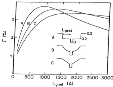
F ig u re 1.5: Power law GRIN profiles drawn for a MQW Iciser
1.4.2
O p tical C on fin em en t F actor
The efficiency of electromagnetic field confinement in the active layer is described by confinement factor, P, which is defined as the ratio of energy flux confined within the active layer to the total energy flux of the radiation generated in the laser. Confinement factor is strongly dependent on the geometry of optical cavity and refractive index variation inside. Basically, it can be defined by an equation of the form,
I Si P dx
Until it is first proposed by W.Tsang,*® heterostructure lasers were limited to well designs with abrupt step index change at the boundaries. He reported graded index separate confinement heterostructure (GRIN-SCH) profile while achieving separate carrier and optical confinement in parabolically graded-index waveguide. Various index profiles can be described using the so-called power law index changes;
n{r) = - 2 A ( - r y ^ \ \ r \ < w / 2 (1.11)
w
where w is the total width of the active layer, r is the distance from the center of the waveguide, p is the exponent of the power law, A = {n·^, — n,c)/n^ with
Chapter 1. Introduction to Semiconductor Lasers 11
F ig u re 1.6: Variation of P with respect to GRIN profile
riyj, lie are the refractive indexes at the well and cladding layers respectively. In
figure 1.5 resulting index profile is drawn for w=4000 A , = 3.4516 for x = 0.2 and tic = 3.1376 for x=0.7 in Al^Gai-xAs. Notice that in the limit of very large p (~100), profile approaches that of the regular SCH.
McIlroy,et calculated the values of P for varying guiding layer thicknesses of three main index profiles. The variation of P with power, p changing from infinity to unity (y4 : p ~ oo, B : p ~ 2 , (7: p ~ l ) i s given in figure 1.6 for a well width of 100 A . It is worth noting here th at the linearly graded profile when p is equal to unity also describes the profile and confinement behaviour of the structures used in this study.
Figure 1.6 also indicates the difference in confinement behaviour between a separate confinement heterostructure (SCH) and normal abrupt junction heterostructure lasers. Confinement factor, P decreases rapidly when the guiding layer thickness is made less than 500 A where the total active layer thickness start to become comparable with the wavelength of the radiation in the semiconductor.^^ This means that any increase to be made in the quantum well width will highly effect the optical confinement in this regime. Therefore in abrupt junction heterostructure Icisers optical confinement is strictly dependent
Chapter 1. Introduction to Semiconductor Lasers 12
on quantum well width(s). However, SCH lasers are generally designed so that the guiding layer thicknesses are made larger than 0.1 pm, thus the degree of optical confinement is mainly determined by the geometry of the guiding layers as shown in the figure. If we name total confinement factor as r„et and define,
r'nei — rc o n / "h r"toe//
(
1.
12)
where Fcon/ refers to confinement in the guiding layers confining core well arrangement and r„,e// is the contribution by quantum well(s) to the r„et, then in the cases where guiding layer thickness is larger than 0.1 pm the Tconj term becomes dominant and the second term can be neglected. Therefore if we have a core MQW arrangement at the same time, then the net confinement factor is independent of the number of wells.1.4.3
T h resh o ld C u rrent D e n sity
The gain, g in equation 1.5 is referred as material gain. If it is uniformly distributed across the active region (g(x) = g), then the modal gain,^, confined within active region can be expressed as
a = r g (1.13)
by using confinement factor P. To achieve at lasing for the fundamental transverse mode to be excited, the following threshold condition should be satisfied,^^
Go — r*oS — r'S t/i — "b ^end (1.14) where gj/, denotes threshold local gain, Oend is the second term in equation 1.9 corresponding to end losses and a, is the internal losses which is given by the sum,
a,· = FoOifc + (1 - ro)ao„t + a , + »c (1-15)
Here, a , and Oc , a / J and a„ui are the coefficients representing optical scattering losses in the active region and in the cladding layers, free-carrier absorption in
*The free carrier absorption coefficient for GeiAs^“' at room temperature may be written as
Chapter 1. Introduction to Semiconductor Lasers 13
active layer and in the cladding layers, respectively. Therefore, in practice it is quite difficult to separate the different contributions to a,··
The equation for the threshold current density Jth of (AlGa)As broad-area Fabry-Perot double heterostructure (DH) Itisers is given by ,
Jth = -Vi
1
J o + + (1 — Г)оГои< -f- O', - f Qic - f Qiend) + JN d-jp (1-16)
where and j p are densities of electron and hole leakage currents, and a is given as 5 X 10~^ cm pm / AJ'* Coupling loss, Oc, may be assumed negligible if cladding layers are thick ( ~ 0.2 /zm) and Oout can be taken as ~ 10 cm~^. Thus, a,· is typically found around 10-20 cm~^. The equation given in 1.16 can be written more specificly using a,· as,
d d
7/,· Щ ¡3 ГOti + ----j j i 0 r L L with the gain-current relation assuming the linear form,
Smaa: ~ 0 ( ,J n o m Jo')·
(1.17)
(1.18)
In 1.17, we can call the first term as intrinsic term, the second as internal loss term and the last one as mirror loss term. Here it is seen that main contribution to Ji/i comes from the first intrinsic linear term if active layer is not much less than 1000 For the case where d ~ 700 Л, mirror and internal loss term start to become effective due to decreased optical confinement factor Г. The term Jnom in equation 1.18 is called as nominal current density which is related to actual current density J as Jnom — ^i{J
Using the multiple quantum well structure as an active region, several research groups have demonstrated room-temperature continuous-wave operation of lasers with very low threshold currents in the range 0.88-1.0 mA to date.^’^’^® Uncoated MQW stripe-geometry lasers with thresholds as low as 1.0-1.6 mA have also been achieved by growth on ridge-structure.^® The progress has been made, in large part, by the optimization in MQW design and device structure.®®
Chapter 1. Introduction to Semiconductor Lasers 14
F ig u re 1.7: Optical Radiation from a Ridge-Waveguide Laser.
1.4.4
N ear and Far O ptical F ield D istrib u tio n s
Active layer structure is rectangular rather than cylindrically symmetric.(Fig. 1.7) Emitted beam from the active layer is refracted and takes the form of a vertical ellipse (far-field pattern), whereas it has the shape of a horizontal ellipse (near field pattern) on the surface of the mirrors. Therefore, a diode with an acceptable light output has two beam-divergence angles. The ratio between that two angles taken perpendicular and lateral with respect to geometry is called as aspect ratio which is given by ^ In general, the nearer this ratio is to unity the better, then the beam is more circular.
1.4.5
C oupling b etw e en Q uantum W ells
In addition to optical absorption and stimulated emission, quantum states of electrons and holes is also observed to couple via tunneling for a quantum well of GaAs bounded by thin Al^Caj.^As barriers.^* This coupling of quantum wells is due to overlapping phenomena in so-called communicating wells adjacent to each other. This may lead to a series effect in multiple quantum wells thereby increasing the threshold current density.’* However, the 150 A barrier thickness of the laser used in this study prevents quantum wells from coupling as also verified by Dingle, et
C h a p ter 2
F ab rication
2.1
P ro cess S teps
The fabrication of laser diode involves many steps, each of which must be optimized to achieve acceptable performance with reliable and repeatable manufacturing yields. (Table: 1 ) Subsequent sections of this chapter are concerned with specific stages followed in the fabrication of a ridge-stripe type MQW laser diode. At the beginning of each section, an overall view of that processing step is given. Then experimental set-up and parameters chosen are described. Finally, a respective discussion related to processing method is included at the end.
Table: 1 L aser D iode P ro c essin g Flow C h a rt Chapter 2. Fabrication 16 • C L E A N IN G • Spinning Photoresist • P H O T O L IT H O G R A P H Y • D R Y E T C H IN G (R IE ) • Anodic Oxidation • P E C V D • L IF T -O F F • P - ty p e M E T A L L IZ A T IO N
• Annealing and Thinning
• N -ty p e M E T A L L IZ A T IO N
Chapter 2, Fabrication 17
F ig u re 2. 1: Convention for identification of flats on wafers.
2.2
Sam p les
2.2.1 W afer sp ecifica tio n and clea v a g e
The laser diode fabrication typically begins with the form of a circular GaAs "wafer” 2 to 4 inch in diameter and approximately 0.5 mm thick. These wafers are readily provided with the cited surface orientations, thereafter epitaxial layer arrangement (for example a MQW structure) is grown on the GaAs substrate. Since it would be difficult to process the whole wafer, and also a complete waste to spend it in a single process run, it was preferred to cleave wafers to separate into appropriate pieces. To do that, a short groove was opened on the front surface by precisely drawing a diamond-tipped scribing tool along the desired breakage line at the primary flat edge of the wafer. Primary flat is the long straight-line region along the periphery of the wafer and positioned originally to identify crystalline directions lying within the surface plane. The relative orientations of the primary and secondary flats indicate both the wafer type (n or p) and surface orientation as shown in Figure 2.1.^^ For (100) oriented wafers of our interest, the primary flat along the edge of the wafer is a (Oil) plane, and the normal to this flat is defined by [Oil] direction.
Chapter 2. Fabrication 18
Then, to break the wafer, a small stress (to avoid damaging the structure) is applied on one side of the scribe line and wafer is bent to cut into two pieces. However, since GaAs is very brittle and has a tendency to break easily in arbitrary directions if not cleaved in the proper direction, a knowledge and understanding of the wafer surface orientation and respective indices are essential for a succesful breakage. This idea based on the fact that crystal GaAs wafer, when mechanically stressed at room temperature, is cleaved most readily on the (110) planes.^"* This feature completely comes from the nature of GaAs crystal structure. It is, basically, a result of variation in atomic packing density for different planes in which packing density and available bonds decrease as we go from ( 111) to (100) to (110). Therefore samples with perfect rectangular geometry are obtained by cleaving (100) oriented GaAs wafers perpendicular to the major axis, in the [Oil] direction.
2.2.2
M Q W W afer In sp ectio n
Process samples consisted of pieces of having approximately 2 cm^ area obtained by cleaving nominally around 400 fim thick (100) oriented 3” (80 mm in diameter) GaAs MQW-wafers. These molecular beam epitaxy (MBE) grown MQW wafers were supplied by University of Eindhoven, the Netherlands. The device structure of the GaAs/AlGaAs MQW laser diodes used for this research is given in figure 2.2. The micrograph taken by JSM-6400 SEM shows that the interfaces are sharp and the layers are uniform. In the figure, aluminum contents and thicknesses around the active layer are also indicated.
The structure is grown by MBE on an n-doped (100) GaAs substrate starting with a substrate temperature of 580 °C and reaching up to 800 °C when growing Alo.7Gao.3As cladding layers. The core active layer consist of a quantum well arrangement of three or four 70 Â thick undoped GaAs quantum wells seperated by 150 A thick Alo.2Gao.8As barriers, which is centered between two 0.2 pm thick AlxGai_xAs optical guiding layers having linearly graded A1 profile(x:0.2^0.7). This is then sandwiched between Be-doped p and Si-doped u-type Alo.7Gao.3As
Chapter 2. Fabrication 19
X 10.000
cap- layer cladding layer ^ - -M Q W buffer-layer cladding layer substrateF ig u re 2.2: Layer Structure of the MQW samples
outer-cladding layers. The aluminum fraction in the cladding layers is taken as 0.7 so that the light and carrier confinement are sufficiently high. The thickness of these cladding layers are around 1 pm for p- and 1.25 /xm for n-Alo.7Gao.3As layer to ensure low waveguide losses.
As seen in the cross-sectional figure, n-t}'pe cladding layer incorporates a Si doped 500 A thick superlattice buffer-layer 0.25 pm beyond the active layer, which is made up of repetation of ten period 25 A Alo.7Gao.3As/25 A GaAs layers. The 0.7 aluminum content of cladding layers decreased down to zero in 0.3 pm distance away from both sides. Finally, layer arrangement is terminated by growing a 0.75 /xm p-|-GaAs capping layer at a substrate temperature of 500 °C for the p-type contact. The doping density of the top cap-layer is kept high at about 3.56x10'^ for the nonalloyed electrode consisting of T i/P t/A u to form a good ohmic contact.
Chapter 2. Fabrication 20
2.3
C leaning and Surface Preparation
2.3.1 S am p le C leanup
To prepare samples for the application of photoresist, a sequential multistep rinsing treatment has been applied, the front and back sides of the wafer is cleaned chemically and mechanically. First, samples were immersed in hot TriChloroEthane (TCA) bath for 2-3 minutes. One method applied to ensure TCA cleanup has been made thoroughly was holding sample just above the solution to the TCA vapors and to check if it evaporates uniformly from the surface. This is a particularly clean method as only distilled vapors act on the sample.
Secondly, a hot bath of acetone^ was applied for two minute duration. During aceton bath, it seemed that cleaning the sample surface using a clean cotton tipped tool worked quite well to clean out all residual materials. This method can be stated as a mechanical brushing technique and has been proved to be very effective in removing particle contaminants by overcoming the adhesion forces.^® But, for the very dirty samples (re-used ones) two-bath immersion treatment of first aceton bath for 5 min and 2 to 3 min in a second was preferred. In the third step, dipping for one minute in cold Isopropanol followed. At this stage, it is also possible to apply a 18 Mii-cm deionized (DI) water spray rinse where this step was skipped in some process runs. Finally, samples were dried under continuous Nitrogen(N2) gas flow. Thus a clean and dry surface is provided to ensure good photoresist adhesion in the next step.
One can also make sure that all the chemicals (that might have penetrated into sample during cleaning) are evaporated by putting the samples into an oven for 1-2 minutes at about 80-90 °C afterwards. This can be termed as dehydration
baking and helpes to improve adhesion of resist by creating more mechanical-
chemical bondings on the surface.
The only precaution must be taken in following this procedure is that one should not allow the wafer to become dry before going to subsequent rinsing, as
Chapter 2. Fabrication 21
the evaporation of one of the solvents would leave behind residues that may not be soluble in the solvent used in the next step.
It is known that when a clean GaAs wafer is left open to air, an oxide layer as thick as 30 A grows in four days.^® Moreover, a carbon overlayer is then formed when the steady-state thickness is reached. This thin oxide-carbon layer at the interface, highly affect the contact performance especially in metallization giving a poor contact quality and failure in reproducibility.^®
2.4
P h o to lith o g ra p h y
2.4.1 A n O verview o f P h otolith ograp h ic P rocess
Photolithography is the name given to complete process of replicating the mask pattern on the wafer surface using photoresist as the masking element. Photoresist, shortly as PR, is basically a photosensitive polymeric material commonly supplied in liquid form. This process starts with deposition of a thin photoresist layer over wafer surface by spin coating. To do that, the wafer is held on a vacuum chuck and drops of liquid photoresist is dispensed onto wafer surface. While resist is laying down, the spinner is spun at high speed to produce a uniform resist film across the surface by means of centrifugal forces spreading resist outwards.
The thickness of the resist coated, depends on its viscosity and is inversely proportional to the square root of the spinning speed.®^ Therefore, spinner is rotated accurately at a predetermined speed for a specified time. Spin time is adjusted to match the duration in which PR thickness is stabilized. Resist must be deposited thick enough (at least 0.3-0.4 pm) so that it can withstand etching to avoid resist erosion. This sets a lower limit on photoresist film thickness.
Next, a drying step referred as sofl baking or prebaking is applied by simply heating the PR coated wafer in the oven in air atmosphere. Softbaking is primarily used to harden the resist by removing the solvent and water remaining
Chapter 2. Fabrication 22
F ig u re 2.3: Photolithography using the negative and positive photoresist
in the film after spin-on. This removal, while improving adhesion, decreases the resist thickness.^ After that, mask alignment and exposure step is carried out. Mask is a few mm thick, square glass plate with one of its faces containing the ridge-pattern to be generated on wafer surface.
Using mask aligner, wafers were placed under mask onto an adjustable xy stage for alignment. In separation mode, the wafer is carefully positioned within a few micrometers of the mask. After alignment, the face of the mask covered with pattern is brought into direct contact with the wafer, in the contact printing mode. But here, closeness of the mask and wafer may cause damage and contamination of the mask. Following alignment, the photoresist is exposed through the mask with high-intensity ultraviolet light from a mercury lamp.
In subsequent developing stage, the exposed areas of the resist is removed chemically in diluted developer solution. Photoresist acting in this manner is called as positive resist and a copy of the same mask pattern remains on wafer surface.(Fig. 2.3) Negative resists, on the other hand, acts oppositely and negative image results after washing away the irradiated or shadowed regions. DeForest^^ discusses origin of this feature related to exposure mechanism and chemical reactions, postulated first by Sus and Levine in 1944.
Chapter 2. Fabrication 23
After exposure and before development, a second bake referred as posthake (sometimes it is made after development and this time called as hardbake) is also possible to add advantages of hardening resist, increased contrast and better adhesion. Postbaking increases the resistance of the resist to the etching process, because hardened resist is rather difficult to remove as solvent penetration becomes restricted. However, this may cause problems in lift-off applications and therefore not preferred.
2.4.2
P ro cess D eta ils
The masking material used is 0.1 /im prefiltered AZ-5214E (American Hoechst) positive photoresist. This is one of the new resists whose spectral absorption peak is at about 360 nm, so it is ideally matched for mercury i-line (365 nm) photolithography.
Resist film with a thickness of approximately 1 pm were obtained by spinning at 5000 rpm for 30 seconds. Just prior to application of resist 100% HMDS (hexamethyldisilazene) were applied to cover the wafer so that it promotes the adhesion of resist to wafer. While doing that, HMDS was left 5-15 sec before spinning, depending on the level of adhesion needed. After PR dispense, it was seen that some increase in PR thickness inevitably occurs at the edges of the wafer probably due to surface tension of the liquid. However, these regions helps a lot in determining the exact distance where this regions comes into contact first with mask in alignment.
Following the resist application samples are soft-baked at 90 °C for 40 minutes. Since the degree of solvent removal, temperature and time of the softbake directly impact on exposure parameters, these are critical parameters requiring optimization first. In this respect, it was seen that between 90 and 100 °C is an ideal range for temperature, and by achieving 100 °C, photoresist starts to reduce its apparent sensitivity as indicated by E llio tt.T h is degree is optimized for softbake time changing between 30-40 min.
Mask alignment and exposition steps were carried out by following con ventional photolithography techniques in Karl-Suss MJB-3 Mask Aligner. The
Chapter 2. Fabrication 24
mask used was comprising parallel, 5 and 12 pm wide^ dark lines (stripes) on a clear background for positive photoresist application. In exposition, aligner was brought to soft contact printing mode whereby a reduced vacuum is applied to prevent the extreme pressure between mask and resist. Then, sample is aligned under mask so that stripes will be parallel to major axis of the wafer to simplify cleaving and seperating procedure in the final step.
Samples were then exposed to define ridges on the sample surface under 12 mW-UV for about .38 seconds. For 12 mW exposition, it was observed that resist is underexposed if exposition time is decreased under 33 sec and there exists a tendency for the pattern formation to be incomplete. On the other hand, overexposition occurred with extreme loss of pattern if this interval is increased to a value as high as 44 sec. This behaviour can be attributed to penetration of excessive scattered light under the mask edges by the time and exposition of the region not directly irradiated by the light source.
Developing step is completed in one minute in AZ-400K Developer/DI water bath(l:4). Resist dissolution rate in developer is found to be strongly dependent on developer dilution ratio and softbaking parameters. If developer concentration is increased, for example to 1:3, developing time is observed to reduce as well, but leaving a more distorted line-width geometry with loss of image dimension due to increased speed of the reaction. However, when samples are left further in the developer bath well after stripes became clear on the surface, overdeveloping resulted in washing away most of the pattern and causing failure of the lithography process.
After that, samples are rinsed in DI water. Postdevelopment rinse is a required complementary process since removed photoresist residues, or scums, may attach *
* Narrow stripes on the order of a few microns, ensures that the optical wave exhibits zero- order transverse mode behaviour and remains located centrally on the stripe. This can be expressed in terms of active layer thickness for selection of transversal modes in the Iriser as,
dm = m ^ (njt2 4 i ) -1/2
It means that if the thickness of active layer d becomes smaller than dm, then the m-th order mode is no longer confined within the laser cavity.
Chapter 2. Fabrication 25
back to the surface and can cause blocking etching in the next step. It is obvious that the resist dissolved in the developer solvent will accumulate as it is used repeatedly. Therefore replacing with new one regularly is necessary to minimize the effect of contamination. Rinsing also prevents resist erosion which may take place in the unexposed areas that absorbed developer solvent.
There exist many other factors that must be considered in a specific optical lithography process. The ones related to laser diode fabrication can be summarized in three separate parts forming a basic lithography system;
• A lig n m en t a n d E x p o su re. Minimum feature size that can be transferred primarily depends on the quality of imaging system, that is resolution of aligner and on the wavelength of the light. Resolution of the aligner can be expressed as, R = kX/ NA ,where k is around 0.8 and numerical aperture, NA is 0.4 with A=320 nm for MJB-3. •
• M ask. For a reproducible processing mask must be high quality with no defect or dislocations both in glass surface and on the pattern. It is also desired for mask to be highly chemically resistant to glass- and mask cleaning solutions. Alternatively, it must have high optical transmission in the wavelength range used to expose photoresists.
• P h o to re sist a n d A ssociated C hem icals. All the chemicals (including photoresist) must be clean from the dust, dirt and the other particles. For the resist, it is often necessary to filter futher as it is done in this process. It must first be chosen to match the resolution of the pattern to be transferred to be able to form fine patterns in low dimensions.
Chapter 2. Fabrication 26
2.5
E tch in g (D ry)
2.5.1 E tch in g T ech n iqu es
After pattern is defined using resist layer on the front surface, this geometry is transferred onto underlying semiconducting structure by means of etching. Etching process preferably acts in a way to remove any surface material not protected by hardened resist.
Etching can be performed with wet- and dry-etch (gas plasma, ion, or reactive ion etch environment) methods. Wet etching basically uses liquid based (wet) etchants to act. It proceeds at the surface of the GaAs through some ordered chemical reactions: first surface is oxidized, then the oxide (Ga20 , Ga203, AS2O3, AS2O5, etc.) is dissolved while removing some of the Ga or As atoms from the surface. Chemical etches for GaAs normally consists of an oxidizing agent (commonly H2O2) mixed with an acid (like H2SO4) or base, as ammonium hydroxide, that reacts with oxides of Ga and As. Examples of etching solutions for some materials can be given as HCI/HNO3 (3:1) for gold, HCI/H2O (1:4) for aluminum, diluted HE and H3PO4 for Si02 and Si3N4. Related to GaAs wet etchants an extensive study has been summarized by Adachi and Oe.^*
Wet etching tends to be an isotropic process^, etching uniformly in all directions resulting an ordinary hole-like figure. The characteristic wet-etch behaviour of etching laterally at and below the resist layer through substrate is called as undercutting. There is no standard by which to measure good or bad undercut: it is just a function of the need of the process and sometimes it can be desired at some levels to get a sloped side-wall. Undercutting can be used as a degree of anisotropy to determine fidelity of pattern transfer. This degree is defined by aspect ratio which is basically given as etch-depth to width ratio. In laser diode processing, anisotropic profiles with mirror quality vertical sidewalls which give rise to high aspect ratio values are preferred. Figure: 2.4.a shows the Scanning Electron Microscopy (SEM) picture of a typical isotropic *
*Wet etching processes along certain crystal planes of crystal materials may produce anisotropic results.^*
Chapter 2. Fabrication 27
F ig u re 2.4: Comparison of Wet and Dry etch profiles by SEM.
wet-etching of Hydrogen PeroxiderCitric Acid:DI Water (1 gr:10 gnlO ml) into n-GaAs (2x10^®)· Notice the excessive loss in the width of the (initially) 12 pm ridge pattern due to undercutting.
Highly anisotropic etching profiles with near-vertical sidewalls can be obtained by dry etching by avoiding the characteristic undercutting problem of wet processes. For comparison, the obtained profile of the same structure after dry etching in CCI2F2 plasma (RF power: 54 W, pressure: 0.8 Pa, gas flow: 10 seem) is also shown in the figure 2.4 where the time was kept constant at 15 min for both processes. Therefore, although rapid etch rates can be performed easily using wet etchants, when directionality and material selectivity is considered dry etch is preferred. The word selective is given as a comparison for etches that remove one material faster than another.
Reactive ion etching (RIE) combines other two dry-etch processes; plasma and sputter etching. In plasma etching, wafer is immersed in a gaseous plasma created
Chapter 2. Fabrication 28
by RF excitation in a vacuum system. This plasma contains ions which etch the wafer. Sputter etching uses energetic noble gas ions such as Ar+ to bombard the wafer surface and occurs physically. RIE, utilizes both chemical reactions in plasma etching and surface excitation processes of physical sputtering. In reactive ion etching, a gas such as CF4 is introduced into a reactor with two parallel electrodes across which a radio frequency(RF) voltage is applied. RF is primarily used to obtain higher degrees of ionization and achieve better control over ion energies. The RF voltage causes the reactive gas to break down and form a plasma of ions, radicals and reactive atomic species as a glow discharge in an electric field. This field appears as a steady-state electrostatic force across a thin charge-free region between plasma and the electrodes ^ called the dark sheath. As ions enter this region, they are accelerated towards lower electrode by this built-up electric field and impact on the wafer surface with high energy (reversely, electrons are decelerated). As a result of directed, energetic ion bombardment, reactive neutrals created in plcisma enhances etching in the direction perpendicular to the surface.
2 .5 .2
LE-301 RIE S ystem
Dry etching of submicron geometries is being handled today with RIE (cathode coupling), plasma etching (anode coupling), magnetron RIE and ECR (Electron Cyclotron Resonance) etching systems. In our process, dry etching was performed by using a Leybold-LE 301 parallel plate (planar) reactive ion etching system with a water cooled lower electrode that is powered by an RF source operating at 13.56 MHz. Figure 2.5 shows the descriptive model of RIE system indicating the mechanical rough pump, roots blower and the turbo pump. Grounded top electrode is generally designed to be much larger than the bottom one where the variable distance between can be adjusted up to 6 cm. Process chamber is pumped mainly by TMP-450C Turbo pump to achieve a base *
*The strength of this field can be expressed as, ^ . where Va, V c and Aa, Ac
Chapter 2. Fabrication 29
M E C H . P U M P
pressure in the order of 10“® mbar which leads to highly reproducible processing. In operation, the roughing valve is opened first, and the mechanical pump lowers vacuum chamber pressure to an intermediate vacuum level of a few pascals. When this point is reached, turbomolecular pump is operated to achieve high vacuum.
Wafers are inserted into load-lock chamber first, then transferred to the main etch chamber through an arm followed by vacuum pulldown. The gases are then bled into the chamber and rf power is turned on automatically, resulting in a glow discharge that produces plasma. The vacuum level achieved for our process is less than 1 Pa. Process parameters (time, pressure, rf power, gas type and flow, etc.) are given to system through a keyboard in the front panel. System, then, fully automatically adjusts the desired parameters to perform etching.
Chapter 2. Fabrication 30 е<г> г
1
5ij G5 70 75 30 S 5 P r o g ramm i n g : Avg Н г = 1 4 ,е 8 £ Л 14 1 2 10 8 e 4 2 0 Х І 0 0 0 C u r s o r s : Ж\/е r t 7 A M; 1 4 , 6 8 2 R: 1 4 , 6 8 8 Д: - 6 Ho r i z7um @74 @68 6 R e s o l u t i o n ; H i g h F ig u re 2.6: Dektak-Profile after etching2.5.3
P rocess D esc rip tio n
The ridge waveguide, was then formed by etching away top layers with dry etching using pure Freon-12 (CCI2F2) as the reactive gas. Predetermined value of CCI2F2 gas flow was 4 seem. A self bias voltage as high as 300 V was used for these experiments where the electrode spacing held constant at 60 mm. Pressure was kept at 4x10"^ m bar(=0.4 Pa). Initially RF-power has been set to 46 W but during the process it reached to 54 W value. A multistep etching has been applied while etch depth was detected during etching. Etching was stopped about 0.4 pm
above the active layer (graded index part of the cladding layer) which results in good lateral-mode confinement for waveguiding purposes. The magnitude of etch depth obtained after the dry etch process was measured by using DekTak-3030ST Surface profilometer as given in figure: 2.6. Accuracy in measuring etch depth is necessary in order to determine exact depth and profile obtained. In this respect, SEM can also be used with its ability to monitor profile uniformities within a precision level down to 50 A (Fig. 2.7)
One important point that deserves special attention here is related with over etching. This problem occurs when etching extends beyond a point at which
Chapter 2. Fabrication 31
X5000
F ig u re 2.7: SEM-Profile after etching
structure has been over-etched down to the active layer. Over-etching into the active layer results in introducing traps in the energy gap of the active region, due to bindings with amorphous oxide at the interface. These traps, in turn, cause non-radiative recombinations at the sides of the ridge, giving rise to high leakage currents and leading process to fail. Therefore, it is necessary to adjust parameters carefully to achieve desired depth and observe the level of depth etched with accuracy during etching. In this way, etching was performed so that remained thickness of the cladding layer above the active layer is as small as possible. However, there is a lower limit for this thickness as it must be large enough to cause reflection of the light inside the ridge for lateral optical confinement. Therefore, this level was determined to be 0.4 pm for our purposes with considering that it will reduce down to 0.1 pm after oxide deposition steps.
The only problem arose in etching with Freon-12 was excessive etching times reaching up to one hour. Although it was a must to spend that much time to etch 0.7 /zm depth with this recipe, this must be avoided to give less damage to the samples. It was also seen later on that this time interval can be reduced to 15-20 minutes and selectivity down to l.T by using CI2/BCI3 plasma as the reactive geis. Etching data related to CI2 based plasma is presented in a later section.
Chapter 2. Fabrication 32
n-GaAs(IOO) Etch Rate Determination
PressurerO.8 Pa RF;54W CC12F2;10sccm
105 110 I I B 1 2 0 1£ B Bch Depth o Etch Rate
(a) Obtained Profile after etching in CCI2F2 (b ) Plotting of all results. F ig u re 2.8: Etch Rate Determination
2.5.4
E tch in g A n a ly sis
In etching, by varying the process parameters and set-up, profiles with different degrees of anisotropy can be obtained. The issue here is to produce desired geometry by successfully determining the neeeded recipe for RIE. But, since the result of a specific etching process may vary from system to system, or even, machine to machine, several recipe were tried in order to understand basic etching properties (etch rate, depth, uniformity, etc.) of LE-301 RIE system. However, the power of this approach should not be underestimated as our progress in etching optimization for controlling over etch profile, arose from those many trial-and-error experiments. In this respect, etch outputs were studied versus changes in process parameters such as applied bias voltage, pressure, power level, gas percentages in the total flow.
E tch T im e v ersu s E tc h D e p th . General approach to analyse an etching result is to monitor surface profile and to determine etched depth by means of a profilometer or a scanning electron microscopy (SEM). Figure 2.8.a shows such a profile taken by DekTak Profilometer after etching n-type (2 x 10’*) 100-GaAs under 10 seem CCI2F2 flow. For the same recipe, a series of etch depth data was recorded at different etching times to map Freon- 12 etching
Chapter 2. Fabrication 33
Etching Rate Data of CCI2F2 Plasma
Pressure:0.8 Pa Gas Flow:20 seem
n-GaAs(IOO)
r>-GaP(111)
SI
F ig u re 2.9: Etching of GaAs, GaP and Si under CCI2F2 plcisma
behaviour.(Fig. 2.8.b) The etch rate can be first calculated simply from the slope of the line as 1500 A/min. Or, alternately, etch rates for every point can be determined and then an average etch rate value can be taken. This approach is illustrated on the right hand side of the graph where resultant etch rate is slightly less than 1500 A/min this time. This etch rate value was recorded for future reference, however, it is better to use only in the calculated time interval where the relationship is linear.
E tc h R a te s o f D ifferen t M a terials. For comparison etch rates of different materials at varying self-bias voltages were studied as shown in figure 2.9. Although increased etch rate values are recorded for increasing voltage, notice th at etching of GaAs tends to saturate around 2000 A/min while for GaP it still continuing to increase. However, at this pressure and flow conditions etching of silicon is seen to be acting very slow.
O xygen P la sm a R e su lts. In addition to CCI2F2 plasma, oxygen plasma has also been studied. The applied RF-power vs self-bias voltage relationship of both plasmas are given in figure 2.10. As seen, after about 80 watts applied both plasmas respond similarly by creating same bias level. For comparison, different materials have been etched in both O2 and CCI2F2 plasma under same conditions (Pressure: 0.8 Pa, RF Power: 74 W, Gas Flow: 20 seem, Self-Bias Voltage: 400 V). Obtained etch rate values are tabulated in the next page.