Li Chong, Xue Chun-Lai, Li Chuan-Bo et al.
INSTITUTE OF PHYSICS PUBLISHING SEMICONDUCTOR SCIENCE AND TECHNOLOGY Semicond. Sci. Technol. 19 (2004) 1259–1262 PII: S0268-1242(04)81049-6
High-speed characterization of solarblind
Al
x
Ga
1
−x
N p–i–n photodiodes
N Biyikli
1, I Kimukin
2, T Tut
2, T Kartaloglu
1, O Aytur
1and E Ozbay
21 Department of Electrical and Electronics Engineering, Bilkent University, Ankara 06800, Turkey 2 Department of Physics, Bilkent University, Ankara 06800, Turkey
E-mail: [email protected]
Received 21 May 2004
Published 16 September 2004 Online at stacks.iop.org/SST/19/1259
doi:10.1088/0268-1242/19/11/008
Abstract
We report on the temporal pulse response measurements of solar-blind AlxGa1−xN-based heterojunction p–i–n photodiodes. High-speed
characterization of the fabricated photodiodes was carried out at 267 nm. The bandwidth performance was enhanced by an order of magnitude with the removal of the absorbing p+ GaN cap layer. 30 µm diameter devices exhibited pulse responses with ∼70 ps pulse width and a corresponding 3 dB bandwidth of 1.65 GHz.
Since the first demonstration of solar-blind AlxGa1−xN
photoconductors [1, 2], AlGaN-based ultra-violet (UV) photodetectors with cut-off wavelengths smaller than 280 nm have proved their potential for solar-blind detection. They can be utilized in a number of civil and military applications. Certain applications including missile warning and tracking systems or secure UV optical communication systems for space-to-space (inter-satellite) communication need highspeed solar-blind photodetectors [3]. To date, the fastest solar-blindAlGaNp–i–ndetectorsreportedhadns-scaledecay time constants [4, 5]. In these AlGaN p–i–n detector reports, authors claim that the pulse response of their devices is limited by two factors: RC time constant and trapping mechanism (proportional to dislocation density). Recently we have reported very fast AlGaN solar-blind detectors with Schottky andMSMdevicestructures, exhibitingGHzbandwidths[6, 7]. In this paper, we report solar-blind AlGaN p–i–n photodiodes with high-speed performance in the GHz regime.
The AlGaN p–i–n photodiode wafer was grown by MOCVD on sapphire substrate. The growth process started with an AlN buffer layer, followed by the growth of a 250 nm thick n-type doped GaN ohmic contact layer. Subsequently, a 100 nm thick unintentionally doped Al0.45Ga0.55N layer was
grown as the active detector region. Finally, the 55 nm thick p+ ohmic contact layer was formed by a three step growth: a p+ Al0.45Ga0.55N layer, a p+ grading layer and a p+ GaN cap
layer. The p-type doped grading and cap layers were grown in order to reduce carrier trapping at the AlGaN/GaN interface and to improve the p+ ohmic contact quality, respectively.
The solar-blind devices were fabricated using a
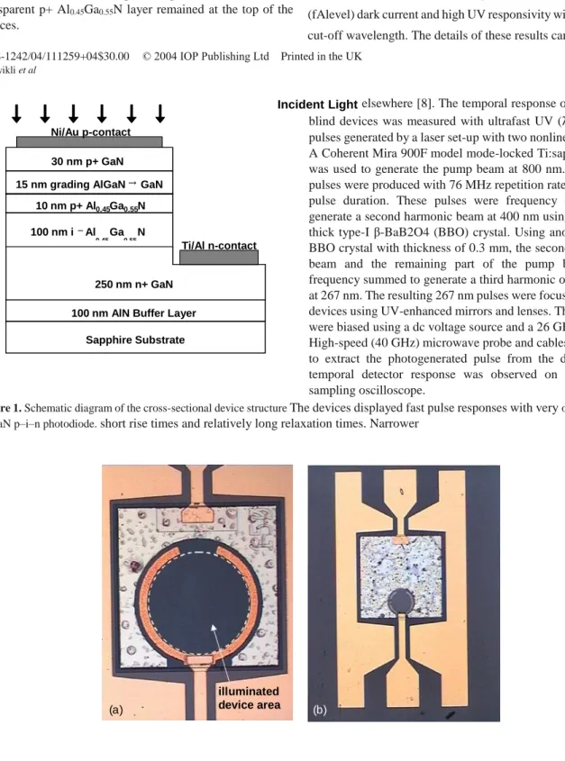
microwave compatible fabrication process. Figure 1 shows the cross-sectional device structure of the AlGaN p–i– n photodiode. Ohmic contacts were formed by annealed Ni/Au and Ti/Al alloys for p+ and n+ contacts, respectively. CCl2F2based reactive ion etching (RIE) process was utilized
for n+ ohmic and mesa isolation etch steps. The p–i–n detectors were passivatedwitha∼120nmthickSi3N4
layer,grownbyplasmaenhanced-chemical-vapour-deposition (PECVD). To make contact to the devices, thick (∼0.6 µm) interconnect metal pads were deposited in the final step of fabrication process. Microphotographs of completed AlGaN p–i–n photodiode samples captured by optical microscope and scanning electron microscope (SEM) are shown in figure 2.
On-wafer dc and microwave measurements of the fabricated devices were carried out. To observe the effect of absorbing p+ GaN cap layer on device performance, measurements were applied before and after recess etch. The p+ GaN cap layer and p+ grading layer were recess etched in three steps, each of ∼15 nm etch depth. The recess etch was done after the Si3N4 passivation layer was etched with
buffered HF etchant. The absorbing layers were etched using the same RIE recipe used for ohmic and mesa isolation etch
processes. After the 3-step etch process, 10 nm thick transparent p+ Al0.45Ga0.55N layer remained at the top of the
devices.
The AlGaN detector samples exhibited very low (fAlevel) dark current and high UV responsivity with ∼283 nm cut-off wavelength. The details of these results can be found
0268-1242/04/111259+04$30.00 © 2004 IOP Publishing Ltd Printed in the UK 1259
N Biyikli et al
Incident Light elsewhere [8]. The temporal response of the solar-blind devices was measured with ultrafast UV (λ∼ 267 nm) pulses generated by a laser set-up with two nonlinear crystals. A Coherent Mira 900F model mode-locked Ti:sapphire laser was used to generate the pump beam at 800 nm. The pump pulses were produced with 76 MHz repetition rate and 140 fs pulse duration. These pulses were frequency doubled to generate a second harmonic beam at 400 nm using a 0.5 mm thick type-I β-BaB2O4 (BBO) crystal. Using another type-I BBO crystal with thickness of 0.3 mm, the second harmonic beam and the remaining part of the pump beam were frequency summed to generate a third harmonic output beam at 267 nm. The resulting 267 nm pulses were focused onto the devices using UV-enhanced mirrors and lenses. The detectors were biased using a dc voltage source and a 26 GHz bias-tee. High-speed (40 GHz) microwave probe and cables were used to extract the photogenerated pulse from the device. The temporal detector response was observed on a 20 GHz sampling oscilloscope.
Figure 1. Schematic diagram of the cross-sectional device structure The devices displayed fast pulse responses with very of solar-blind
AlGaN p–i–n photodiode. short rise times and relatively long relaxation times. Narrower
ill d uminated evice area (a) (b) 30 nm p+ GaN nm n+ GaN 250
nm AlN Buffer Layer 100 Sapphire Substrate 100 nm i Al 0.45Ga0.55N 10 nm p+ Al0.45Ga0.55N GaN nm grading AlGaN 15 Ni/Au p-contact Ti/Al n-contact → −
Figure 2. Optical microscope photographs of completed solar-blind AlGaN p–i–n photodiodes with (a) 150 µm (dashed line surrounds the area of illumination) (b) 60 µm diameter. (c), (d) Scanning electron microscope photographs of a 30 µm diameter device.
1260
Time (ns)
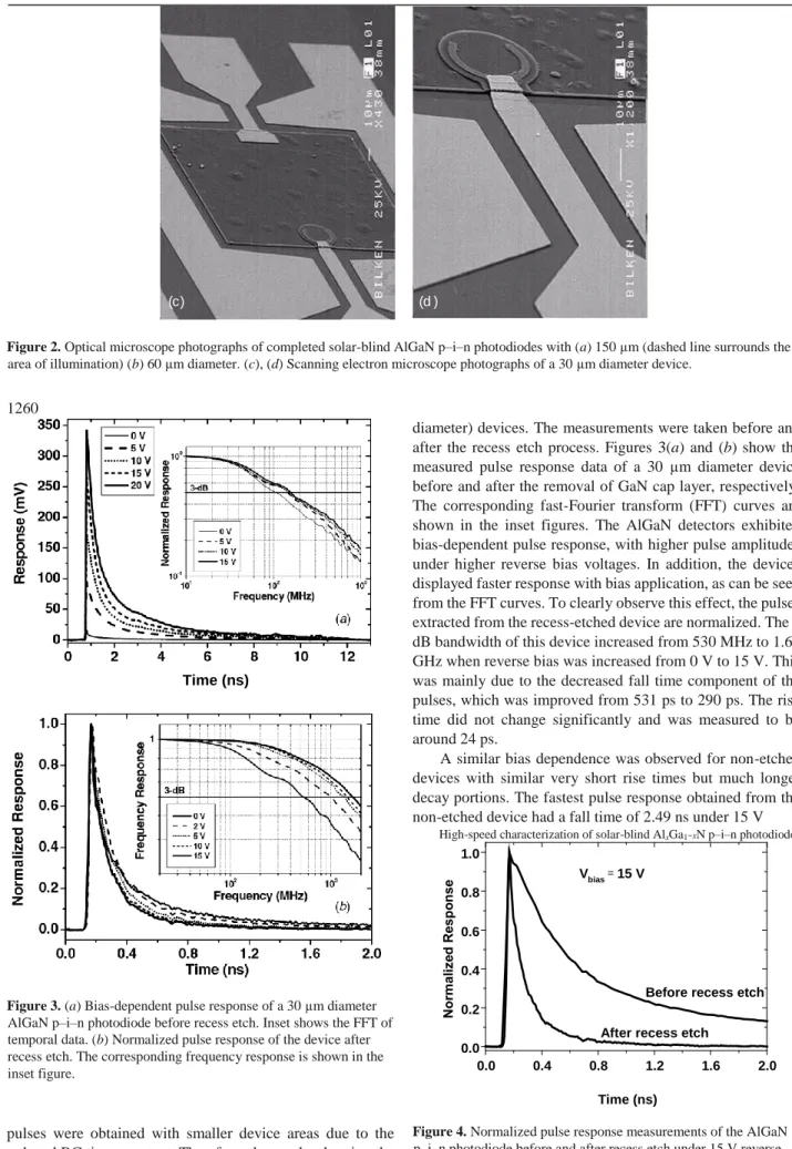
Figure 3. (a) Bias-dependent pulse response of a 30 µm diameter AlGaN p–i–n photodiode before recess etch. Inset shows the FFT of temporal data. (b) Normalized pulse response of the device after recess etch. The corresponding frequency response is shown in the inset figure.
pulses were obtained with smaller device areas due to the reduced RC time constant. Therefore, the results showing the fastest response were obtained with the smallest (30 µm
diameter) devices. The measurements were taken before and after the recess etch process. Figures 3(a) and (b) show the measured pulse response data of a 30 µm diameter device before and after the removal of GaN cap layer, respectively. The corresponding fast-Fourier transform (FFT) curves are shown in the inset figures. The AlGaN detectors exhibited bias-dependent pulse response, with higher pulse amplitudes under higher reverse bias voltages. In addition, the devices displayed faster response with bias application, as can be seen from the FFT curves. To clearly observe this effect, the pulses extracted from the recess-etched device are normalized. The 3 dB bandwidth of this device increased from 530 MHz to 1.65 GHz when reverse bias was increased from 0 V to 15 V. This was mainly due to the decreased fall time component of the pulses, which was improved from 531 ps to 290 ps. The rise time did not change significantly and was measured to be around 24 ps.
A similar bias dependence was observed for non-etched devices with similar very short rise times but much longer decay portions. The fastest pulse response obtained from the non-etched device had a fall time of 2.49 ns under 15 V
High-speed characterization of solar-blind AlxGa1−xN p–i–n photodiodes
Time (ns)
Figure 4. Normalized pulse response measurements of the AlGaN p–i–n photodiode before and after recess etch under 15 V reverse bias. (c) (d) 2.0 1.6 1.2 0.8 0.4 0.0 0.0 0.2 0.4 0.6 0.8 1.0 Vbias= 15 V
Before recess etch
reverse bias. The corresponding maximum 3 dB bandwidth was determined as 160 MHz. When compared, the recessetcheddeviceshowedastrongerbiasdependencethanthen onetched device with GaN cap layer. To make a fair comparison, it is useful to observe the normalized pulse responses for both devices. Therecess-etcheddevicedisplayedadecaytailwhich diminished rapidly under reverse bias, resulting in a significant increase in device bandwidth. This increase was attributed to the full depletion of the active layer and faster collection of drifting photo carriers. No carrier diffusion process existed in this device. For the non-etched device, a significant slow diffusion component was observed in the pulse response. Since this component originates from the carriers generated in the low-field p+ GaN layer, application of reverse bias cannot eliminate the slow decay. Hence, the device remains limited by carrier diffusion independent of applied bias voltage. The slight increase in 3 dB bandwidth corresponds to the faster collection of drifting carriers.
Figure 4 shows the normalized pulse response data measured before and after the recess etch under 15 V reverse bias. Pulse widths of 384 ps and 70 ps were measured before and after recess etching, respectively. A huge difference can be seen in the decay part of the pulse responses. The origin of the long decay tail observed in the non-etched device was the absorbing, low-field p+ GaN cap layer in which photogenerated electrons were moving by diffusion. Hence, the minority carrier diffusion mechanism was suggested as the bandwidth limitation of the non-etched p–i–n detector. The detector response became significantly faster after the removal of GaN cap layer. The 3 dB bandwidth performance was improved by an order of magnitude.
The exponential-like decay tail observed for the recessetched devices indicates an RC time constant limited response. However, when the decay tail was analysed, we were not able to fit the measurement data with a suitable first-order exponential decay. Instead, a good fit was realized with a second-order exponential decay function with two different time constants: 56 ps and 202 ps. While the fast one is rather closetothecalculatedRCtimeconstantofthedevice(∼38ps), the slower decay constant is much higher than this value. This shows that mechanisms other than RC time constant are limiting the device bandwidth performance. We suggest
1261 N Biyikli et al
that the second and longer time constant is mainly related to the trapping of carriers in Al0.45Ga0.55N active layer. While
moving towards the contact regions, photo-generated carriers can be trapped at the trap sites. The slower portion of the decay tail is possibly formed by the late arrival of such released carriers which were trapped in these sites.
To summarize the relaxation mechanisms, the response speedofthesolar-blindAlGaNp–i–nphotodiodebeforerecess etch was limited by the minority carrier diffusion of the photogenerated electrons in the low-field p+ GaN layer. With the removal of the absorbing p+ layers, we explained the faster response in that carrier diffusion component was eliminated and the pulse response became limited by the RC time constant and carrier trapping mechanism.
In conclusion, we have demonstrated solar-blind AlGaNbased p–i–n photodiodes with very fast pulse response. After the removal of p+ GaN cap layer, our devices exhibited 70 ps pulse widths along with 1.65 GHz 3 dB bandwidth performance.
Acknowledgments
This work was supported by NATO grant no. SfP971970, Turkish Department of Defense grant nos. KOBRA-002 and FUSAM-03.
1262 References
[1] Walker D, Zhang X, Kung P, Saxler A, Javapour S, Xu J and Razeghi M 1996 AlGaN ultraviolet photoconductors grown on sapphire Appl. Phys. Lett. 68 2100–01
[2] Lim B W, Chen Q C, Yang J Y and Asif Khan M 1996 High responsivity intrinsic photoconductors based on AlxGa1−xN Appl. Phys. Lett. 68 3761–2
[3] Monroy E 2003 III-Nitride-based UV photodetectors III-V Nitride Semiconductors Applications and Devices 1st edn vol 16 ed M O Manasreh (New York: Taylor & Francis) pp 525–91 [4] Parish G, Keller S, Kozodoy P, Ibbetson J P, Marchand H, Fini
P T, Fleischer S B, Denbaars S P, Mishra U K and Tarsa E J 1999 High-performance (Al,Ga)N-based solar-blind
ultraviolet p–i–n detectors on laterally epitaxially overgrown GaN Appl. Phys. Lett. 75 247–9
[5] Li T, Lambert D J H, Wong M M, Collins C J, Yang B, Beck A L, Chowdhury U, Dupuis R D and Campbell J C 2001 Low-noise back-illuminated AlxGa1−xN-based p–i–n
solar-lind ultraviolet photodetectors IEEE J. Quantum Electron. 37 538–45
[6] Biyikli N, Kimukin I, Kartaloglu T, Aytur O and Ozbay E 2003 High-speed solar-blind photodetectors with indium-tin-oxide
Schottky contacts Appl. Phys. Lett. 82 2344–6
[7] Biyikli N, Kimukin I, Kartaloglu T, Aytur O and Ozbay E 2003 High-speed solar-blind AlGaN-based
metal-semiconductormetal photodetectors Phys. Stat. Solidi(C) 0 2314–7
[8] Biyikli N, Kimukin I, Aytur O and Ozbay E 2004 Solar-blind AlGaN-based p–i–n photodiodes with low dark current and high detectivity IEEE Photon. Technol. Lett. 16 1718–20