Abstract
In the present study, firstly, a 4,4′-(9,9-dioctyl-9H-fluorene-2,7-diyl)bis(N,N-diphenylaniline) (FC) organic compound was synthesized and its structural and optical characterization were carried. Then, the effect on the device of the FC thin film prepared between n-type silicon substrate and gold metal by the spin coating technique was reported. The ideality factor (n), barrier height ( ΦB ) and series resistance ( Rs ) values of the prepared structure from the I-V data have been found at 1.08,
0.78 eV and 240 Ω at room temperature (300 K), respectively. According to the Gaussian distribution of the barrier height obtained from the various temperature ranges (220–380 K), the Φb0 and A* values from the ordinate intercept and the slope
of the modified Richardson curve of ln (I0∕T
2) − (q2
𝜎2
s∕2k 2
T2)
versus 1/T plot which has been found to be 0.97 eV and 114 A/cm2K2, respectively. Results indicate that the high barrier height is achieved for the Au/FC/n-Si metal–organic
layer-semiconductor diode as compared to the Au/n-Si metal–layer-semiconductor (MS) diode.
1 Introduction
The metal–semiconductor contacts formed by combin-ing two or more different materials are the basis of many semiconductor devices such as light emitting diodes, field effect transistors, solar cells, photodetectors, photodiodes and integrated circuits elements, and the interfacial layer
between the contacts is very important for device appli-cations because it affects the electrical properties of the devices [1–5]. In particular, the organic interface layer have a strong influence on the reliability and performance of a Schottky diode. Therefore, it is significant to define the organic interface properties of the diode because of its very high switching speed and a low forward voltage drop and to know the effect on the diode parameters such as the ideality factor, the barrier height and interface state density. For this reason, many studies are still being carried out today [5–10] and new organic materials are synthesized. Among these organic materials, the organic semiconductor compounds in the structure of fluorine-triphenylamine, which used as inter-facial layer, have a positive effect on device performance. Fluorene groups and triphenylamine groups have p-conju-gated system and they have wide triplet energy gaps [11,
12]. So, fluorene derivatives and triphenylamine groups are often used in organic materials. Especially, fluorene and its derivatives are preferred due to their luminescence, charge carrier transport and charge carrier mobility [13]. Fluorene moiety has been studied at aromatic 2,7 and also investigated at C9 position which is connected sp3 hybridized carbon atom [11, 12]. However, triphenylamine (TPA) has been employed as a building block to build numerous organic electro-luminescent materials [14, 15] because of its good hole transporting capability and prominent light-to-electrical
* Ö. F. Yüksel [email protected]
1 Department of Biotechnology, Faculty of Science, Selçuk University, Campus, Konya 42075, Turkey
2 Department of Chemical Engineering, Faculty of Natural Sciences, Architecture and Engineering, Bursa Technical University, Bursa 16190, Turkey
3 Department of Physics, Faculty of Science, Selçuk University Campus, Konya 42075, Turkey
4 Advanced Technology Research and Application Center, Selçuk University Campus, Konya 42075, Turkey 5 Gebze Technical University, Institutes of Energy
Technologies, Gebze 41400, Turkey
6 Department of Engineering Sciences, Faculty of Engineering, İzmir Katip Çelebi University, İzmir 35620, Turkey
7 Department of Energy Systems Engineering, Faculty of Engineering, Giresun University, Giresun 28200, Turkey
energy conversion efficiencies. Furthermore, polymers and oligomers of triphenylamine (TPA) have been widely studied as hole-transporting materials for a number of applications, such as light emitting diodes, organic field-effect transis-tors, perovskite solar cells, and photo refractive systems etc. [16–20]. So, in this study triphenylamine groups connected to C9 position provide higher hole transport, electron donor and good thermal stability to backbone.
In this study, we introduce organic compound based on the 4,4′-(9,9-dioctyl-9H-fluorene-2,7-diyl)bis(N,N-diphe-nylaniline) (FC) molecule and explore its application in relation to the fabrication of Schottky diode. Herein, the synthesis of triphenylamine material substituted with strong electron donor groups has been carried out and its optical property has been examined. Also, the effect of the use of FC organic film on the modification of electrical properties of Schottky diode has been investigated at a wide tempera-ture range, which is the main aim of this our study. For this aim, an n-type P-doped Si semiconductor wafer was used as the semiconductor substrate and FC organic semiconductor was formed on the n-Si wafer by means of a spin coating method. Then, a Schottky diode was prepared on this struc-ture. The current–voltage (I–V) characteristics of prepared Schottky diode were measured at the temperature range of 220 to 380 K and analyzed in frame of thermionic emission theory in detail. So, this research will reinforce further the currently prevailing interests on FC for possible optoelec-tronic applications.
2 Experimental techniques
2.1 Materials
All chemicals, potassium carbonate, and 4-(diphenylamino) benzeneboronic acid pinacol ester were purchased from Sigma-Aldrich and Abcr. 1,1′-Bis(diphenyl phosphino)-ferrocene] palladium (II) dichloromethane were purchased from TCI. Dichloromethane, toluene, 1,2-dimetoxyetane were purchased from Merck. All chemicals were used directly.
2.2 Synthetic route and characterization of FC
The synthetic route to FC is depicted in Fig. 1. 9,9-dido-decyl-2,7-dibromo fluorene (1.4 mmol, 700 mg) and 4-(diphenylamino)phenyl boronic acid pinacol ester (3.3 mmol, 1240 mg) have been dissolved in 1,2-dimeth-oxyethane (18 mL) in Schlenk. The system has been then quenched with argon gas by the addition of Pd (dppf) Cl2 (0,14 mmol, 114 mg) and K2CO3 (1 M) (3 mL). The
temperature has been brought to 90 °C and stirring con-tinued for a day. At the final phase of the reaction, the organic phase has been extracted with CH2Cl2/H2O and
the organic phase was evaporated. The product has been purified by the column chromatography with 1/1:CH2Cl2/ Hexane. The characterization of FC was made by 1H NMR
and 13C NMR spectroscopic tecniques. NMR spectra have
been recorded at room temperature on Bruker 400 MHz in CDCl3 as solvent. As seen in Figs. 2 and 3, the spectral data were in agreement with the desired structures.
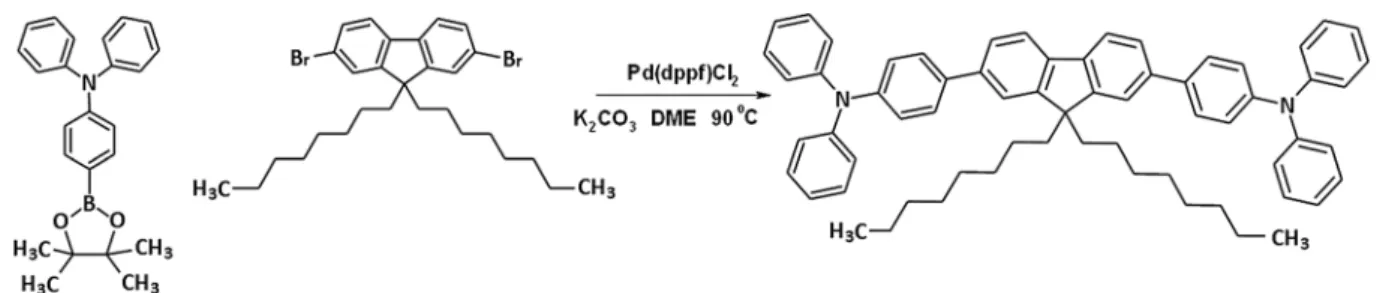
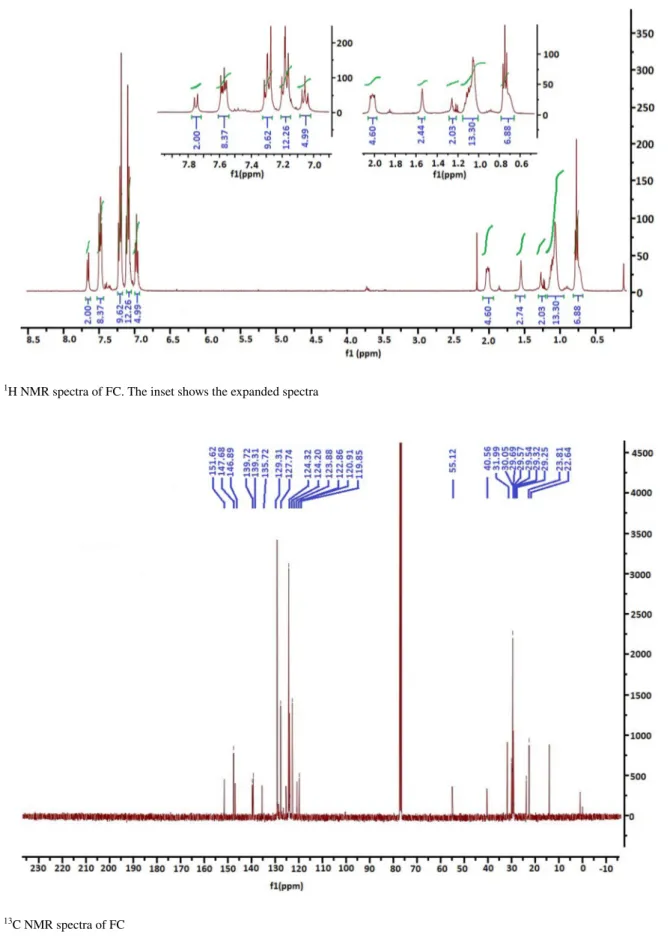
1H NMR (400 MHz CDCl 3): δ(ppm) 7.65 (d, 2H), 7.46 (m, 8H), 7.17 (m-10), 7.06 (m, 10H), 6.95 (m, 4H), 1.93 (m, 4H), 1.09 (m, 16H), 0.96 (m, 8H), 0.76 (m, 6H) (Fig. 2). 13C NMR (100 MHz CDCl 3): δ(ppm) 151.62, 147.68, 146.89, 139.72, 139.31, 135.72, 129.31, 127.74, 124.32, 124.20, 123.88, 122.86, 120.91, 119.85, 55.12, 40.56, 31.99, 30.05, 29.69, 29.57, 29.54, 29.32, 29.25, 23.81, 22.64 (Fig. 3).
We have prepared a solution from FC nanocrystals for the determination of the energy band gap. In this case, the Corning-1737 glass substrate has been cleaned in acetone, methanol and propanol for 5 min each by using an ultra-sonic cleaner and then dried in N2 gas. The glass substrate
has finally been cleaned by ultraviolet-generated ozone (UVO) cleaner. The FC has been dissolved in toluene-pro-panol with a concentration of 10 mg/ml. This solution was stirred for 30 min and the FC film has been prepared by spin coating technique at 1200 rpm spinning rate with the duration time of 60 s by using a Laurell Spin Coater in the MBraun glove box (nitrogen gas, 1.5–2.5 mbar pressure). The FC layer thickness was measured as 190 nm by stylus
Fig. 2 1H NMR spectra of FC. The inset shows the expanded spectra
profilometre Veeco Dektak 150. The surface properties of thin film were characterized by Zeiss Evo Ls 10 model Scanning Electron Microscope (SEM). The measurements of reflectance (R) and transmittance (T) of the film are performed at 300 K with normal incidence of light with integrating sphere between 200 and 2500 nm (2 nm step) with a double-beam spectrophotometer (JASCO model, V-670, UV–Vis–NIR, wavelength range: 190–2500 nm).
We have prepared Au/FC/n-Si/In device for the deter-mination of contact parameters. An n-type (P doped) Si wafer with 380 μm thickness, 20 Ω·cm resistivity, and (100) surface orientation is employed in this study. The wafer has been degreased with organic solvents to remove con-taminants and then cleaned using the Radio Corporation of America (RCA) cleaning procedure with the final dip in diluted HF for 60 s and then rinsed in 18 MΩ cm deion-ized water. Firstly, the ohmic contact has been prepared by evaporating the Indium (In) metal on the back side of the n-Si substrate with a thickness of 150 nm under vacuum of approximately 10−6 torr. Then, to provide a low resistivity
ohmic contact, a heat process has been made at 500 °C for 3 min in a vacuum. Secondly, Schottky rectifying contacts have been deposited using a metal shadow mask by evapo-rating gold (Au, 99.99%) metal in 10−6 torr vacuum on FC
organic film. The thickness and the active area of the recti-fying contacts are 150 nm and A = 3.14 × 10⁻⁶ m2,
respec-tively. Finally, we have fabricated Au/FC/n-Si/In device. The schematic representation of the device is shown in Fig. 4. The current–voltage characteristics of Au/FC/n-Si/In device have been measured using a Keithley 2410 SourceMeter at the temperatures range (220–380 K).
3 Results and discussion
3.1 Electrochemical properties
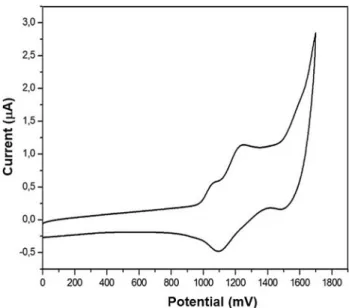
The electrochemical properties of FC and its highest occu-pied molecular orbital (HOMO)-lowest unoccuoccu-pied molec-ular orbital (LUMO) energy levels have been determined according to cyclic voltammetry method. The
measurement was performed in a 0.1 M solution of Bu4NPF6 in acetonitrile as a supporting electrode with a
scan rate of 100 mVs−1. A glassy-carbon was used as the
working electrode, platinum as the counter electrode and Ag/AgCl as the reference electrode. According to the vol-tammogram of FC scanned in the anodic potential region (Fig. 5). Due to two triphenylamine groups, which are con-nected with covalent bond to 2- and 7- carbon atoms of flu-orene center, two oxidation peaks are shown. The first and second oxidation processes were observed at potentials of 1.15 and 1.35 V, respectively and separated by 220 mV. The first oxidation peak was observed after the electrons of peripheral triphenylamine groups were oxidated simul-taneously. The second oxidation peak was observed after the electrons of fluorene center were removed. The starting point for first oxidation is 1.05 V. With the help of this value, the HOMO value of the molecule was measured as 5 . 4 4 e V u s i n g t h e f o r m u l a
EHOMO =[(Eonset
ox − E1∕2(ferrocene)) + 4.8] eV. (For the
meas-urement, the potential value of the redox couple in the ace-tonitrile solvent of ferrocene compound taken as reference is calculated 0.41 eV.) According to the absorption spec-trum of the molecule, its optical band gap is 3.01 eV, therefore, LUMO value is measured 2.43 eV using the formula Egopt= ELUMO− EHOMO.
3.2 Estimation of energy band gap
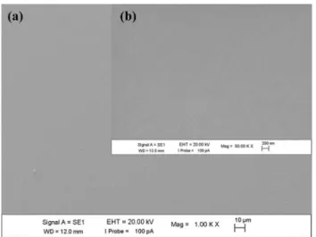
The SEM images having different magnification were obtained in Fig. 6. As seen in figure, it has been observed that the FC thin film was covered homogeneously and was non-porous.
Fig. 4 The schematic representation of the Au/FC/n-Si Schottky
The absorption coefficient (𝛼) of prepared organic film has been found by using both the reflectance and transmittance spectrum according to the following relation [21]
where d is the thickness of thin film, T is transmittance and
R is reflectance. To calculate the band gap energy of FC
organic film, we have examined the variation of 𝛼hv with ( hv − Eg)n , where Eg is the band gap, α is absorption
coef-ficient and hv is the photon energy. The certain knowledge of
Eg is significant for optoelectronic applications. The optical
band gap of the organic thin film is obtained by fundamental relation given by [22]
where B is a constant, the n changes on the nature of the transition. The n value is related to the density state distri-bution. It has 3, 2, 1/2 and 3/2 discrete values for indirect forbidden, indirect allowed, direct allowed transitions and direct forbidden, respectively. Figure 7 shows the plot of (𝛼h𝜈)2 against (h𝜈) of FC thin film. According to Fig. 7, the extrapolation of this plot for (𝛼h𝜈)2
= 0 gives the precise value of energy gap ( Eg ). The Eg value of the FC thin film
has been determined as 3.01 eV. Kaçus et al. [28] have deter-mined the energy band gap of the anthracene is 1.65 eV from optical measurements. They have also produced using anthracene Au/anthracene/n-Si Schottky diodes.
(1) 𝛼= 1 dln ( (1 − R)2 T ) (2) (𝛼h) = B(h − Eg )n
3.3 Determination of contact parameters of Au/ FC/n‑Si Schottky diode
Current–voltage (I–V) characteristics provide a beneficial knowledge about the diode parameters such as barrier height ( ΦB ), saturation current ( I0 ), ideality factor ( n ), series
resist-ance (Rs). The measured I–V characteristics of the diode
have been evaluated from the conventional Schottky barrier thermionic emission (TE) theory and is given by the rela-tions [2, 23].
where
is saturation current, T is the absolute temperature in Kelvin,
A is the contact area, q is the electronic charge, A∗ is the
effective Richardson constant and ΦB is the Schottky
bar-rier height. The n can be calculated from the slope of linear region of the forward bias ln(I) − V plot as
The ideality factor (n) has generally a value higher than unity. However,n equals to 1 for an ideal diode. High values of n can be attributed to the bias voltage dependence of the barrier height, barrier inhomogeneities, series resistance and presence of the interfacial layer [24].ΦB is the zero-bias
bar-rier height, which can be determined using the following equation (3) I= I0 [ exp( qV nkT ) − 1 ] (4) I0= AA∗T2exp ( −qΦB kT ) (5) n= q kT dV dln(I)
Fig. 6 SEM images of the FC thin film at different magnifications
The I–V plots of Au/FC/n-Si diode measured in both forward and reverse directions, between 220 and 380 K and from − 1 to 1 V, are shown in Fig. 8. According to Fig. 8, the all curves show diode like attitude and the value of current increases with increasing temperature. Ideal-ity factor can be used to define device and the material
(6) ΦB = kT q ln ( AA∗T2 I0 )
quality. If it can be build as an organic thin film between semiconductor and metal purposely. This interfacial film modifies the some characteristics of the devices. Because, barrier heights of semiconductor–metal structures can be manipulated by insertion of a dipole layer between the organic film and the semiconductor. The large values of ideality factor (n) may be referred to decrease the expo-nentially rise ratio in current due to space-charge injection into FC organic molecule at advanced voltage.
The temperature dependent-barrier height and ideality factor plot are illustrated in Fig. 9. The values of the bar-rier height and ideality factor of our diode have changed from 1.24 and 0.69 eV at 220 K to 1.03 and 0.82 eV at 380 K, respectively. We have observed that the value of ideality factor increases in the measured temperature range. Because of the increasing recombination/generation currents in the depletion region and series resistance val-ues of the FC structure. When the temperature increases, gradually electrons have suitable energy to pass over the larger barrier. As a result, the prevailing barrier height will increase as the temperature and voltage increases [25–30]. For this reason, the current flow through the higher ideal-ity factor and a lower barrier height will be important in the current transport.
Özmen and Yağlıoğlu [25] reported the characteristics of Au/P3HT:PCBM/n-Si diodes from I–V measurements at room temperature. They have calculated the values of electrical parameter ideality factor ( n ), barrier height ( ΦB ),
series resistance ( RS ). These values are 3.09, 0.73 eV, and
642 Ω, respectively. Kavasoğlu et al. [26] have reported the ΦB and n values in the range of 0.90 eV and 3.20 (at
110 K)-1.36 eV and 2.25 (at 330 K) for the Al/MEH-PPV/n-Si structure, respectively. Zeyada et al. [27] have reported the temperature-dependent I–V characteristics of Au/methyl vio-let 2B (MV2B)/n-Si diodes. They have found 2.67–0.67 eV for 300 K and 2.53–0.77 eV for 368 K for n and ΦB value,
respectively. Kaçus et al. [28] have reported the temperature-dependent I–V characteristics of Au/anthracene/n-Si diodes. They have found 2.67–0.67 eV for 300 K and 2.53–0.77 eV for 368 K for n and ΦB value, respectively. Furthermore,
they have also reported the temperature-dependent I–V char-acteristics of Au/anthracene/n-Si diodes in the temperature range of 140–300 K [29]. The value of the ideality factor and barrier height is changed from 3.00 to 0.43 eV at 140 K to 1.88 and 0.85 eV at 300 K, respectively. Martinez et al. [30] have calculated the diode parameters by using the stand-ard thermionic model, and the n value of PEDOT:PSS/n-Si Schottky diode was 7.2 and the barrier height was 0.58 eV. The barrier height of Au/FC/n-Si device has been calculated as 0.78 eV at 300 K. 0.78 eV value is greater than the Au/n-Si diode obtained in 0.62 eV [31] and 0.73 eV [32] too. This shows that FC interlayer increases the Schottky barrier height because of the space charge region of the n-Si.
Fig. 8 Experimental current–voltage characteristics for Au/FC/n-Si structure at different temperatures
Fig. 9 The temperature dependent-barrier height and ideality factor curves
The barrier height against ideality factor plot for the Au/ FC/n-Si device is given in Fig. 10. Ideality factors show a linear negative correlation with barrier height up to tem-perature. Tung et al. have reported [33, 34] that the ideality factor of a Schottky diode may decrease while the process temperature is increased if the Schottky diode has a distribu-tion of low Schottky barrier heights. Furthermore, Schmits-droff et al. [35] have reported that there is a relationship between the ideality factor and barrier height values of a Schottky diode. For Au/FC/n-Si diode, the homogeneous barrier height determined from the linear fit of the barrier height versus ideality factor which is 0.84 eV.
The Richardson constant ( A∗ ) value relates to the
effec-tive mass ( m∗ ) which is shown by A∗ =(4𝜋qk2h−3)m∗ . The
effective barrier height may be calculated from the Richard-son curve depending on saturation current ( I0 ). Equation (4)
can be converted to the following equation
Namely, from Richardson’s equation in Eq. (7), the exper-imental barrier height and the Richardson constant values can be evaluated. The experimental ln(I
0
T2) versus 1∕kT
curve should be corresponded to a straight line such that anintercept at ordinate of the experimental Richardson con-stant ( A∗ ) and slope giving the zero-barrier height
b0 . This
plot is shown in Fig. 11.
However, the Richardson plot showed linearity temperature with the linear portion corresponding to the activation energy ( Ea ) of 0.52 eV and a Richardson constant A* = 7.75 × 10⁻³
A/cm2K2 are determined. This value shows that the current
transport of the diodes deviates from TE theory and it can be (7) ln( I0 T2 ) = ln (AA∗) −qb0 kT
referred to the existence of FC between Au and n-Si and the barrier height inhomogeneity [2, 23, 33–35]. Taşçıoğlu et al. [36] have reported the forward bias I-V characteristics of Au/ PVA:Zn/n-Si diode between 80 and 400 K. The Ea and A∗
val-ues were calculated by researchers as 0.52 eV and 2.4 × 10⁻³
A/cm2K2 between 200 and 400 K, respectively. A∗ values
cal-culated by us, Taşcıoğlu et al. [36] and Gümüş et al. [37] are much lower than the common theoretical value of 112 A/cm2
K2 for n-Si [1, 2]. The deviation of the Richardson curves may
be result of the interfacial layer profile, potential fluctuations and the inhomogeneous barrier heights [38, 39].
The Schottky barrier height inhomogeneity of the Au/FC/n-Si Schottky diode has been introduced by the Gaussian distri-bution of the barrier heights [40–43]. The variation in the ide-ality factor values with barrier height values, their temperature dependence shows a non-ideal heterojunction behavior, which may be referred to the spatial barrier height distribution. The Gaussian distribution of the barrier heights gives the following well-known formula for the barrier height [44, 45].
where Φap is the apparent barrier height and 𝜎s is the
stand-ard deviation. Equation (8) shows that Φap versus 1/2kT plot
should be a straight line, from the intercept and slope of which one can calculate mean barrier height and the stand-ard deviation of the distribution. The experimental Φap
ver-sus 1/2kT curve is drawn by means of experimental data determined from Fig. 12. The values of Φb0 and 𝜎s are found
to be 0.99 eV and 0.11 mV, respectively. The Φap and 𝜎s
values were determined by Taşcıoglu et al. [36] as 1.06 eV and 0.11 V between 200 and 400 K, respectively. Gümüş (8) Φap= ̄Φb− q𝜎
2 s
2kT
Fig. 10 The ideality factor vs. the barrier height curve for the Au/
FC/n-Si device Fig. 11 The experimental ln(I0/T
2) versus 1/kT plots for the Au/FC/n-Si device
et al. [37] have reported that the forward bias I–V character-istics of Au/polypyrrole (PPy)/n-Si diode between 110 and 360 K. The Φap and 𝜎s values were determined by Gümüş
et al. [37] as 1.14 eV and 0.13 V between 110 and 360 K, respectively. Moraki et al. [46] have reported that the tem-perature dependent forward bias I–V characteristics of Au/ C20H12/n-Si diode between 160 and 380 K. The Φap and 𝜎s
values were calculated by Moraki et al. [46] as 1.12 eV and 0.15 V between 160 and 380 K, respectively.
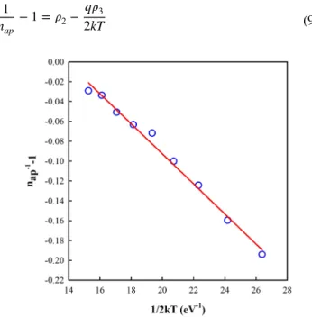
The observed variation of ideality factor with temperature gives the following well-known formula [44–47].
(9) 1 nap − 1 = 𝜌2− q𝜌3 2kT
where the coefficients 𝜌2 and 𝜌3 quantify the voltage
defor-mation of the barrier height distribution and nap is the
appar-ent ideality factor. Figure 13 shows the experimental versus 1/2kT curve drawn by means of experimental data. The fitted ideality factor nap curve shown in Fig. 13 is a straight line that gives voltage coefficients 𝜌2 = 0.205 V and 𝜌3 = 0.015 V
from the intercept and slope. The 𝜌2 and 𝜌3 values were
obtained by Taşcıoglu et al. [36] as 0.018 eV and 0.044 V between 200 and 400 K, respectively.
The Richardson plot presented at Fig. 11 according to Eq. (7) is now modified by combining Eqs. (8) and (9). According to the Gaussian distribution of the barrier height [42–46], we get,
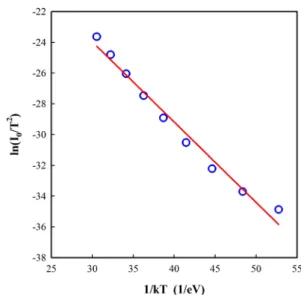
Figure 14 shows the modified ln (I0∕T2) − (q2𝜎s2∕2k 2T2) versus 1/T curve of Au/FC/n-Si diode. The Φb0 and A*
val-ues from the ordinate intercept and the slope of the modified Richardson curve of ln (I0/ T2) − (q2𝜎s2/ 2k
2T2)
. versus 1/T plot are determined to be 0.97 eV and 114 A/cm2K2,
respec-tively. Taşçıoğlu et al. [36], Gümüş et al. [37] and Moraki et al. [46] have reported that the Richardson constant with values of 121, 113.03 and 113.44 A/cm2 K2 found in the
temperature range 200–400 K, 110–360 K and 160–380 K, respectively. These values calculated by us, Taşcıoğlu et al. [36] and Gümüş et al. [37] are almost equal to the common theoretical value of 112 A/cm2 K2 for n-Si [1, 2].
Norde [48] has reported a method to determine the series resistance value. The modified Norde function can be rewrit-ten as follows (10) ln( I0 T2 ) − ( q2𝜎2 s 2k2T2 ) = ln (AA∗) −q ̄Φb kT
Fig. 12 Zero-bias apparent barrier height versus 1/(2kT) curves of Au/FC/n-Si structure according to Gaussian distributions
Fig. 13 Zero-bias ideality factor versus 1/(2kT) curves Au/FC/n-Si
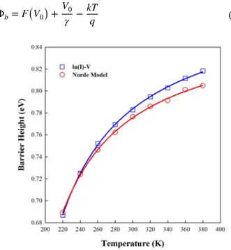
dis-where I(V) is the current found from the current–volt-age plot. γ is the first integer higher than n value. Figure 15
depicts F(V) versus V curves of Au/FC/n-Si diode in the temperature range 220–380 K. The temperature-dependent barrier height values of Au/FC/n-Si diode can be evaluated by using the equation
(11) F(V) = V 𝛾 − kT q ln ( I(V) AA∗T2 ) (12) Φb = F(V0) + V0 𝛾 −kT q
Figure 17 depicts the temperature dependency of series resistance (Rs) values determined from Norde methods for
Au/FC/n-Si diode. As shown in Fig. 17, the values of series resistance decrease with the increasing temperatures. These variations in the series resistance values verify the thermi-onic emission theory, describing the powerful dependency on the temperature. Deniz et al. [49] have reported that the forward bias I–V characteristics of Ni/Crystal Violet/n-Si diode between 200 and 340 K. The values of Φb and Rs are
found to be 0.57 eV and 11.833 kΩ for 200 K and 0.85 eV and 2.455 kΩ for 340 K according to Norde method, respec-tively. Aydoğan et al. [50] have investigated the effects of a thin Carmine organic layer in Au/n-Si diodes. They have determined that the values of Rs and Φb of the Au/
Carmine/n-Si diode have as 7.4 kΩ and 0.73 eV from Norde method at 300 K, respectively. Özaydın et al. [51] have fab-ricated the Au/Cu(II) complex/n-Si Schottky structure. The
qI
Fig. 15 Plot of F(V) versus V of the Au/FC/n-Si Schottky diode at various temperatures
Fig. 16 The barrier heights obtained from the conventional current– voltage relation and the modified Norde method as a function of
barrier height and series resistance of the structure obtained using Norde’s method were 0.77 eV and 6.7 kΩ, respec-tively. As mentioned above, the series resistance value calcu-lated by us for FC thin film shown in Fig. 17 is much lower than the series resistance values determined from Deniz et al. [49], Aydoğan et al. [50] and Özaydın et al. [51].
4 Conclusion
The 4,4′-(9,9-dioctyl-9H-fluorene-2,7-diyl)bis(N,N-diphe-nylaniline) (FC) organic thin film was deposited using spin coating method on n-type Si and glass substrate. To deter-mine the value of energy band gap of FC organic thin film, the optical absorption spectra of film was studied in the spectral range 200–700 nm. The indirect allowed transition of film was observed with the band gap of 3.01 eV. How-ever, the energy band gap value of FC organic compound was found as 3.01 eV by electrochemical method, and the Eg values found by using different methods are compatible
with each other. The electronic parameters of the Au/FC/n-Si diode have been introduced by I–V measurements in the temperature range from 220 to 380 K. I–V characteristics of Au/FC/n-Si diode have been introduced by using thermionic emission (TE) theory. The values of main electrical param-eters such as ideality factor, barrier height and saturation current determined from the forward bias LnI–V character-istic at 300 K have been found as 1.08, 0.78 eV, 12.46 × 10⁻⁸
A, respectively. Additionally, the values of series resistance have been calculated from the forward bias I–V data using the Norde method as 1200, 240 and 87 Ω for 220, 300 and 380 K, respectively. According to the Gaussian distribution of the barrier height, the Φb0 and A∗ values from the ordinate
intercept and the slope of the modified Richardson curve of ln(I0∕T2) − (q2𝜎2
s∕2k 2T2)
versus 1/T plot have been found to be 0.97 eV and 114 A/cm2K2, respectively.
We have reported that the FC organic thin film between Au and n-Si may be used to increase the barrier heights of the Au/n-Si contacts. The present results show that an FC interlayer is very dominant in improving the interfacial quality of the metal/organic layer/semiconductor devices. Furthermore, the optical absorption and device investiga-tions for FC thin film allow evidence for the applicability of FC organic film in the field of optoelectronic devices.
References
1. S.M. Sze, Physics of Semiconductor Devices (Willey, New York, 1981)
2. E.H. Rhoderick, R.H. Williams, Metal Semiconductor Contacts (Clarendon, Oxford, 1988)
3. S. Parasuraman, NOC: Fundamentals of electronic materials and devices (Course sponsored by Aricent), https ://nptel .ac.in/cours
es/11310 6065/Week%204/Lesso n9.pdf. Subject ID: 113106065, IIT Madras, 2017
4. A. Karabulut, A. Türüt, Ş. Karataş, J. Mol. Struct. 1157, 513–518 (2018)
5. A. Karabulut, İ. Orak, A. Türüt, Solid State Electron. 144, 39–48 (2018)
6. A. Djeghlouf, D. Hamri, A. Teffahi, A. Saidane, F.S. Al Mashary, M.M. Al Huwayz, M. Henini, I. Orak, A.M. Albadri, A.Y. Aly-amani, J. Alloys Compd. 775, 202–213 (2019)
7. A.V. Kesavan, A.D. Rao, P.C. Ramamurthy, Appl. Mater. Inter-faces 9, 28774–28784 (2017)
8. A. Kocyigit, I. Orak, Z. Çaldıran, A. Turut, J. Mater. Sci. 28, 17177–17184 (2017)
9. M.K. Rabinal, Appl. Surf. Sci. 382, 41–46 (2016)
10. S.H. Sung, N. Bajaj, J.F. Rhoads, G.T. Chiu, B.W. Boudouris, Org. Electron. 37, 148–154 (2016)
11. P. Shih, C. Chien, F. Wu, C. Shu, Adv. Funct. Mater. 17, 3514– 3520 (2007)
12. M. Irfan, K.D. Belfield, A. Saeed, RSC Adv. 5, 48760–48768 (2015)
13. Q. Yang, X. Jiang, Y. Xin, X. Zhao, J. Huang, S. Wang, R. Zheng, D. Mad, C. Wang, RSC Adv. 7, 54431–54440 (2017)
14. J. Kwon, M.K. Kim, J. Hong, W. Lee, S. Noh, C. Lee, S. Lee, J. Hong, Org. Electron. 11, 1288–1295 (2010)
15. H. Zhang, C. Liu, J. Xiu, J. Qiu, Dyes Pigments 136, 798–806 (2017)
16. M. Grigoras, T. Ivan, L. Vacareanu, A.M. Catargiu, R. Tigoianu, J. Lumin. 153, 5–11 (2014)
17. M. Thelakkat, J. Hagen, D. Haarer, H.W. Schmidt, Synth. Met. 102, 1125–1128 (1999)
18. S. Lv, Y. Song, J. Xiao, L. Zhu, J. Shi, H. Wei, Y. Xu, J. Dong, X. Xu, S. Wang, Y. Xiao, Y. Luo, D. Li, X. Li, Q. Meng, Electrochim. Acta 182, 733–741 (2015)
19. V. Mimaite, J.V. Grazulevicius, J. Ostrauskaite, V. Jankauskas, Dyes Pigments 95, 47–52 (2012)
20. T. Noda, I. Imae, N. Noma, Y. Shirota, Adv. Mater. 9, 239–241 (1997)
21. Ü. Akın, H. Şafak, V. Eskizeybek, A. Avcı, Ö.F. Yüksel, J. Nano-electron. OptoNano-electron. 9, 99–106 (2014)
22. F.A. Mir, S. Rehman, K. Asokan, S.H. Khan, G.M. Bhat, J. Mater. Sci. 25, 1258–1263 (2014)
23. S.M. Sze, K.K. Ng, Physics of Semiconductor Devices (John Wiley, Hoboken, 2007)
24. Ş. Aydoğan, Ü. İncekara, A.R. Deniz, A. Türüt, Solid State Com-mun. 150, 1592–1596 (2010)
25. Ö.T. Özmen, E. Yağlıoğlu, Mat. Sci. Semicon. Proc. 26, 448–454 (2014)
26. A.S. Kavasoğlu, F. Yakuphanoğlu, N. Kavasoğlu, O. Pakma, Ö. Birgi, S. Oktik, J. Alloys Compd. 492, 421–426 (2010)
27. H.M. Zeyada, A.A. Habashi, M.M. Makhlouf, A.S. Behairy, M.A. Nasher, Microelectron. Eng. 163, 134–139 (2016)
28. H. Kaçus, Ş. Aydoğan, D. Ekinci, S.V. Kurudirek, A. Türüt, Phys-ica E 74, 505–509 (2015)
29. H. Kaçus, A.R. Deniz, Z. Çaldıran, Ş. Aydoğan, A. Yesildağ, D. Ekinci, Mater. Chem. Phys. 143, 545–551 (2014)
30. O. Martinez, A.G. Bravo, N.J. Pinto, Macromolecules 42, 7924– 7929 (2009)
31. U. Aydemir, İ. Taşçıoğlu, Ş. Altındal, İ. Uslu, Mater. Sci. Semi-con. Proc. 16, 1865–1872 (2013)
32. E. Uğurel, Ş. Aydoğan, K. Şerifoğlu, A. Türüt, Microelectron. Eng. 85, 2299–2303 (2008)
33. R.T. Tung, Phys Rev B 45, 13509–13523 (1992)
34. R.T. Tung, J.P. Sullivan, F. Schrey, Mat. Sci. Eng. B 14, 266–280 (1992)
35. R.F. Schmitsdorf, T.U. Kampenand, W. Mönch, J. Vac. Sci. Tech-nol., B 15, 1221–1226 (1997)